High performance AlScN thin film based surface
acoustic wave devices with large electromechanical
coupling coefficient
Wenbo Wang1, P.M. Mayrhofer2, Xingli He1, Manuel Gillinger2, Zhi Ye1*, Xiaozhi Wang, Achim Bittner2, Ulrich Schmid2 and J.K.Luo3,1*
1. Dept. of Info. Sci. & Electr. Eng., Zhejiang University and Cyrus Tang Century for Sensor
Materials and Applications, 38 Zheda Road, Hangzhou 310027, China.
2. Inst. of Sensor and Actuator Systems, Vienna University of Technology, Floragasse, 7/2/
366-MST, A-1040, Vienna, Austria
3. Inst. of Renew. Energ. & Environ. Technol., University of Bolton, Deane Road, Bolton, BL3 5AB,
United Kingdom
Abstract: AlN and AlScN thin films with 27% scandium (Sc) concentration were synthesized by DC
sputtering deposition and used to fabricate surface acoustic wave (SAW) devices. Compared with
AlN based devices, the AlScN SAW devices exhibit much better transmission properties. Scandium
doping resulted in electromechanical coupling coefficient, K2, in the range of 2.0-2.2% for a wide
range normalized thickness, more than 300% increase compared with those of AlN-based SAW
devices, demonstrating the potential applications of AlScN in high frequency resonators and high
efficiency energy harvesting devices. The coupling coefficients of the present AlScN SAW devices
are much higher than that of theoretical calculation with some assumptions for AlScN piezoelectric
material properties, implying there is a need for thorough investigation on AlScN material properties.
Surface acoustic wave (SAW) device is one of the building blocks of modern electronics and has many applications such as frequency regulators, filters and duplexers,1 as well as sensors2 and microfluidics.3 SAW devices are normally made on bulk piezoelectric materials like LiNbO3.4 Recently, thin film based SAW devices have attracted more and more
attentions owing to their suitability for the integration with other devices on the same substrate. AlN is one of the most important thin film materials for the fabrication of such SAW resonators with high operation frequency due to its high acoustic velocity and stability at high temperatures.5 However AlN for SAW application is inherently limited by its low electromechanical coupling coefficient (K2) in the range of normally less than 1%,6 which is particularly critical for SAW-based actuator applications such as SAW microfluidics.7
Akiyama et al recently revealed that 43% scandium, Sc, doping in AlN can result in more than 400% increase in piezoelectric moduli d33.8Tasnádi et al performed theoretical analysis and confirmed a significant improvement in piezoelectric properties of AlScN.9 As K2 is proportional to d33,1 and the increase of d33 is accompanied only by a weak increase of the dielectric constants,10 thus scandium doping offers an approach to enhance the piezoelectric properties of AlN for the applications in acoustic resonators and energy harvesting etc.11,12 AlScN thin film with 46% Sc concentration has been used to fabricate SAW devices on SiC substrate, and demonstrated a significantly improved K2 value up to 3.8-4.5%.13 But this is for the Sezawa mode wave, rather than the fundamental mode of the SAW devices. Furthermore, the improvement in K2 is partially attributed to the high acoustic velocity in the SiC substrate. Since the piezoelectric properties of AlScN strongly depend on the concentration of Sc, and most material properties are still unknown which is even problematic for material modeling, AlScN remains to be mystic for device application. Therefore, there is a pressing need for more works on AlScN material and devices.
In this paper, thin film AlScN based SAW devices have been fabricated on low cost silicon substrate with 27% scandium concentration and exhibited excellent performance with high K2 values (>2%) for the fundamental mode, which is much higher than that of the theoretical analysis, demonstrating the great potential applications.
sputtering from a 100 mm AlScN alloy target (purity 3N) at a process pressure of 2.5 μbar, a plasma power of 400 W and a target-substrate distance of 65 mm. 25% Argon was added to nitrogen gas as the process gas since it was previously observed that the admixture of argon is a crucial tool in obtaining c-axis oriented AlScN for lower concentration of Scandium.15The AlN thin films were deposited by DC reactive sputtering from a 150 mm Al target (purity 5N) with pure nitrogen as process gas, 2 μbar pressure, a plasma power of 800 W and a target-substrate distance of 65 mm. Both types of thin films with the same thickness of ~2 μm were deposited on unheated substrates. After deposition, rapid thermal annealing (RTA)(RTP CT-100M, Premtek) was carried out to these films at 800 °C for 10 min. The heating rate was set to 10 °C/sec and cooling down naturally under pure nitrogen flow rate of 1 l/min.
SAW devices based on both AlN and AlScN (with 27% Sc) thin films were fabricated for comparison. The interdigitated transducers (IDTs) were made by conventional photolithography and lift-off process using Ti/Au. The metal layers of 5 nm Ti and 60 nm Au were deposited by E-beam evaporation sequentially. The IDTs have 50 pairs of fingers and the wavelength, λ, of SAW devices is varied from 16 μm to 24 μm. The delay line of SAW devices is 20λ. These SAW devices were characterized by an Agilent E5071C network analyzer.
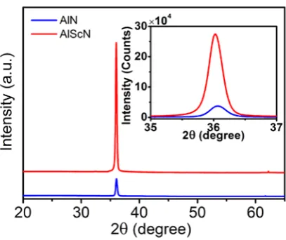
X-ray diffraction (XRD) was used to analyze the crystal structure of the deposited thin films with the same condition as in the previous work.16 Fig. 1 shows the XRD curves for both the AlN and AlScN thin films that exhibit strong peaks at 36.06° and 36.05°, respectively, corresponding to (0002) crystal orientation of the wurtzite structure. The XRD intensity of the AlN (0002) peak increases significantly for the AlScN film, consistent with the results reported by Akiyama et al, indicating that the thin film has a highly pronounced c -axis orientation.8 The full width at half maximum (FWHM) of the diffraction peak for AlN and AlScN is 0.25° and 0.36°, respectively, showing both the thin films have excellent crystalline properties.
FIG. 1. XRD patterns for AlN and AlScN thin films on (100) Si with 800°C post-deposition annealing.
FIG. 2. Transmission and reflection spectrum of AlScN based SAW device. The thickness of AlScN film is ~2 μm and the wavelength of SAW device is 16 μm.
substrate are even better than AlN/sapphire-based SAWs,19 though sapphire substrate possesses much larger hardness, hence higher acoustic velocity, than those of Si, further demonstrating the usefulness of scandium doping in AlN for SAW applications.
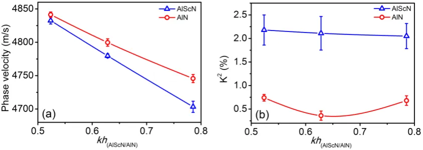
For thin film structure SAW devices, the phase velocity (vp) of acoustic wave is determined by both the material properties of the layers and their interfaces. The phase velocity of the Rayleigh mode wave can be calculated using the basic equation of vp = λf0, where f0 is the resonant frequency. The phase velocities of AlScN and AlN based devices are shown in Fig. 4(a), and the acoustic velocity of the AlScN SAW devices is smaller than that of the AlN device. This is believed to be mainly caused by the softening of the crystal structure with the introduction of scandium.20 With scandium doping, a competition of Al3+ and Sc3+ to the coordination with nitrogen is introduced, that weakens the resistance of nitrogen displacement in crystal structure, and increases the unit cell volume.9,20-22 These lead to an increase in piezoelectric constant e33, while on the other side they also reduce the
stiffness constant, c33.21 Therefore, the elastic softening contributes to the lower acoustic velocity of the AlScN-based devices.
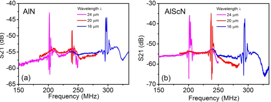
FIG. 3. Comparison of transmission spectrum of AlN (a) and AlScN (b) based SAW devices, the
thickness of both the thin films is ~2 μm, and the wavelength of both types of devices is varied from 16 μm to 24 μm.
substrate, i.e. much higher acoustic velocity in these substrates than in Si (~4680 m/s) we used. Also it is noticeable that although AlScN possesses a high acoustic velocity, the measured phase velocity for both types of the devices is not very high, but close to the acoustic velocity in Si. This is mainly due to the “very thin” piezoelectric film as compared to the wavelength, which makes acoustic waves mainly propagate in the Si substrate, rather than in the AlN and AlScN layer.
FIG. 4. Phase velocity (a) and coupling coefficient (b) of AlScN and AlN based SAW devices as a
function of normalized thickness of thin films.
The coupling coefficient is a very important parameter for piezoelectric device applications.23,24 As discussed above, scandium doping to AlN can enlarge the unit cell volume, leading to an increase of e33, but a decrease of c33.9,20,22 Since the piezoelectric moduli is approximately d33=e33/c33, Sc doping to AlN increases d33 significantly, hence K2 in turn. Let’s estimate the K2 value for our devices, which can be calculated from the measured data of the reflection spectrum with the following equation17,25
𝐾2 = π 4𝑁
𝐺(𝑓0)
𝐵(𝑓0) (1)
smaller than 4.5% obtained from the AlScN/6H-SiC-based devices, the latter has 46% scandium concentration at larger normalized thickness (hk~3.0-4.0), and most importantly it is for the Sezawa mode wave which is normally much larger than the Rayleigh mode.26 Furthermore, both the larger normalized piezoelectric layer and SiC substrate which possesses large shear bulk velocity, can confine more acoustic energy in the AlScN layer and contribute to larger K2 value.13 Our K2 values are even better than the result of K2<1% at a similar normalized thickness (h/λ~0.1) for the AlScN (40% Sc) Lamb wave resonators reported by Konno et al,12 indicating excellent performance of our devices. It is worth pointing out that theoretical calculation based on some assumptions for material properties shows much smaller K2 values (<<1% for hk=0.5-4.0, Figs. 1 and 2) for the fundamental mode13 and the Lamb wave12 than what we have obtained, implying the assumptions for material properties and the model for theoretical analysis may not be right, and may need to be reconsidered carefully. There may exist a scandium concentration region for the AlScN materials with better coupling coefficient and piezoelectric properties.
In summary, we have deposited AlScN thin film with 27% scandium doping on Si substrate and fabricated SAW devices thereof. The Rayleigh mode resonance has been observed with excellent transmission properties. Electromechanical coupling coefficients of the AlScN based devices are more than 2% for a wide range of normalized thickness, more than 300% increase compared to those of the AlN-based devices, indicating that scandium doping can significantly improve the piezoelectric properties of AlScN, and its thin film is a promising candidate for device applications.
Acknowledgement: The authors would like to acknowledge NSFC (No. 61274037), Fundamental Research Funds for the Central Universities of China (2014QNA5003), Austrian Science Fund (FWF, P25212-N30) and EU COST program (IC-1208) for the financial support for this project. The authors also would like to acknowledge the financial support by the Innovation Platform of Micro/Nanodevices and Integration System, Zhejiang University.
Reference
1
J. T. Luo, F. Pan, P. Fan, F. Zeng, D. P. Zhang, Z. H. Zheng, and G. X. Liang, Appl. Phys. Lett. 101
2
V. Chivukula, D. Ciplys, M. Shur, and P. Dutta, Appl. Phys. Lett. 96 (23), 233512 (2010). 3
Leslie Y. Yeo and James R. Friend, Ann. Rev. Fluid Mech. 46 (1), 379 (2014). 4
C. D. Wood, S. D. Evans, J. E. Cunningham, R. O’Rorke, C. Wälti, and A. G. Davies, Appl. Phys. L ett. 92 (4), 044104 (2008).
5
C. Caliendo and P. Imperatori, Appl. Phys. Lett. 83 (8), 1641 (2003). 6
C. J. Zhou, Y. Yang, H. Jin, B. Feng, S. R. Dong, J. K. Luo, T. L. Ren, M. S. Chan, and C. Y. Yang, Thin Solid Films 548, 425 (2013).
7
J. Zhou, M. DeMiguel-Ramos, L. Garcia-Gancedo, E. Iborra, J. Olivares, H. Jin, J. K. Luo, A. S. Elh ady, S. R. Dong, D. M. Wang, and Y. Q. Fu, Sens. Actuators B 202, 984 (2014).
8
M. Akiyama, T. Kamohara, K. Kano, A. Teshigahara, Y. Takeuchi, and N. Kawahara, Adv. Mater.
21 (5), 593 (2009). 9
F. Tasnádi, B. Alling, C. Höglund, G. Wingqvist, J. Birch, L. Hultman, and I. A. Abrikosov, Phys. Rev. Lett. 104 (13) (2010).
10
M. A. Moram and S. Zhang, J. Mater. Chem. A 2 (17), 6042 (2014). 11
S. Barth, H. Bartzsch, D. Gloess, P. Frach, T. Herzog, S. Walter, and H. Heuer, in Proc. IEEE Int. Ultrason. Symp. (IEEE, 2013), pp. 1351.
12
A. Konno, M. Sumisaka, A. Teshigahara, K. Kano, K. Hashimo, H. Hirano, M. Esashi, M. Kadota, and S. Tanaka, in Proc. IEEE Int. Ultrason. Symp. (IEEE, 2013), pp. 1378
13
K. Y. Hashimoto, S. Sato, A. Teshigahara, T. Nakamura, and K. Kano, IEEE Trans. Ultrason. Ferr oelectr. Freq. Control 60 (3), 637 (2013).
14
M. Schneider, A. Bittner, F. Patocka, M. Stöger-Pollach, E. Halwax, and U. Schmid, Appl. Phys. L ett. 101 (22), 221602 (2012).
15
P. M. Mayrhofer, C. Eisenmenger-Sittner, M. Stöger-Pollach, H. Euchner, A. Bittner, and U. Schmi d, J. Appl. Phys. 115 (19), 193505 (2014).
16
J. Zhou, X. L. He, H. Jin, W. B. Wang, B. Feng, S. R. Dong, D. M. Wang, G. Y. Zou, and J. K. Luo, J. Appl. Phys. 114 (4), 044502 (2013).
17
O. Elmazria, V. Mortet, M. El Hakiki, M. Nesladek, and P. Alnot, IEEE Trans. Ultrason. Ferroelect r. Freq. Control 50 (6), 710 (2003).
18
J. Zhou, H. F. Pang, L. Garcia-Gancedo, E. Iborra, M. Clement, M. De Miguel-Ramos, H. Jin, J. K. Luo, S. Smith, S. R. Dong, D. M. Wang, and Y. Q. Fu, Microfluid. Nanofluid. (2014).
19
T. Aubert, O. Elmazria, B. Assouar, L. Bouvot, and M. Oudich, Appl. Phys. Lett. 96 (20), 203503 (2010).
20
R. Matloub, M. Hadad, A. Mazzalai, N. Chidambaram, G. Moulard, C. S. Sandu, Th Metzger, and P. Muralt, Appl. Phys. Lett. 102 (15), 152903 (2013).
21
S. Zhang, W. Y. Fu, D. Holec, C. J. Humphreys, and M. A. Moram, J. Appl. Phys. 114 (24), 24351 6 (2013).
22
C. Tholander, I. Abrikosov, L. Hultman, and F. Tasnádi, Phys. Rev. B 87 (9) (2013). 23
Z. Yan and L. Y. Jiang, J. Phys. D Appl. Phys. 44 (7), 075404 (2011). 24
G. Bu, D. Ciplys, M. Shur, L. J. Schowalter, S. Schujman, and R. Gaska, Appl. Phys. Lett. 84 (23), 4611 (2004).
25
W.R. Smith, H.M. Gerard, J. H. Collins, T.M. Reeder, and H.J. Shaw, in IEEE T. Microw. Theory (1969), Vol. 17, pp. 856.
26