DYNAMIC COMPENSATION OF ELECTRICAL POWER SYSTEMS
USING MULTILEVEL VOLTAGE SOURCE INVERTER
S. H. Hosseini and M. T. Haque
Department of Electrical Engineering,University of Tabriz Tabriz, Iran, hosseini@tabriz.ac.ir - tarafdar@tabriz.ac.ir
R. M. Mathur
Department of Electrical and Computer Engineering,University of Western Ontario London, N6A 5B9, Canada
(Recived: March 8, 1998 - Accepted in Final Form: May 29, 2001)
A N ew Static Va r G enerator (SV G ), u sing cascaded full-bridge inverte rs (FBI) Abstract
with binary ou tput levels an d the par alle l connections of t wo ca sca de d inverter s by m eans of curren t sharing rea ct or in ea ch phas es is introduced. The ne w M -level inver ter , whe re M is 2n+2 - 3, consists of only 2n single-phase full bridges for each phases. The proposed technique not o nly in crea ses t he cu rren t capa cit y of p ropos ed SV G bu t also de cre a ses t he ou tpu t har monic cont ent s. A lso, it ca n be connect ed direct ly to t he dist ribut ion syste m wit hout a t ra nsfor m er. S im ulat ion re su lt s , bas e d o n t he P S CA D /E M T D C, a h igh per form a nce elect romagnetic tra nsient sim ula tion program, a re used t o illu strate t he fle xibility of cont rol action and also the performance of the proposed SVG in a power system environment.
Multi-Level VSI, Parallel Connection of VSIs, Harmonic Elimination, SVG KeyWords
° ºo®½BÇM pB–ñU¥Q ¨BªU ºBµoUn±®½A ¬joŸ ºow ðªñM »ñ¼UBTwA Var k½k] k§±« ð½ ³§Bš« -½A nj
²k¼ña
¬C nj³ÇŸ ³d†ÇwMk½kÇ] ¤kLÇ« /SwA ²kÇ{ ³ÇÄAnA pBÇ—-¼ÇM u¯AoU ðªñM ˜±— ºow ¤kL« °j ¬j±ª¯ ºpA±« ¬A±U»« B´®U ³¯ ºjB´®z¼Q ¤kL« 𪟠³M ° ²j±M pB—oµ nj pB–ñU ¥Q ¨BªU oUn±®½A2n¥«B{ k{BM»« M=2n+2-3 -¼ÄBQ »¦¼i ¤kL« »]°oi Z±« ¥ñ{ »ñ¼¯±«nBµ º±Td« ³ñ¦M joM ¿BM Ao¯C »]°oi rBT§° ° ¤kL« ¬B½o] S¼—o‹ -¼®`ªÇµ ° ¤kLÇ« ¤oT®ÇŸ ”B†íǯA S¼¦MBÇ› °PSCAD/EMTDC nAq—A ¨o¯ …w±U ºpBw³¼L{ [½BT¯ /j±M kµA±i /SwA ²k{ ²jAj ¬Bz¯ Rnk›·ñL{ ð½ ð¼«B®½j ¬±¼wAq¯BPªŸ ºAoM ¤kL« é½ow joñ¦ªîINTRODUCTION
Mo dern h igh -t ech in du stry n eeds reliable and high quality p ower sup ply. Un desirable su pp ly qu alit y can lead t o an in adeq u at e q u alit y o f pro du cts, in terrup t io n o f imp ort an t in dust rial precesses an d therefore to econ omic losses. In addit ion , offices an d co n su mer s expe ct h igh su pp ly qu alit y to safe gu ard th eir equ ip men t, which is sensitive to power quality. To minimize vo lt age fluct u at io n s an d imb alan ces, react ive po wer comp en sat io n is no w widely u sed . It is also used t o in cr ease t h e po wer t ran smissio n ca p aci t y o f a c l in e s. F a st an d o p t i mall y
SV Gs, b ase d on vo lt age so u rce in vert ers emp lo yin g gate-t urn -off (G TO) th yrist ors, ar e showing promise of improving power factor and stabilizin g t ran smissio n syst ems. An SVG can adjust the amplitude of the ac voltage, by means o f p u lse -wid t h mo d u la ti o n ( P WM ) o f th e in ver ter o r by con t ro llin g th e dc b us volt age, t h u s in ject in g e it h e r a le ad in g o r lagg in g reactive power. A pulse-width-modulated SVG, in which th e d c voltage is main tain ed co nstant, can respond rapidly to changing reactive power de man d a t t h e e xp e n se o f in cr e asin g t h e switching and snubbing losses. Due to the rating restriction of the inverter switching devices, it is difficult to apply SVGs, using two or three-level in ve rt e rs fo r h igh vo lta ge an d h igh p o wer ap p licat ion s. To o ver come t his d isad vant age, SVG systems u singmul til evel invertersh ave at tr acted tre men do u s in t erese t. T he gen eral structure of a multilevel inverter is to synthesize a sin u so id al vo l tage fo rm sever al leve ls o f vo lt ages, t yp ically o b t aine d fr o m cap acit or vo lt ag es so u rces. As t h e n u mb er o f leve ls in cr e ases, t h e syn t h e size d st ai rcase wa ve app r oaches t h e sin u so id al wave r esu lt in g in reduced harmonic distortion. The goal here is to minimize the harmonic distortion in the system, but at the same time the inverter scheme should be simple and compact. The different multilevel VSI sch emes st ud ied an d t ested so far in clud e dio d e-clamp , flyin g-capacit o r an d cascad ed separate dc source inverters [5,6].
T o ach ie ve a b et t er wave fo rm an d al so higher p ower rat ings, in th is pap er, full-brige inverter units with binary output levels and the parallel co nn ection s o f t wo cascaded inverters using a current sharing reactor in each phases is proposed. The new M-level inverter, where M is 2n+ 2-3, con sists o f o n ly 2n sin gle-p h ase fu ll
br idge s fo r each p h ase , e .g. wit h nÂ2, t h is invert er can gen erate almo st sin uso idal volt age waveform with the least component count while ret ainin g fun ctio nal modu larit y. Th e switch in g t imin g an g le s a re v ar ie d t o co n t r o l t h e fu n d a me n t a l o u t p u t vo lt ag e a n d al so t o
minimize waveform distortion, and are stored in the switching pattern table. This new multilevel inverter eliminates excessively large numb er of bu lk y tran sfo rmers re qu ired by co nven tio n al multi-pulse inverters. It is suitable for flexible ac tr ansmissio n syst ems ( F ACT S) ap p licat io n s in clu d in g st at ic var ge n erat io n , p owe r-lin e conditioning, series compensation, phase shifter, and voltage balancing because each dc capacitor v o l t a g e ca n b e se l f -m a i n t a i n e d a n d indep en dent ly con tro lled with ou t addition al dc sources.
To illu st rat e t h e cap abilit ies of p ro p o sed SVG fo r re act ive p o wer co mp en satio n , t h e detailed three phase transient simulation in 13.8 kV dist r ib u t io n syst em is car ried o u t u sin g PSCAD /E M TD C simu lat io n p ro gram [7] fo r d iffe re n t o p e ra t in g co n d it io n s. T h is n ew con vert er t o po logy can be easily ad ap t ed n ot only to reduce the dynamic distortion of power systems b ut also fo r ot her ap plicatio n s such as fu el cell an d p h o t o vo lt aic u tilit y int erface systems where the sources are originally isolated dc sources. Another possible application of this n ew co nvert er is fo r ad justab le sp eed d rive s req u ir ing h igh efficien cy, wh ich may n o t b e achievable with PWM techniques.
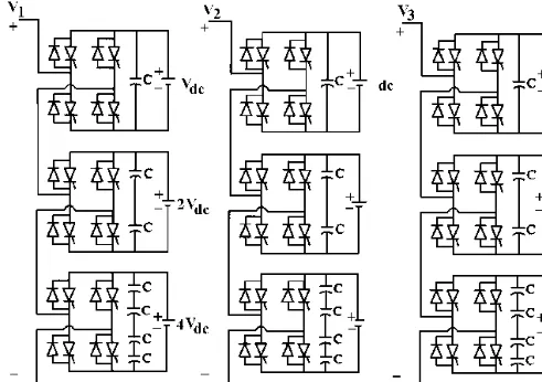
PROPOSED STATICSYNCHRONOUS COMPENSATOR
Figure 1.Proposed simple binary multilevel voltage.
between the ac system and a dc electric energy sou rce storage, in oth er wo rds with iso lated d c sources in dc side of FBIs it is possible to use it also as a unified power flow controller (UPFC).
A. Structure and Principle of Operation of
F i g u r e 1 s h o ws t h e
a Simple BMVSI
sin gle-p h ase co n figu rat io n o f t h e p ro p o sed BM VSI. I t co nsists o f 3 Fu ll-b rid ge in ver ter (FBI) units connected in cascade to generate a 23 + 1-1 = 1 5 st ep o u t p u t vo lt ag e o ver h alf
fu n d amen tal cycle. E ach FBI h as its o wn d c source i.e. Vdc, 2Vdc and 4Vdc this new BMVSI
do es n o t re qu ire any t ran sfo r mers, clampin g diodes, or flying capacitors and its advantage is that by using only 3 FBI units in each phases a 15-level ap p ro ximate ly sin u so idal an d fu lly
Fi gure 2.G ene rat ed wa veform s by single -pha se sour ce inverter (BMVSI) topology. BMVSI in its ac side.
co n tr o llab le ou t p u t vo ltage is ach ieve d [8 ]. Figure 2 sh o ws wavefo rms gener ated by each FBI and also the output voltage u1. It is the sum
of 3 inverter u nit o ut pu t volt ages, i.e.ub1,ub 2
and ub3:
(1)
u1 = ub1 + ub2 + ub3
Each FBI u nit generat es th ree-level ou tp ut , e.g. FBI- 1 generates+ Vdc, 0 and - Vdc which is
mad e p o ssib le b y co n n ectin g t h e d c-so u rce seq u en tially t o t h e ac side via th e switch in g devices s1, s2, s3 an d s4. The diod es an d G TO s
form a switching group which is bi-directional in current and uni-directional in voltage.
Table 1 lists 15 levels of the output voltages an d t h eir co rr esp o n d in g swit ch st at es fo r single-phase configuration of Figure 1 over one half fundamental cycle. State condition 0 means th at t h e swit ch is o ff an d 1 me an s t h at t h e swit ch is o n. As seen in th is T ab le th e t ot al number of switchings of FBI-1, FBI-2 and FBI-3 fo r e ach h al f cycl e is 4 , 2 an d o n l y 1 respectively. The waveform ofu1, illu strated in
TABLE 1. Fifteen Levels of the Output Voltage and Their Cor r es po n d i n g S wi tc h S tat e s for S i n gl e -ph as e Co nfi gu rati on of BMVS I Over an Half Fu nd amen tal Cycle.
Switch states
n1 =
s12 s11 s10 s9 s8 s7 s6 s5 s4 s3 s2 s1 0 1 0 1 0 1 0 1 0 1 0 1 7Vdc 0 1 0 1 0 1 0 1 0 0 1 1 6Vdc 0 1 0 1 0 0 1 1 0 1 0 1 5Vdc 0 1 0 1 0 0 1 1 0 0 1 1 4Vdc 0 0 1 1 0 1 0 1 0 1 0 1 3Vdc 0 0 1 1 0 1 0 1 0 0 1 1 2Vdc 0 0 1 1 0 0 1 1 0 1 0 1 Vdc 0 0 1 1 0 0 1 1 0 0 1 1 0 0 0 1 1 0 0 1 1 1 0 1 0 -Vdc 0 0 1 1 1 0 1 0 0 0 1 1 -2Vdc 0 0 1 1 1 0 1 0 1 0 1 0 -3Vdc 1 0 1 0 0 0 1 1 0 0 1 1 -4Vdc 1 0 1 0 0 0 1 1 1 0 1 0 -5Vdc 1 0 1 0 1 0 1 0 0 0 1 1 -6Vdc 1 0 1 0 1 0 1 0 1 0 1 0 -7Vdc (2)
u1 = k=1
È
S V2k - 1 Sin [(2k-1)wt]
where V2k-1is the amplitude of (2k-1)th output
harmonic (k = 1,2,3,...):
(3) V2k-1= _______
i=1 N
S Vdc cos [(2k-1)qi]
4 (2k-1)p
with N= 2n-1, in a 15-leve l BMVSI, n = 3 and
N = 7 . T h e swi t ch i n g t im in g a n g le s qi
(i=1,2,3,...,7) for this 15-level BMVSI, are to be calculat ed o ff -lin e to e limin ate so me lo wer ord er harmo n ics fo r a given mo du lation ind ex
(MI), which is defined as _____, where VV1 1is the
V1max
amplitude of the fundamental component of the BMVSI output phase voltage:
(4) V1= __
i=1 7
S Vdc cos (qi)
4
p
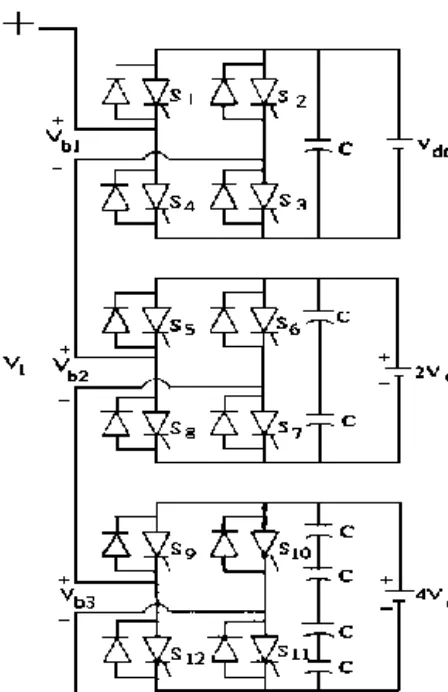
TABLE 2. Th e S witch in g Timin g An gle Con trol of BMVSI for Different Values of MI = V1/V1max.
Switching angles MI = q7 q6 q5 q4 q3 q2 q1 89.08 74.15 65.06 56.12 48.86 40.55 25.88 0.510 89.26 70.19 62.22 54.7 47.46 33.81 20.23 0.550 84.47 58.82 66.71 52.35 39.02 33.54 14.29 0.600 67.40 62.67 54.22 50.34 35.19 23.72 16.10 0.680 67.81 58.47 57.06 45.25 31.56 22.02 13.51 0.700 67.49 58.38 52.34 39.37 26.70 20.07 9.54 0.730 67.89 56.97 48.50 35.58 24.46 18.28 6.84 0.750 69.16 53.64 44.56 32.06 23.12 15.55 3.37 0.770 62.72 54.53 39.13 27.75 20.85 13.07 7.22 0.800 63.09 51.92 37.09 27.05 19.31 13.32 5.42 0.810
V1maxis the maximum obtainable amplitude i.e.
th e amp lit ud e o f th e p h ase vo lt age whe n all
swit ch in g an gles qi are eq u al to zer o , fr o m
Equation 4 it becomes:V1max = __p4 (7Vdc) =
8.9127Vdc.
Th e an gles qican be varied to co n t ro l t h e
fundamental output voltage of the BNVSI, and also minimize the distortion, for 15 level VSI in th ree-p h ase system 5t h , 7t h, 1 1th , 13t h, 17 th an d 19 th o u t pu t vo lt age h ar mo n ics can b e ch o se n . T h e swit ch i n g t imi n g a n g le s qi
(i= 1,2,...7) are calculated t o eliminat e ab ove mentioned harmonics for different values of MI, and stored in a switching pattern table as shown for some vlues of MI in Table 2.
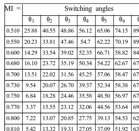
B. Structure and Principle of Operation of
F i gu r e 3 sh o ws t h e
Parrallel BMVSI
Figure 3.Proposed binary multilevel voltage source inverter (BMVSI) topolagy.
vo lt age o f e ach BM VSI h as 22+ 1-1 = 7 st ep out p ut vo ltage o ver h alf fu ndament al cycle. By means of this configuration the output voltage of p h ase e A, i.e . eA an d it s cu rr en t , i.e. iA
become respectively:
(5) eA = ________
ea1+ ea2
2
(6) iA = ia1+ ia2
wh ere ea 1, ea 2, ia 1an d ia 2are respect ively t h e
output voltages and currents of each BMVSI in p h a se s A . ea 1 a n d ea 2 a r e t h e su m o f
co r resp o n d in g cascade d n F BI u n it o u t p u t voltages, i.e.:
(7) eal =
k=1 n
S V1bk
(8) ea2 =
k=1 n
SV2bk
wh ere V1b kan d V2 bk are o u tp u t vo ltages o f
FBIs and depending switching strategy of FBIs, their values in general case will be + 2k-1V
dc, 0,
-2k-1Vdc and for Figure 3 as n=2: + Vdc, 0, +
Vd c o r + 2Vdc, 0 , -2Vdc. By a p p ro p riat e ly
turning on and off of different switching devices as illust rat ed in F igure 4( c) an d Figu re 4(f) ea l
an d ea 2 b e co me 7 st ep o u t p u t vo l t a ge s,
therefore from Equation 5, eA becomes 2(23-1)
-1 = 13 st ep s o u tp u t vo ltage as it is seen in F ig u r e 4 ( g) a lo n g wi t h it s f u n d ame n t al co m p o n e n t ( i n g e n e r a l c a s e eA i s
2(2n+1-1)-1=2 n+2-3 steps output voltage). With
re fe re n ce t o F igu re 3 , t h e cu rre n t sh arin g react o r con sists o f two magn et ically 0.5 mH co u p l e d i n d u ct o r s t h a t e q u a li z e t h e instantaneous currents ia1 and ia2 [9]. e.g. if the
current ia1tends to increase over the current ia2,
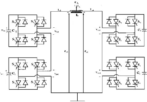
Figu re 4.T ypical output wa ve form s for proposed configura tion of SV G: (a )-T he volt age V1 b1. (b)-The voltage V1b2.
(c)-The voltage ea1. (d)-The voltage V2b1. (e)-The voltage V2b2. (f)-The voltage ea2. (g)-The voltage eAand its fundamental
component. (h)-The voltage across the current sharing inductor L.
un b alan ced cu rr en t wh ich mak es cu rren t ia1
decrease and ia 2in cr ease. At th e t ime wh en
curr ent ia 1an d ia 2are balan ced, n o emf in t h e
windings of the reactor is generated. Therefore, each side of the reactor carries half of the line cu rr en t o f t h e SVG . F igu re 4 (h ) sh o ws t h e voltage across the pole terminals of the sharing inductor L. Table 3 lists 13 levels of the output vo lt ages eA an d t h eir co r re sp o n din g swit ch
states for single-phase configuration of Figure 3 over one half fundamental cycle. The waveform of eA, illu strated in F igu re 4( g) co nt ain s o dd
harmonics of the fundamental waveform i.e.:
(9) eA =
k=1
È
S E2k-1sin [(2k-1)wt]
where E2k-1is the amplitude of (2k-1)th output
harmonic (k =1, 2, 3, ...):
(10) E2k-1= _______
i=1 N
Scos[(2k-1)qi]
2Vdc
(2k-1)p
wit h N= 2n + 1-2, in a 13-le vel SVG , n= 2 an d
N= 6. T he swit ching timin g an glesqi( i= 1, 2, ..,
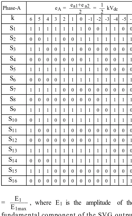
TABLE 3. Thirteen Le vels of the Output Vol tage an d th ei r Corres pond ing Switch S tates for S in gle -Ph ase Configuration of SVG Over a Half Fundamental Cycle.
eA= ________ = __ kVea1+ea2 dc
2 1 2 Phase-A -6 -5 -4 -3 -2 -1 0 1 2 3 4 5 6 k 0 0 1 1 0 0 1 1 1 1 1 1 1 S1 1 1 1 1 1 1 1 0 0 1 1 0 0 S2 0 0 0 0 0 0 0 1 1 0 0 1 1 S3 1 1 0 0 1 1 0 0 0 0 0 0 0 S4 0 0 0 0 1 1 1 1 1 1 1 1 1 S5 1 1 1 1 1 1 1 1 1 0 0 0 0 S6 0 0 0 0 0 0 0 0 0 1 1 1 1 S7 1 1 1 1 0 0 0 0 0 0 0 0 0 S8 0 1 1 0 0 1 1 1 1 1 1 1 1 S9 1 1 1 1 1 1 1 1 0 0 1 1 0 S10 0 0 0 0 0 0 0 0 1 1 0 0 1 S11 1 0 0 1 1 0 0 0 0 0 0 0 0 S12 0 0 0 1 1 1 1 1 1 1 1 1 1 S13 1 1 1 1 1 1 1 1 1 1 0 0 0 S14 0 0 0 0 0 0 0 0 0 0 1 1 1 S15 1 1 1 0 0 0 0 0 0 0 0 0 0 S16
= _____E1 , where E1 is the amplitude of the
E1max
fu n damen tal co mpo n en t o f th e SVG o u t pu t phase voltage:
6
(11) E1= ____
S
cos (qi)2Vdc
p i=1
E1maxis the maximum obtainable amplitude i.e.
th e amp lit ud e o f th e ph ase vo ltage when all swit ch in g an gles qi are eq u al t o zer o , fro m
Equation 11 it becomes: E1max= ___12 Vdc.
p
T h e anglesqi can be varied to co n tr o l t h e
fu n damen tal o u tp u t vo ltage o f t h e SVG , and also min imize t h e d ist or tio n. F o r 1 3 level in th ree-ph ase syst em 5t h , 7th , 11t h , 13t h, 17t h output voltage harmonics can be chosen.
T o ge ner at e r equ ired re act ive p o wer from
SVG , mo d u la t io n in d e x M I is va rie d an d swit ch in g t imin g an gles qi( i= 1, 2, ..., 6) ar e
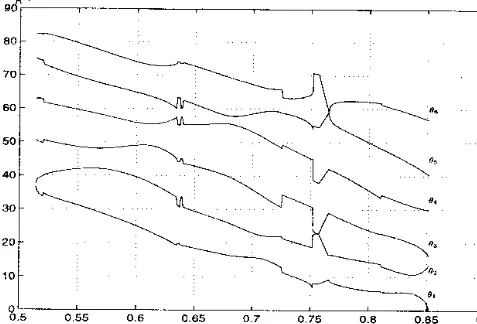
calculated for each MI value. Due to nonlinear and t ran sce n den t al ch aract erist ics, fo r each given M I, E q u at ion 10 h as to b e nu mer ically so lve d fo r swit ch in g a n gl es qi a n d gr e at
attention must be paid to the initial values of qi
usin g Newt on -R aph so n nu merical t echn iqu e. Using suitable inital conditions the solution for ab o ve men t io n ed e q u a t io n s fo r p o ssi b le modulation index varying from 0.515 to 0.851 in step s of 0.001 are o btain ed an d th e resu lts are illu st rat ed in Figu re 5. It is seen in th is figu re that for some values of MI instead of harmonic elimin at io n o n ly h armo n ic min imizat io n is p o ssib le , i.e . M I = 0. 63 an d 0.7 6 . W h e n MI= 0.851 th e SVG gen erates rated cap acitive react ive p o wer an d wh en MI = 0.515 it absorb s rated inductive power. From Figure 5 it is seen th at switch in g an gles qi a re mini mu me fo r
MI = M Ima x, t h er efo r e t h ese qi ar e u sed t o
calcu late capacitance values. The SVG cu rrent
iAeither leads or lags the phase voltage eAby__p,
2 t h e re fo r e t h e a ver ag e ch ar ge t o e ach d c cap acito r o ver every h alf cycle is equ al to zero an d b ecau se o f t h is symme tr ic ch arge flo w, vo lt ag es o n all t h e dc ca p acit o r s r e main theoritcally balanced.
However, because of the power losses in the SVG , cap acito r voltages dr ift away fro m t heir set levels. In case of the BMVSI in Figure 3, the set voltage levels are Vdc and 2Vdc. In principle,
th e charge an d hen ce th e vo lt age across each ca p acit o r is ma in t ain ed b y p r o lo n gin g o r shortening the current flow through it. This is achieved by shifting the switching patterns. The directio n of p hase shift dep ends u po n wh eth er t h e in ver t e r is p ro d u cin g le ad in g var s o r absorbing lagging vars.
MODELINGAND SIMULATIONRESULTS
å
qiFigure 5. Variations of qi(i = 1, 2, ..., 6) as a function of MI.
BMVSI seen in Figu re 1. This co nfiguration is used for the test system to illustrate three-phase simulation results.
The three-phase, 15-level VSI of Figure 6 is con nected via a co up lin g transfo rmer to an ac syst em as sh o wn in F igu r e 7 . F o r examp le, con sid er th e to tal imp edance o n th e ac side o f 13.8kV t o be 20% with 100M VA sh ort circu it level, the dc side is rated with Vdc=1.732kV, i.e.
1.732, 3.464 an d 6.928k V t o su p po rt 3 F BIs in each phases. Using the switching pattern shown in T ab le 2 with M I= 0.73 an d t h e swit ch in g timin g an glesqias: (9 .54, 20. 07, 26.70, 39.37,
52.34, 58.38, 67.49o) th e o ut p ut voltage will b e
equal to the ac system voltage, i.e. V1=13.8kV,
an d t h e r eact ive p o we r exch an ge b et we en 15-level VSI and the ac system will be zero. By varying the amplitude of the three-phase output voltage produced by 15 level VSI using different
values of MI above and below 0.73, the inverter generates or absorbs reactive power from the ac system (×Qc). The system shown in Figure 7 is
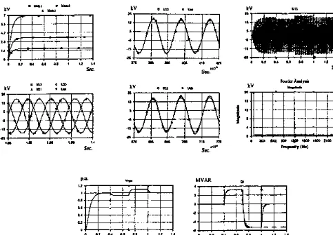
sim u la t e d u si n g t h e P S C A D / E M T D C , simu l at i o n p ro gr a m. T h e r e su lt s o f t h e simu lat io n ar e sh o wn in F igu res 8 an d 9. In Figure 8 the output line voltages of the 15-level VSI, U1 2, U23, U31, t he sp ectru m of harmo nics
presen t in U12, Qcreact ive p ower p rod uced b y
th at, t oget her wit h line syst em vo lt age Uab, 3
bin ary d c inp u t vo lt ages an d also rms valu e of the inverter output voltage Vrmsare illustrated.
It is se en t h at t h e ou t p u t vo lt age is almo st distortion-free. The produced reactive power of th e inverter was st epp ed at t1= 0.4, t2= 0.7 and
t3= 1s using differen t triggering con t ro l an gles,
qifrom Table 2 when MI is respectively 0.68, 0.8
Figure 6.Three-phase star connection of (BMVSI).
Fi gure 7.A T hre e -pha se 15 leve l V S I conne cte d to A 13.8kV power system.
valu es o f t h e ou t p ut vo ltages o f th e in ve rter wh ich creat e t h e d yn amic capab ility o f t h is compensator, are shown in this figure, e.g. at t2
= 0.7s, t his 15-level VSI is cap ab le of mak in g
almost 9 MVAR change in less than 0.1 second. Similarly, t he real p o wer exch ange bet ween the inverter and the ac system can be controlled by p hase sh ift ing t he invert er o ut p u t vo ltage wit h resp ect to t he syst e m vo lt age, i.e ., t h e inverter supplies real power to the ac system, if the inverter voltage output is made to lead the corr espo n din g ac system vo ltage. By th e same token, the inverter absorbs real power from the ac system, if the inverter output voltage is made to lag the ac system voltage. Figure 9 shows the abilit y o f t h e 15-level VSI t o mak e a 50 M W tran sit io n in a few cycles b y leadin g o r laggin g the output line voltage U12 by 30o with respect
t o t h e syst e m vo l t age Ua b. T h e in ve r t e r
th ree-p h ase cu r ren ts when t he o u tp u t act ive p o we r o f t h e in ve rt e r is 26 M W a r e also illustrated in this figure.
Figure 8.Simulation results showing the capability of 15 level VSI to establish positive and negative reactive power flow.
sin gle-p h ase t o gro u n d fau lt at lo ad b u s ar e sh o wn in F igur e 1 0. T h e fau lt p at h h as zero impe dan ce . Th e lo ad is 8 MW + j1 0 MVAR . The SVG is su p plyin g 11 MVAR leading vars. Initially the capacitor voltages are maintained at 2, 4 and 8 kV levels modulating the conduction p er io d o f e ach ca p acit o r t o co n t r o l t h eir vo ltages in a b in ar y p r op o rt io n . T h e r esu lts co n firm t h e ab ilit y o f SV G t o d yn amically comp ensat e t he syst em an d rest ore t he system to its p refau lt st at e o n ce th e fau lt is cleared after eight cycles fault at 0.35s.
F igu re 11 sh ows t h e st ar co nn ect io n o f t h e th ree-ph ase st ru ctur e o f t he p rop o sed SVG in Figure 3. This configuration is used for the test syste m t o illu str at e th r ee-p h ase simu lat io n results.
T he o per at io n al p erfo rman ce of t h e t hr ee
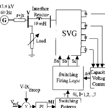
p hase 13 leve l in verte r b ased SVG sh o wn in Figure 11 was evaluated using PSCAD/EMTDC simu lat io n p ro gram. A mo de l dist rib u t io n system is shown in Figure 12 which includes the abo ve men t io n ed SVG directly co u p led t o a station bus. A remote varying load is connected through a distribution feeder.
Th e distribu tio n system co nsid erd is 13.8kV, 60Hz wit h sh o rt circu it cap acity o f 100M VA. With n or malized p er u n it mo du latio n in de x MI = 0 .7 t h e swit ch in g t imin g an gle s qi ar e
(1 4.265, 2 4.070 , 3 7.800 , 53.576 , 57 .86 6 an d 66.297o) and d c sid e voltages rat ed at 4.214kV
Figure 9. Simulation results showing the ability of 15 level VSI to create positive and negative power flow.
Figu re 11. T hre e-ph ase st a r con nect ion of pr opo se d
transformer-less binary multilevel converter (SVG).
Figure 12.Three-phase 13 level SVG connected to a 13.8
kV power system.
varying the amplitude of the three-phase output vo lt ag e p r o d u ce d b y 1 3-le ve l SV G u si n g different values of MI above and below 0.7, the SVG is capable to gen erate o r ab sorb react ive
Figure 13.Bus volt age variation with ste p change s in the
load demand without connection of compensator.
po wer fro m ac syst em. In F igu r e 12 a spe cial algor it hm wh ich p ro vid es active co n tro l o ver each capacit o r vo lt ages is used. Th e capacito r vo lt ages are co mp ared to th eir cor respo n din g referan ce voltage and an error sign al which is fi lt e re d an d u sed t o p h ase sh ift a sp ecific p o r t io n o f t h e SV G o u t p u t vo lt ag e. Th e dir ect io n o f t h e p h ase sh ift d ep en d s u p o n wh et h e r t h e SV G is pr o d u ct in g le adin g o r lagging vars. The capacitor controller is disabled wh en t he SVG's cu rren t o u tp ut is ver y lo w in magnitu de . T o regu lat e th e lo ad bu s vo lt age, pro po rt ion al plus int egral ( PI) co nt roller with feedback signal derived from the voltage at load bus (V) and the reactive current (I) flowing into the SVG weighted with V-I characteristic droop i.e. Kdroop =1% is employed. The output of the
PI controller is the modulation index (MI) and depen din g u p on its valu e, th e switch in g t imin g angles q1,q2, q3,q4, q5 and q6, to turn on and off
va ri o u s swit ch e s a r e se l e ct e d fr o m t h e p reco mp u t ed swit ch in g p att er n s tab le. T h e capacitor voltage controller generates Dqi.
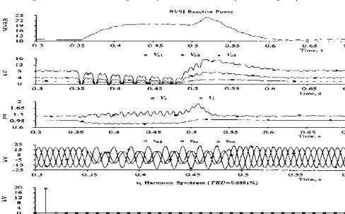
Figure 14.Simulation results showing the dynamic capabiliitly of 13 level SVG in power system environment.
appropriate gate firing pulses Sa, Sb and Sc.
P SCAD/E MTD C simu lat io n resu lts o f t h e pro p osed system are sho wn in Figures 13 and
syst em vo lt age d r o p s co r r esp o n d in g t o t h e valu es o f t h e lo ad ch anges with o u t th e SVG. Bu t wh e n SVG is u se d , fo r t h e same ste p chan ge s, th e ou tp u t system vo lt age dro ps and restored rapidly as seen in Figure 14. The phase vo ltages o f SVG alon g wit h t h e sp ectr o m o f harmo n ics pr esen t in lin e vo lt age o f SVG ar e also sh o wn in t h is figu re. It is se en t h at t h e outpot voltage of this SVG is almost distortion free . Th e vo ltages o n e ach side o f t h e dc b us capacitor and also the voltage across the current sharing inductor L for phase A is also illustrated in this figure. These simulation results show the e f f e c t i v e n e s s o f t h e p r o p o s e d S V G configuration and also the switching strategy, in o t h er wo r ds it is a go o d t o o l fo r d yn ami c compensation of a distribution system and it can be u sed for dynamic stability imp ro vemen t o f the power systems.
CONCLUSIONS
In t h is p ap er , a n ew SV G u sin g p ar alle l co nn e ct io n s o f BMVSI by mean s o f cu r ren t sh a rin g re act o rs is in t ro du ced . F o r lar ger ca p a ci t y o f p o wer syst e m co mp en sa t i o n paralleling t h e BMVSI wo u ld be pro mising for high vo lt age h igh p o we r app licatio n s. Usin g ap pro priate switching strategy, the lo wer o rd er harmo nics in th e o ut pu t o f the pro p osed SVG ar e e l i mi n a t e d , t h e r e f o r e d yn a m ic a l co mpen sation of a dist ribut ion system b eco mes po ssible wit ho ut creat in g ad itio n al harmo n ic pollution for power systems environment.
REFERENCES
1. M o ri, S . K at su hiko , M., T ake da, M . a nd Se to , M., "Development of A Large Static VAR Generator Using Se lf-Com m u ta t ed In ver t er s for Im p rovin g P owe r System Stability",IEEE Transaction of Power Sytems, Vol. 8, No. 1, (February 1993), 371-377.
2. Gyugyi, L., "Unified Power-Flow Control Concept for Flexible AC Transmition Systems", IEE Proc. C, Vol. 139, No.4, (July 1992), 323-331.
3. Gyugyi, L., "Dynamic Compensation of AC Transmission Lines by Solid-Stat e Synchronou s Volta ge Sources",
IEEE Trans action on Power D elivery, V ol. 9, N o. 2, (April 1994), 904-911.
4. Gyugyi, L., Colin, D. S. and Kalyan, K. S., "Static Sync hro nou s S er ies Com p en sa t or: A So lid -St a te Approach to the Series Compensation of Transmission Lines",IEEE Transaction on Power Delivery, Vol 12, No. 1, (January 1997), 406-417.
5. Lai, J. S. and Zheng Peng, F., "Multilevel Converters-A New Breed of Power Converters", IEEE Transaction on Industry Applications, Vol. 32, No. 3, (May/June 1996), 509-517.
6. Z he ng P e ng, F . and L ai, J . S., M ckee ver , J . W . a nd VanCoevering, J., "Voltage-Source Inverter with Separate DC Sources for Static Var Generation", IEEE Tra nsaction on Indutry Applications, V ol. 32, N o. 5, (Sept./Oct. 1996), 1130-1138.
7. PSCAD/EMTDC, "Power System Simulation Software, User's Manual", Manitoba HVDC Research Center, Manitoba, Canada, 1994.
8. Hosseini, S. H. and Mathur, R. M., "A Binary Multi-Level Voltage-Source Inverter for Static VAR Generation", CCECE' 97, St. John's NF, Canada, Conf. Rec., (1997), 427-430.