Design Principles for Tamper-Resistant Smartcard Processors
Oliver K¨ommerling
Markus G. Kuhn
Advanced Digital
University of Cambridge
Security Research
Computer Laboratory
M¨
uhlstraße 7
Pembroke Street
66484 Riedelberg
Cambridge CB2 3QG
Germany
United Kingdom
[email protected]
[email protected]
Abstract
We describe techniques for extracting protected software and data from smartcard processors. This includes manual microprobing, laser cutting, fo-cused ion-beam manipulation, glitch attacks, and power analysis. Many of these methods have already been used to compromise widely-fielded conditional-access systems, and current smartcards offer little protection against them. We give examples of low-cost protection concepts that make such attacks con-siderably more difficult.
1
Introduction
Smartcard piracy has become a common occur-rence. Since around 1994, almost every type of smartcard processor used in European, and later also American and Asian, pay-TV conditional-access sys-tems has been successfully reverse engineered. Com-promised secrets have been sold in the form of il-licit clone cards that decrypt TV channels without revenue for the broadcaster. The industry has had to update the security processor technology several times already and the race is far from over.
Smartcards promise numerous security benefits. They can participate in cryptographic protocols, and unlike magnetic stripe cards, the stored data can be protected against unauthorized access. However, the strength of this protection seems to be frequently overestimated.
In Section 2, we give a brief overview on the most important hardware techniques for breaking into smartcards. We aim to help software engineers without a background in modern VLSI test tech-niques in getting a realistic impression of how phys-ical tampering works and what it costs. Based on our observations of what makes these attacks par-ticularly easy, in Section 3 we discuss various ideas
for countermeasures. Some of these we believe to be new, while others have already been implemented in products but are either not widely used or have de-sign flaws that have allowed us to circumvent them.
2
Tampering Techniques
We can distinguish four major attack categories: • Microprobingtechniques can be used to access the chip surface directly, thus we can observe, ma-nipulate, and interfere with the integrated circuit. • Software attacks use the normal communica-tion interface of the processor and exploit secu-rity vulnerabilities found in the protocols, cryp-tographic algorithms, or their implementation. • Eavesdropping techniques monitor, with high
time resolution, the analog characteristics of all supply and interface connections and any other electromagnetic radiation produced by the pro-cessor during normal operation.
• Fault generationtechniques use abnormal en-vironmental conditions to generate malfunctions in the processor that provide additional access. All microprobing techniques areinvasive attacks. They require hours or weeks in a specialized labora-tory and in the process they destroy the packaging. The other three are non-invasive attacks. After we have prepared such an attack for a specific proces-sor type and software version, we can usually repro-duce it within seconds on another card of the same type. The attacked card is not physically harmed and the equipment used in the attack can usually be disguised as a normal smartcard reader.
Non-invasive attacks are particularly dangerous in some applications for two reasons. Firstly, the Proceedings of the USENIX Workshop on Smartcard
Technol-owner of the compromised card might not notice that the secret keys have been stolen, therefore it is unlikely that the validity of the compromised keys will be revoked before they are abused. Secondly, non-invasive attacks often scale well, as the neces-sary equipment (e.g., a small DSP board with special software) can usually be reproduced and updated at low cost.
The design of most non-invasive attacks requires detailed knowledge of both the processor and soft-ware. On the other hand, invasive microprobing at-tacks require very little initial knowledge and usually work with a similar set of techniques on a wide range of products. Attacks therefore often start with in-vasive reverse engineering, the results of which then help to develop cheaper and faster non-invasive at-tacks. We have seen this pattern numerous times on the conditional-access piracy market.
Non-invasive attacks are of particular concern in applications where the security processor is primar-ily required to providetamper evidence, while inva-sive attacks violate thetamper-resistance character-istics of a card [1]. Tamper evidence is of primary concern in applications such as banking and digi-tal signatures, where the validity of keys can easily be revoked and where the owner of the card has al-ready all the access that the keys provide anyway. Tamper resistance is of importance in applications such as copyright enforcement, intellectual property protection, and some electronic cash schemes, where the security of an entire system collapses as soon as a few cards are compromised.
To understand better which countermeasures are of practical value, we first of all have to understand the techniques that pirates have used so far to break practically all major smartcard processors on the market. In the next section, we give a short guided tour through a typical laboratory of a smartcard pi-rate.
2.1
Invasive Attacks
2.1.1 Depackaging of Smartcards
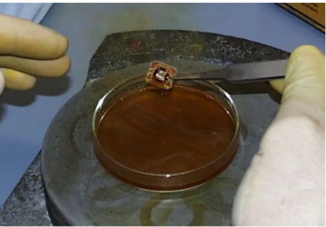
Invasive attacks start with the removal of the chip package. We heat the card plastic until it becomes flexible. This softens the glue and the chip mod-ule can then be removed easily by bending the card. We cover the chip module with 20–50 ml of fuming nitric acid heated to around 60◦C and wait for the black epoxy resin that encapsulates the silicon die to completely dissolve (Fig. 1). The procedure should preferably be carried out under very dry conditions, as the presence of water could corrode exposed alu-minium interconnects. The chip is then washed with
Figure 1: Hot fuming nitric acid (> 98% HNO3) dissolves the package without affecting the chip.
Figure 2: The depackaged smartcard processor is glued into a test package, whose pins are then con-nected to the contact pads of the chip with fine alu-minium wires in a manual bonding machine.
acetone in an ultrasonic bath, followed optionally by a short bath in deionized water and isopropanol. We remove the remaining bonding wires with tweezers, glue the die into a test package, and bond its pads manually to the pins (Fig. 2). Detailed descriptions of these and other preparation techniques are given in [2, 3].
2.1.2 Layout Reconstruction
The next step in an invasive attack on a new pro-cessor is to create a map of it. We use an optical microscope with a CCD camera to produce several meter large mosaics of high-resolution photographs of the chip surface. Basic architectural structures, such as data and address bus lines, can be identi-fied quite quickly by studying connectivity patterns
Figure 3: Left: CMOS AND gate imaged by a con-focal microscope. Right: same gate after removal of metal layer (HF wet etching). Polysilicon intercon-nects and diffusion areas are now fully visible.
and by tracing metal lines that cross clearly visible module boundaries (ROM, RAM, EEPROM, ALU, instruction decoder, etc.). All processing modules are usually connected to the main bus via easily rec-ognizable latches and bus drivers. The attacker ob-viously has to be well familiar with CMOS VLSI design techniques and microcontroller architectures, but the necessary knowledge is easily available from numerous textbooks [4, 5, 6, 7].
Photographs of the chip surface show the top metal layer, which is not transparent and therefore obscures the view on many structures below. Un-less the oxide layers have been planarized, lower layers can still be recognized through the height variations that they cause in the covering layers. Deeper layers can only be recognized in a second se-ries of photographs after the metal layers have been stripped off, which we achieve by submerging the chip for a few seconds in hydrofluoric acid (HF) in an ultrasonic bath [2]. HF quickly dissolves the silicon oxide around the metal tracks and detaches them from the chip surface. HF is an extremely dangerous substance and safety precautions have to be followed carefully when handling it.
Figure 3 demonstrates an optical layout recon-struction of a NAND gate followed by an inverter. These images were taken with a confocal micro-scope (Zeiss Axiotron-2 CSM), which assigns differ-ent colors to differdiffer-ent focal planes (e.g., metal=blue, polysilicon=green) and thus preserves depth infor-mation [8]. Multilayer images like those shown in Fig. 3 can be read with some experience almost as easily as circuit diagrams. These photographs help us in understanding those parts of the circuitry that are relevant for the planned attack.
If the processor has a commonly accessible stan-dard architecture, then we have to reconstruct the
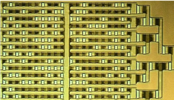
Figure 4: The vias in this structure found in a ST16F48A form a permutation matrix between the memory readout column lines and the 16:1 demulti-plexer. The applied mapping remains clearly visible.
layout only until we have identified those bus lines and functional modules that we have to manipulate to access all memory values. More recently, design-ers of conditional-access smartcards have started to add proprietary cryptographic hardware functions that forced the attackers to reconstruct more com-plex circuitry involving several thousand transistors before the system was fully compromised. How-ever, the use of standard-cell ASIC designs allows us to easily identify logic gates from their diffusion area layout, which makes the task significantly easier than the reconstruction of a transistor-level netlist.
Some manufacturers use non-standard instruction sets and bus-scrambling techniques in their secu-rity processors. In this case, the entire path from the EEPROM memory cells to the instruction de-coder and ALU has to be examined carefully before a successful disassembly of extracted machine code becomes possible. However, the attempts of bus scrambling that we encountered so far in smartcard processors were mostly only simple permutations of lines that can be spotted easily (Fig. 4).
Any good microscope can be used in optical VLSI layout reconstruction, but confocal microscopes have a number of properties that make them particularly suited for this task. While normal microscopes pro-duce a blurred image of any plane that is out of fo-cus, in confocal scanning optical microscopes, every-thing outside the focal plane just becomes dark [8]. Confocal microscopes also provide better resolution and contrast. A chromatic lens in the system can make the location of the focal plane wavelength de-pendent, such that under white light different layers
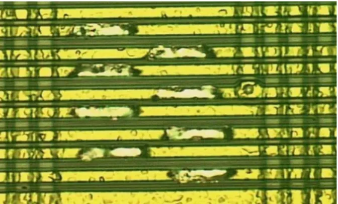
Figure 5: The data of this NOR ROM becomes clearly visible when the covering metal and polysili-con access lines plus the surrounding field oxide have been removed (HF wet etching). The image shows 16×10 bits in an ST16xyz. Every bit is represented by either a present or missing diffusion layer connec-tion.
of the chip will appear simultaneously, but in differ-ent colors.
Automatic layout reconstruction has been demon-strated with scanning electron microscopy [9]. We consider confocal microscopy to be an attractive al-ternative, because we do not need a vacuum envi-ronment, the depth information is preserved, and the option of oil immersion allows the hiding of un-evenly removed oxide layers. With UV microscopy, even chip structures down to 0.1µm can be resolved. With semiautomatic image-processing methods, significant portions of a processor can be reverse engineered within a few days. The resulting poly-gon data can then be used to automatically generate transistor and gate-level netlists for circuit simula-tions.
Optical reconstruction techniques can also be used to read ROM directly. The ROM bit pattern is stored in the diffusion layer, which leaves hardly any optical indication of the data on the chip sur-face. We have to remove all covering layers using HF wet etching, after which we can easily recognize the rims of the diffusion regions that reveal the stored bit pattern (Fig. 5).
Some ROM technologies store bits not in the shape of the active area but by modifying transistor threshold voltages. In this case, additional dopant-selective staining techniques have to be applied to make the bits visible (Fig. 6). Together with an understanding of the (sometimes slightly scrambled, see Fig. 4) memory-cell addressing, we obtain disas-sembler listings of the entire ROM content. Again, automated processing techniques can be used to ex-tract the data from photos, but we also know cases
Figure 6: The implant-mask layout of a NAND ROM can be made visible by a dopant-selective crystallographic etch (Dash etchand [2]). This im-age shows 16×14 bits plus parts of the row selec-tor of a ROM found on an MC68HC05SC2xCPU. The threshold voltage of 0-bit p-channel transistors (stained dark here) was brought below 0 V through ion implantation.
where an enthusiastic smartcard hacker has recon-structed several kilobytes of ROM manually.
While the ROM usually does not contain any cryptographic key material, it does often contain enough I/O, access control, and cryptographic rou-tines to be of use in the design of a non-invasive attack.
2.1.3 Manual Microprobing
The most important tool for invasive attacks is a microprobing workstation. Its major component is a special optical microscope (e.g., Mitutoyo FS-60) with a working distance of at least 8 mm between the chip surface and the objective lens. On a stable platform around a socket for the test package, we in-stall several micropositioners (e.g., from Karl Suss, Micromanipulator, or Wentworth Labs), which allow us to move a probe arm with submicrometer preci-sion over a chip surface. On this arm, we install a “cat whisker” probe (e.g., Picoprobe T-4-10). This is a metal shaft that holds a 10 µm diameter and 5 mm long tungsten-hair, which has been sharpened at the end into a<0.1µm tip. These elastic probe hairs allow us to establish electrical contact with on-chip bus lines without damaging them. We connect them via an amplifier to a digital signal processor card that records or overrides processor signals and also provides the power, clock, reset, and I/O signals needed to operate the processor via the pins of the test package.
On the depackaged chip, the top-layer aluminium interconnect lines are still covered by a passivation
Figure 7: This image shows 9 horizontal bus lines on a depackaged smartcard processor. A UV laser (355 nm, 5 ns) was used to remove small patches of the passivation layer over the eight data-bus lines to provide for microprobing access.
layer (usually silicon oxide or nitride), which pro-tects the chip from the environment and ion migra-tion. On top of this, we might also find a poly-imide layer that was not entirely removed by HNO3 but which can be dissolved with ethylendiamine. We have to remove the passivation layer before the probes can establish contact. The most convenient depassivation technique is the use of a laser cutter (e.g., from New Wave Research).
The UV or green laser is mounted on the camera port of the microscope and fires laser pulses through the microscope onto rectangular areas of the chip with micrometer precision. Carefully dosed laser flashes remove patches of the passivation layer. The resulting hole in the passivation layer can be made so small that only a single bus line is exposed (Fig. 7). This prevents accidental contacts with neighbouring lines and the hole also stabilizes the position of the probe and makes it less sensitive to vibrations and temperature changes.
Complete microprobing workstations cost tens of thousands of dollars, with the more luxurious ver-sions reaching over a hundred thousand US$. The cost of a new laser cutter is roughly in the same region.
Low-budget attackers are likely to get a cheaper solution on the second-hand market for semicon-ductor test equipment. With patience and skill it should not be too difficult to assemble all the re-quired tools for even under ten thousand US$ by buying a second-hand microscope and using self-designed micropositioners. The laser is not essential for first results, because vibrations in the probing needle can also be used to break holes into the pas-sivation.
2.1.4 Memory Read-out Techniques
It is usually not practical to read the information stored on a security processor directly out of each single memory cell, except for ROM. The stored data has to be accessed via the memory bus where all data is available at a single location. Microprobing is used to observe the entire bus and record the values in memory as they are accessed.
It is difficult to observe all (usually over 20) data and address bus lines at the same time. Various techniques can be used to get around this problem. For instance we can repeat the same transaction many times and use only two to four probes to ob-serve various subsets of the bus lines. As long as the processor performs the same sequence of mem-ory accesses each time, we can combine the recorded bus subset signals into a complete bus trace. Over-lapping bus lines in the various recordings help us to synchronize them before they are combined.
In applications such as pay-TV, attackers can eas-ily replay some authentic protocol exchange with the card during a microprobing examination. These applications cannot implement strong replay pro-tections in their protocols, because the transaction counters required to do this would cause an NVRAM write access per transaction. Some conditional-access cards have to perform over a thousand pro-tocol exchanges per hour and EEPROM technology allows only 104–106write cycles during the lifetime of a storage cell. An NVRAM transaction counter would damage the memory cells, and a RAM counter can be reset by the attacker easily by removing power. Newer memory technologies such as FERAM allow over 109 write cycles, which should solve this problem.
Just replaying transactions might not suffice to make the processor access all critical memory loca-tions. For instance, some banking cards read criti-cal keys from memory only after authenticating that they are indeed talking to an ATM. Pay-TV card designers have started to implement many different encryption keys and variations of encryption algo-rithms in every card, and they switch between these every few weeks. The memory locations of algorithm and key variations are not accessed by the proces-sor before these variations have been activated by a signed message from the broadcaster, so that passive monitoring of bus lines will not reveal these secrets to an attacker early.
Sometimes, hostile bus observers are lucky and encounter a card where the programmer believed that by calculating and verifying some memory checksum after every reset the tamper-resistance
could somehow be increased. This gives the at-tacker of course easy immediate access to all memory locations on the bus and simplifies completing the read-out operation considerably. Surprisingly, such memory integrity checks were even suggested in the smartcard security literature [10], in order to defeat a proposed memory rewrite attack technique [11]. This demonstrates the importance of training the designers of security processors and applications in performing a wide range of attacks before they start to design countermeasures. Otherwise, measures against one attack can far too easily backfire and simplify other approaches in unexpected ways.
In order to read out all memory cells without the help of the card software, we have to abuse a CPU component as an address counter to access all mem-ory cells for us. The program counter is already incremented automatically during every instruction cycle and used to read the next address, which makes it perfectly suited to serve us as an address sequence generator [12]. We only have to prevent the proces-sor from executing jump, call, or return instructions, which would disturb the program counter in its nor-mal read sequence. Tiny modifications of the in-struction decoder or program counter circuit, which can easily be performed by opening the right metal interconnect with a laser, often have the desired ef-fect.
2.1.5 Particle Beam Techniques
Most currently available smartcard processors have feature sizes of 0.5–1 µm and only two metal lay-ers. These can be reverse-engineered and observed with the manual and optical techniques described in the previous sections. For future card genera-tions with more metal layers and features below the wavelength of visible light, more expensive tools ad-ditionally might have to be used.
A focused ion beam (FIB) workstation consists of a vacuum chamber with a particle gun, comparable to a scanning electron microscope (SEM). Gallium ions are accelerated and focused from a liquid metal cathode with 30 kV into a beam of down to 5–10 nm diameter, with beam currents ranging from 1 pA to 10 nA. FIBs can image samples from secondary par-ticles similar to a SEM with down to 5 nm resolution. By increasing the beam current, chip material can be removed with the same resolution at a rate of around 0.25 µm3nA−1
s−1 [13]. Better etch rates can be achieved by injecting a gas like iodine via a needle that is brought to within a few hundred micrometers from the beam target. Gas molecules settle down on the chip surface and react with removed material to
form a volatile compound that can be pumped away and is not redeposited. Using this gas-assisted etch technique, holes that are up to 12 times deeper than wide can be created at arbitrary angles to get ac-cess to deep metal layers without damaging nearby structures. By injecting a platinum-based organo-metallic gas that is broken down on the chip surface by the ion beam, platinum can be deposited to es-tablish new contacts. With other gas chemistries, even insulators can be deposited to establish surface contacts to deep metal without contacting any cov-ering layers.
Using laser interferometer stages, a FIB operator can navigate blindly on a chip surface with 0.15µm precision, even if the chip has been planarized and has no recognizable surface structures. Chips can also be polished from the back side down to a thick-ness of just a few tens of micrometers. Using laser-interferometer navigation or infrared laser imaging, it is then possible to locate individual transistors and contact them through the silicon substrate by FIB editing a suitable hole. This rear-access technique has probably not yet been used by pirates so far, but the technique is about to become much more commonly available and therefore has to be taken into account by designers of new security chips.
FIBs are used by attackers today primarily to simplify manual probing of deep metal and polysil-icon lines. A hole is drilled to the signal line of in-terest, filled with platinum to bring the signal to the surface, where a several micrometer large prob-ing pad or cross is created to allow easy access (Fig. 11). Modern FIB workstations (for example the FIB 200xP from FEI) cost less than half a mil-lion US$ and are available in over hundred organiza-tions. Processing time can be rented from numerous companies all over the world for a few hundred dol-lars per hour.
Another useful particle beam tool are electron-beam testers (EBT) [14]. These are SEMs with a voltage-contrast function. Typical acceleration volt-ages and beam currents for the primary electrons are 2.5 kV and 5 nA. The number and energy of sec-ondary electrons are an indication of the local elec-tric field on the chip surface and signal lines can be observed with submicrometer resolution. The signal generated during e-beam testing is essentially the low-pass filtered product of the beam current mul-tiplied with a function of the signal voltage, plus noise. EBTs can measure waveforms with a band-width of several gigahertz, but only with periodic signals where stroboscopic techniques and periodic averaging can be used. If we use real-time voltage-contrast mode, where the beam is continuously
di-rected to a single spot and the blurred and noisy stream of secondary electrons is recorded, then the signal bandwidth is limited to a few megahertz [14]. While such a bandwidth might just be sufficient for observing a single signal line in a 3.5 MHz smart-card, it is too low to observe an entire bus with a sample frequency of several megahertz for each line. EBTs are very convenient attack tools if the clock frequency of the observed processor can be reduced below 100 kHz to allow real-time recording of all bus lines or if the processor can be forced to generate periodic signals by continuously repeating the same transaction during the measurement.
2.2
Non-invasive Attacks
A processor is essentially a set of a few hundred flipflops (registers, latches, and SRAM cells) that de-fine its current state, plus combinatorial logic that calculates from the current state the next state dur-ing every clock cycle. Many analog effects in such a system can be used in non-invasive attacks. Some examples are:
• Every transistor and interconnection have a ca-pacitance and resistance that, together with fac-tors such as the temperature and supply voltage, determine the signal propagation delays. Due to production process fluctuations, these values can vary significantly within a single chip and between chips of the same type.
• A flipflop samples its input during a short time interval and compares it with a threshold volt-age derived from its power supply voltvolt-age. The time of this sampling interval is fixed relative to the clock edge, but can vary between individual flipflops.
• The flipflops can accept the correct new state only after the outputs of the combinatorial logic have stabilized on the prior state.
• During every change in a CMOS gate, both the p- and n-transistors are open for a short time, creating a brief short circuit of the power supply lines [15]. Without a change, the supply current remains extremely small.
• Power supply current is also needed to charge or discharge the load capacitances when an output changes.
• A normal flipflop consists of two inverters and two transmission gates (8 transistors). SRAM cells use only two inverters and two transistors
to ground one of the outputs during a write oper-ation. This saves some space but causes a signif-icant short-circuit during every change of a bit. There are numerous other effects. During careful security reviews of processor designs it is often nec-essary to perform detailed analog simulations and tests and it is not sufficient to just study a digital abstraction.
Smartcard processors are particularly vulnerable to non-invasive attacks, because the attacker has full control over the power and clock supply lines. Larger security modules can be equipped with backup bat-teries, electromagnetic shielding, low-pass filters, and autonomous clock signal generators to reduce many of the risks to which smartcard processors are particularly exposed.
2.2.1 Glitch Attacks
In a glitch attack, we deliberately generate a mal-function that causes one or more flipflops to adopt the wrong state. The aim is usually to replace a sin-gle critical machine instruction with an almost ar-bitrary other one. Glitches can also aim to corrupt data values as they are transferred between registers and memory. Of the many fault-induction attack techniques on smartcards that have been discussed in the recent literature [11, 12, 16, 17, 18], it has been our experience that glitch attacks are the ones most useful in practical attacks.
We are currently aware of three techniques for cre-ating fairly reliable malfunctions that affect only a very small number of machine cycles in smartcard processors: clock signal transients, power supply transients, and external electrical field transients.
Particularly interesting instructions that an at-tacker might want to replace with glitches are condi-tional jumps or the test instructions preceding them. They create a window of vulnerability in the process-ing stages of many security applications that often allows us to bypass sophisticated cryptographic bar-riers by simply preventing the execution of the code that detects that an authentication attempt was un-successful. Instruction glitches can also be used to extend the runtime of loops, for instance in serial port output routines to see more of the memory af-ter the output buffer [12], or also to reduce the run-time of loops, for instance to transform an iterated cipher function into an easy to break single-round variant [11].
Clock-signal glitches are currently the simplest and most practical ones. They temporarily increase the clock frequency for one or more half cycles, such that some flipflops sample their input before the new
state has reached them. Although many manufac-turers claim to implement high-frequency detectors in their clock-signal processing logic, these circuits are often only simple-minded filters that do not de-tect single too short half-cycles. They can be cir-cumvented by carefully selecting the duty cycles of the clock signal during the glitch.
In some designs, a clock-frequency sensor that is perfectly secure under normal operating voltage ig-nores clock glitches if they coincide with a carefully designed power fluctuation. We have identified clock and power waveform combinations for some widely used processors that reliably increment the program counter by one without altering any other processor state. An arbitrary subsequence of the instructions found in the card can be executed by the attacker this way, which leaves very little opportunity for the program designer to implement effective coun-termeasures in software alone.
Power fluctuations can shift the threshold volt-ages of gate inputs and anti-tampering sensors rel-ative to the unchanged potential of connected ca-pacitances, especially if this occurs close to the sam-pling time of the flipflops. Smartcard chips do not provide much space for large buffer capacitors, and voltage threshold sensors often do not react to very fast transients.
In a potential alternative glitch technique that we have yet to explore fully, we place two metal needles on the card surface, only a few hundred micrometers away from the processor. We then apply spikes of a few hundred volts for less than a microsecond on these needles to generate electrical fields in the sil-icon substrate of sufficient strength to temporarily shift the threshold voltages of nearby transistors.
2.2.2 Current Analysis
Using a 10–15 Ω resistor in the power supply, we can measure with an analog/digital converter the fluctu-ations in the current consumed by the card. Prefer-ably, the recording should be made with at least 12-bit resolution and the sampling frequency should be an integer multiple of the card clock frequency.
Drivers on the address and data bus often con-sist of up to a dozen parallel inverters per bit, each driving a large capacitive load. They cause a sig-nificant power-supply short circuit during any tran-sition. Changing a single bus line from 0 to 1 or vice versa can contribute in the order of 0.5–1 mA to the total current at the right time after the clock edge, such that a 12-bit ADC is sufficient to esti-mate the number of bus bits that change at a time. SRAM write operations often generate the strongest
signals. By averaging the current measurements of many repeated identical transactions, we can even identify smaller signals that are not transmitted over the bus. Signals such as carry bit states are of special interest, because many cryptographic key scheduling algorithms use shift operations that single out indi-vidual key bits in the carry flag. Even if the status-bit changes cannot be measured directly, they often cause changes in the instruction sequencer or mi-crocode execution, which then cause a clear change in the power consumption.
The various instructions cause different levels of activity in the instruction decoder and arithmetic units and can often be quite clearly distinguished, such that parts of algorithms can be reconstructed. Various units of the processor have their switching transients at different times relative to the clock edges and can be separated in high-frequency mea-surements.
3
Countermeasures
3.1
Randomized Clock Signal
Many non-invasive techniques require the at-tacker to predict the time at which a certain instruc-tion is executed. A strictly deterministic processor that executes the same instructioncclock cycles af-ter each reset—if provided with the same input at every cycle—makes this easy. Predictable processor behaviour also simplifies the use of protocol reaction times as a covert channel.
The obvious countermeasure is to insert random-time delays between any observable reaction and critical operations that might be subject to an at-tack. If the serial port were the only observable channel, then a few random delay routine calls con-trolled by a hardware noise source would seem suf-ficient. However, since attackers can use cross-correlation techniques to determine in real-time from the current fluctuations the currently executed in-struction sequence, almost every inin-struction be-comes an observable reaction, and a few localized delays will not suffice.
We therefore strongly recommend introducing timing randomness at the clock-cycle level. A ran-dom bit-sequence generator that is operated with the external clock signal should be used to generate an internal clock signal. This will effectively reduce the clock frequency by a factor of four, but most smartcards anyway reduce internally the 3.5 MHz provided for contact cards and the 13 MHz provided for contact-less cards.
Hardware random bit generators (usually the am-plified thermal noise of transistors) are not always
good at producing uniform output statistics at high bit rates, therefore their output should be smoothed with an additional simple pseudo-random bit gener-ator.
The probability thatnclock cycles have been exe-cuted by a card with a randomized clock signal after
cclock cycles have been applied can be described as a binomial distribution:
p(n, c) = 2−c
c
2n
c
2n+ 1
≈
r
8
πc·e−
8
c·(n−4c)2 as c→ ∞
So for instance after we have sent 1000 clock cy-cles to the smartcard, we can be fairly sure (prob-ability > 1−10−9) that between 200 and 300 of them have been executed. This distribution can be used to verify that safety margins for timing-critical algorithms—such as the timely delivery of a pay-TV control word—are met with sufficiently high proba-bility.
Only the clock signals of circuitry such as the se-rial port and timer need to be supplied directly with the external clock signal, all other processor parts can be driven from the randomized clock.
A lack of switching transients during the inactive periods of the random clock could allow the attacker to reconstruct the internal clock signal from the con-sumed current. It is therefore essential that the pro-cessor shows a characteristic current activity even during the delay phases of the random clock. This can be accomplished by driving the bus with ran-dom values or by causing the microcode to perform a write access to an unused RAM location while the processor is inactive.
3.2
Randomized Multithreading
To introduce even more non-determinism into the execution of algorithms, it is conceivable to de-sign a multithreaded processor architecture [19] that schedules the processor by hardware between two or more threads of execution randomly at a per-instruction level. Such a processor would have mul-tiple copies of all registers (accumulator, program counter, instruction register, etc.), and the combina-torial logic would be used in a randomly alternating way to progress the execution state of the threads represented by these respective register sets.
The simple 8-bit microcontrollers of smartcards do not feature pipelines and caches and the entire state is defined only by a very small number of reg-isters that can relatively easily be duplicated. The only other necessary addition would be new machine
instructions to fork off the other thread(s) and to synchronize and terminate them. Multithreaded ap-plications could interleave some of the many inde-pendent cryptographic operations needed in secu-rity protocols. For the remaining time, the auxiliary threads could just perform random encryptions in order to generate an realistic current pattern during the delay periods of the main application.
3.3
Robust Low-frequency Sensor
Bus-observation by e-beam testing becomes much easier when the processor can be clocked with only a few kilohertz, and therefore a low-frequency alarm is commonly found on smartcard processors. How-ever, simple high-pass or low-pass RC elements are not sufficient, because by carefully varying the duty cycle of the clock signal, we can often prevent the activation of such detectors. A good low-frequency sensor must trigger if no clock edge has been seen for longer than some specified time limit (e.g., 0.5 µs). In this case, the processor must not only be reset im-mediately, but all bus lines and registers also have to be grounded quickly, as otherwise the values on them would remain visible sufficiently long for a voltage-contrast scan.Even such carefully designed low-frequency detec-tors can quite easily be disabled by laser cutting or FIB editing the RC element. To prevent such simple tampering, we suggest that an intrinsic self-test be built into the detector. Any attempt to tamper with the sensor should result in the malfunction of the en-tire processor. We have designed such a circuit that tests the sensor during a required step in the nor-mal reset sequence. External resets are not directly forwarded to the internal reset lines, but only cause an additional frequency divider to reduce the clock signal. This then activates the low-frequency de-tector, which then activates the internal reset lines, which finally deactivate the divider. The processor has now passed the sensor test and can start normal operation. The processor is designed such that it will not run after a power up without a proper in-ternal reset. A large number of FIB edits would be necessary to make the processor operational without the frequency sensor being active.
Other sensor defenses against invasive attacks should equally be embedded into the normal opera-tion of the processor, or they will easily be circum-vented by merely destroying their signal or power supply connections.
3.4
Destruction of Test Circuitry
Microcontroller production has a yield of typically around 95%, so each chip has to be thoroughly tested
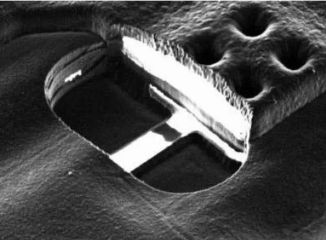
Figure 8: The interrupted white line at the bot-tom of the cavity in this FIB secondary-electron im-age is a blown polysilicon fuse next to a test pad (MC68HC05SC2xprocessor).
after production. Test engineers —like microprobing attackers—have to get full access to a complex cir-cuit with a small number of probing needles. They add special test circuitry to each chip, which is usu-ally a parallel/serial converter for direct access to many bus and control lines. This test logic is acces-sible via small probing pads or multiplexed via the normal I/O pads. On normal microcontrollers, the test circuitry remains fully intact after the test. In smartcard processors, it is common practice to blow polysilicon fuses that disable access to these test cir-cuits (Fig. 8). However, attackers have been able to reconnect these with microprobes or FIB editing, and then simply used the test logic to dump the en-tire memory content.
Therefore, it is essential that any test circuitry is not only slightly disabled but structurally destroyed by the manufacturer. One approach is to place the test interface for chipnonto the area of chipn+ 1 on the wafer, such that cutting the wafer into dies severs all its parallel connections. A wafer saw usu-ally removes a 80–200µm wide area that often only contains a few process control transistors. Locat-ing essential parts of the test logic in these cut areas would eliminate any possibility that even substantial FIB edits could reactivate it.
3.5
Restricted Program Counter
Abusing the program counter as an address pat-tern generator significantly simplifies reading out the entire memory via microprobing or e-beam testing.
Separate watchdog counters that reset the proces-sor if no jump, call, or return instruction is executed
for a number of cycles would either require many transistors or are too easily disabled.
Instead, we recommend simply not providing a program counter that can run over the entire ad-dress space. A 16-bit program counter can easily be replaced with the combination of a say 7-bit off-set counterO and a 16-bit segment registerS, such that the accessed address isS+O. Instead of over-flowing, the offset counter resets the processor after reaching its maximum value. Every jump, call, or re-turn instruction writes the destination address into
S and resetsO to zero. The processor will now be completely unable to execute more than 127 bytes of machine code without a jump, and no simple FIB edit will change this. A simple machine-code post-processor must be used by the programmer to insert jumps to the next address wherever unconditional branches are more than 127 bytes apart.
With the program counter now being unavailable, attackers will next try to increase the number of it-erations in software loops that read data arrays from memory to get access to all bytes. This can for in-stance be achieved with a microprobe that performs a glitch attack directly on a bus-line. Programmers who want to use 16-bit counters in loops should keep this in mind.
3.6
Top-layer Sensor Meshes
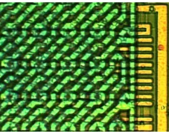
Additional metallization layers that form a sen-sor mesh above the actual circuit and that do not carry any critical signals remain one of the more effective annoyances to microprobing attack-ers. They are found in a few smartcard CPUs such as the ST16SF48A or in some battery-buffered SRAM security processors such as the DS5002FPM and DS1954.
A sensor mesh in which all paths are continu-ously monitored for interruptions and short-circuits while power is available prevents laser cutter or se-lective etching access to the bus lines. Mesh alarms should immediately trigger a countermeasure such as zeroizing the non-volatile memory. In addition, such meshes make the preparation of lower layers more difficult, because since the etch progresses un-evenly through them, their pattern remains visible in the layers below and therefore they complicate automatic layout reconstruction. Finally, a mesh on top of a polished oxide layer hides lower layers, which makes navigation on the chip surface for probing and FIB editing more tedious.
The implementations of sensor meshes in fielded products however show a number of quite surpris-ing design flaws that significantly reduce the protec-tion (Fig. 9 and 10). The most significant flaw is
Figure 9: Escape route for imprisoned crypto bits: The ST16SF48A designers generously added this re-dundant extension of the bus several micrometers beyond the protected mesh area, providing easy probing access.
Figure 10: Every second line is connected to VCC or GND at one end and open at the other. Not all are used to supply lower layers and therefore some can safely be opened with a laser for probing access to the bus lines below.
that a mesh breach will only set a flag in a status register and that zeroization of the memory is left completely to the application software. We noted in Section 2.1.4 that a common read-out technique involves severely disabling the instruction decoder, therefore software checks for invasive attacks are of little use.
A well-designed mesh can make attacks by man-ual microprobing alone rather difficult, and more so-phisticated FIB editing procedures will be required to bypass it. Several techniques can be applied here. The resolution of FIB drilling is much smaller than the mesh line spacings, therefore it is no problem to establish contact through three or more metal layers and make deeply buried signals accessible for
micro-Figure 11: A FIB was used here to drill a fine hole to a bus line through the gap between two sensor mesh lines, refill it with metal, and place a metal cross on top for easy microprobing access.
probing via a platinum or tungsten pad on top of the passivation layer (Fig. 11). Alternatively, it is also possible to etch a larger window into the mesh and then reconnect the loose ends with FIB metal deposits around it.
4
Conclusion
We have presented a basis for understanding the mechanisms that make microcontrollers partic-ularly easy to penetrate. With the restricted pro-gram counter, the randomized clock signal, and the tamper-resistant low-frequency sensor, we have shown some selected examples of low-cost coun-termeasures that we consider to be quite effective against a range of attacks.
There are of course numerous other more obvi-ous countermeasures against some of the commonly used attack techniques which we cannot cover in de-tail in this overview. Examples are current regula-tors and noisy loads against current analysis attacks and loosely coupled PLLs and edge barriers against clock glitch attacks. A combination of these together with e-field sensors and randomized clocks or per-haps even multithreading hardware in new processor designs will hopefully make high-speed non-invasive attacks considerably less likely to succeed. Other countermeasures in fielded processors such as light and depassivation sensors have turned out to be of little use as they can be easily bypassed.
We currently see no really effective short-term protection against carefully planned invasive tam-pering involving focused ion-beam tools. Zeroiza-tion mechanisms for erasing secrets when tampering
is detected require a continuous power supply that the credit-card form factor does not allow. The at-tacker can thus safely disable the zeroization mecha-nism before powering up the processor. Zeroization remains a highly effective tampering protection for larger security modules that can afford to store se-crets in battery-backed SRAM (e.g., DS1954 or IBM 4758), but this is not yet feasible for the smartcard package.
5
Acknowledgements
The authors would like to thank Ross Anderson, Simon Moore, Steven Weingart, Matthias Brunner, Gareth Evans and others for useful and highly inter-esting discussions.
References
[1] FIPS PUB 140-1: Security Requirements for Cryptographic Modules. National Institute of Standards and Technology, U.S. Department of Commerce, 11 January 1994.
[2] F. Beck: Integrated Circuit Failure Analysis – A Guide to Preparation Techniques. John Wiley & Sons, 1998.
[3] T.W. Lee, S.V. Pabbisetty (eds.): Microelec-tronic Failure Analysis, Desk Reference. 3rd edition, ASM International, Ohio, 1993, ISBN 0-87170-479-X.
[4] N.H.E. Weste, K. Eshraghian: Principles of CMOS VLSI Design. Addison-Wesley, 1993. [5] S.-M. Kang, Y. Leblebici: CMOS Digital
Inte-grated Circuits: Analysis and Design. McGraw-Hill, 1996.
[6] J. Carter: Microprocessor Architecture and Mi-croprogramming – A State-Machine Approach. Prentice-Hall, 1996.
[7] S.M. Sze:Semiconductor Devices – Physics and Technology. John Wiley & Sons, 1985.
[8] T.R. Corle, G.S. Kino: Confocal Scanning Op-tical Microscopy and Related Imaging Systems. Academic Press, 1996.
[9] S. Blythe, et al.: Layout Reconstruction of Complex Silicon Chips.IEEE Journal of Solid-State Circuits, 28(2):138–145, February 1993. [10] D.P. Maher: Fault Induction Attacks, Tamper
Resistance, and Hostile Reverse Engineering
in Perspective. In R. Hirschfeld (ed.): Finan-cial Cryptography, FC ’97, Proceedings, LNCS 1318, pp. 109–121, Springer-Verlag, 1997. [11] R.J. Anderson, M.G. Kuhn: Low Cost
At-tacks on Tamper Resistant Devices. In M. Lo-mas, et al. (eds.),Security Protocols, 5th Inter-national Workshop, LNCS 1361, pp. 125–136, Springer-Verlag, 1997
[12] R.J. Anderson, M.G. Kuhn: Tamper Resis-tance — a Cautionary Note. In The Second USENIX Workshop on Electronic Commerce Proceedings, pp. 1–11, Oakland, California, 18– 21 November 1996.
[13] J.H. Daniel, D.F. Moore, J.F. Walker: Fo-cused Ion Beams for Microfabrication. Engi-neering Science and Education Journal, pp. 53– 56, April 1998.
[14] H. P. Feuerbaum: Electron Beam Testing: Methods and Applications. Scanning, 5(1):14– 24, 1982.
[15] H.J.M. Veendrick: Short-Circuit Dissipation of Static CMOS Circuitry and Its Impact on the Design of Buffer Circuits. IEEE Journal of Solid-State Circuits, 19(4):468–473, August 1984.
[16] D. Boneh, R.A. DeMillo, R.J. Lipton: On the Importance of Checking Cryptographic Pro-tocols for Faults. In Advances in Cryptology – EUROCRYPT ’97, LNCS 1233, pp. 37–51, Springer-Verlag, 1997.
[17] F. Bao, et al.: Breaking Public Key Cryp-tosystems on Tamper Resistant Devices in the Presence of Transient Faults. In M. Lomas, et al. (eds.), Security Protocols, 5th Interna-tional Workshop, LNCS 1361, pp. 115–124, Springer-Verlag, 1997.
[18] M. Joye, J.-J. Quisquater, F. Bao, R. H. Deng: RSA-type Signatures in the Presence of Transient Faults. In Cryptography and Cod-ing, LNCS 1355, pp. 155–160, Springer-Verlag, 1997.
[19] S.W. Moore: Multithreaded Processor Design. Kluwer Academic Publishers, 1996.