International Journal of Science Engineering and Advance Technology,
IJSEAT, Vol 2, Issue 2, February - 2014
ISSN 2321-6905
Area reduction in CSLA with efficient delay management
Ch Gayatri,Mtech (VLSI), D Naveen
Avant I institute of engineering & technology,
Asst. prof..Avanthi institute of engineering & technology,
Tagarapulasa, vizianagaram ,
[email protected], [email protected],
Abstract
Adders play a key role in the arithmetic processors. There are many ways to design an adder. The major disadvantage of digital adders are that its speed is limited due to delay occurred in carry propagation. Carry select adder (CSLA) is one of the fastest adders used in many computational systems to improve the carry propagation delay by independently generating multiple carries and then select a carry to generate the sum. But the area of CSLA increases with the use of dual RCAs. A CSLA with Binary to Excees-1 Converter (BEC) is designed to reduce the area of the CSLA, but the delay over head is increasing. To further decrease the area and to keep the delay constant or equal as basic CSLA, an add one circuit can be used to design a CSLA. This work proposes the design of 8-bit, 16-bit, 32-16-bit, 64-bit and 128-bit square root CSLA (SQRT CSLA) using BEC with significant reduction in area.
Key words- CSLA, BEC, processor. SQRT CSLA
1. Introduction
VLSI IC’s are those circuits which contain more than 105 transistors and these circuits can be used as general purpose IC’s such as microprocessors, memories, DSPs and also as Application Specific IC’s (ASICs). In VLSI technology, the main design entity is area which measures the cost and power consumption of that IC. Reduced area and high speed data path logic systems are the main areas of research in VLSI system design. High-speed addition and multiplication has always been a fundamental requirement of high-performance processors and systems.
In rapidly growing mobile industry, faster units are not the only concern but also smaller area and less power become major concerns for design of digital
circuits. In mobile electronics, reducing area and power consumption are key factors in increasing portability and battery life. Even in servers and desktop computers power dissipation is an important design constraint. Addition is the heart of computer arithmetic, and the arithmetic unit is often the work horse of a computational circuit. They are the necessary component of a data path, e.g. in microprocessors or a signal processor.
1.1 Hardware Description Language (HDL):
Hardware Description Language (HDL) is a language that can describe the behavior and structure of electronic system, but it is particularly suited as a language to describe the structure and the behavior of the digital electronic hardware design, such as ASICs and FPGAs as well as conventional circuits.HDL can be used to describe electronic hardware at many different levels of abstraction such as algorithm, Register Transfer Level (RTL) and Gate level.
HDL allows this issue to be addressed in two ways, a HDL specification can be executed in order to achieve a high level of confidence in its correctness before commencing design and may simulate one specification for a part in the wider system context ( e.g. :- Printed Circuited Board simulation).
1.2 Compilation and simulation of VHDL code:
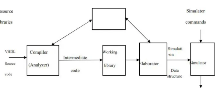
Fig 1 Compilation, Elaboration and simulation of VHDL code
The VHDL compiler, also called an analyzer, first checks the VHDL source code to see that it conforms to the syntax and semantic rules of VHDL. If there is syntax error such as a missing semicolon, or if there is a semantic error such as trying to add two signals of incompatible types, the compiler will output an appropriate error message. The compiler also checks to see that references to libraries are correct. If the VHDL code conforms to all the rules, the compiler generates intermediate code, which can be used by a simulator or by a synthesizer.
In preparation for simulation, the VHDL intermediate code must be converted to a form that can be used by the simulator. This step is referred to as elaboration. During elaboration, ports are created for each instance of a component, memory storage is allocated for the required signals, the interconnections among the port signals are specified, and a mechanism is established for executing the VHDL processes in the proper sequence.
The resulting data structure represents the digital
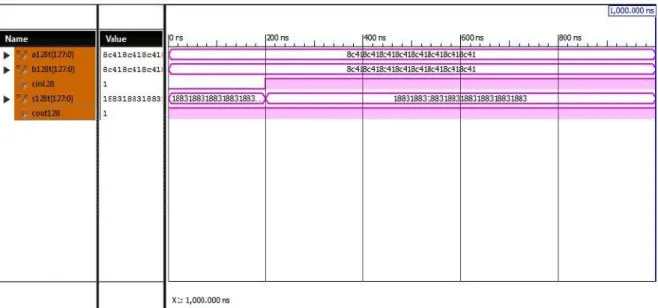
system being simulated. After an initialization phase, the simulator enters the execution phase. The simulator accepts simulation commands, which control the simulation of the digital system and specify the desired simulator output. In this work, Isim simulator is used for functional simulation. The functional simulation results of 128-bit SQRT CSLA and 128-bit SQRT CSLA with add one circuit is shown in fig 7.1 and fig 7.2 respectively.
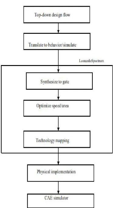
1.3 LeonardoSpectrum:
LeonardoSpectrum is a suite of high level design tools for a Complex Programmable Logic Device (CPLD), Field Programmable Gate Array (FPGA), or Application Specific Integrated Circuit (ASIC). Leonardo Spectrum offers design capture, VHDL and Verilog entry, register transfer-level debugging for logic synthesis, constraint-based optimization, timing analysis, encapsulated
place-and-route, and schematic viewing.
International Journal of Science Engineering and Advance Technology,
IJSEAT, Vol 2, Issue 2, February - 2014
ISSN 2321-6905
Fig 6.4 Top-down design flow of LeonardoSpectrum
SIMULATION AND SNYTHESIS RESULTS
result-Fig 7.1 Simulation result of 128-bit SQRT CSLA
7.1.2 128-Bit SQRT CSLA with BEC simulation
result-Fig 7.2 Simulation result of 128-bit SQRT CSLA with add one circuit
International Journal of Science Engineering and Advance Technology,
IJSEAT, Vol 2, Issue 2, February - 2014
ISSN 2321-6905
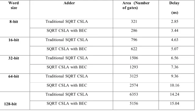
Word
size Adder Area (Numberof gates) Delay (ns) 8-bit Traditional SQRT CSLA 321 2.85
SQRT CSLA with BEC 286 3.44
16-bit Traditional SQRT CSLA 796 4.63
SQRT CSLA with BEC 622 5.07
32-bit Traditional SQRT CSLA 1506 6.56
SQRT CSLA with BEC 1293 7.36
64-bit Traditional SQRT CSLA 3125 9.36
SQRT CSLA with BEC 2574 10.16
128-bit
Traditional SQRT CSLA 6353 14.24
SQRT CSLA with BEC 5156 15.04
Table 7.1 Comparison of area and delay in between the three adders
7.2 Synthesis results: Area report of 128-bit SQRT CSLA with BEC:
Library: work Cell Library References Total Area
m12 work 1 x 83 83 Gates
m16 work 1 x 10⁹ 109 Gates
m17 work 1 x 115 112 Gates
Number of ports : 386
Number of nets : 668
Number of instances : 94
Number of references to this view : 0
Total accumulated area :
Number of gates : 5156
Number of accumulated instances : 979
7.2.2 Delay report of 128-bit SQRT CSLA with add one circuit:
Critical Path Report
Critical path #1, (constrained path)
NAME GATE ARRIVAL
LOAD
--
---b128t(2)/ 0.00 0.00 dn
0.19
ix480/X ND2N0 0.12 0.12 up
0.14
ix478/X XR3T0 0.48 0.70 dn
0.17
ix187/X NR2R0 0.50 1.20 up
0.19
ix471/X XR2T0 0.47 2.15 dn
0.11
ix197/X MX2L0 0.41 2.56 up
0.32
ix468/X MX2L0 0.91 3.47 up
0.32
ix466/X MX2L1 0.89 4.36 up
0.54
ix229/X MX2T1 0.90 5.26 up
0.69
h646/ix19/X MX2T1 1.04 6.30 up
0.79
h647/ix21/X MX2T1 1.10 7.39 up
0.72
International Journal of Science Engineering and Advance Technology,
IJSEAT, Vol 2, Issue 2, February - 2014
ISSN 2321-6905
[Type text]
Page 85
h6411_z2/ix7/X
1.11 MX2T2 0.89 11.25 up
h6412_z2/ix7/X MX2T2 0.94 12.20 up
1.27
h6413_z2/ix7/X MX2T2 1.08 13.28 up
1.76
h6414_z2/ix7/X MX2T2 1.12 14.40 up
0.86
h6415_z2/ix23/X MX2T0 0.47 14.82 dn
0.04
s128t(126)/ 0.00 14.82 dn
0.00
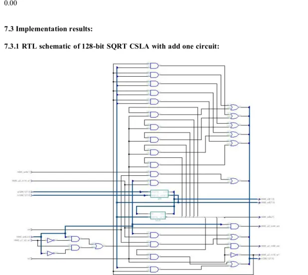
7.3 Implementation results:
7.3.1 RTL schematic of 128-bit SQRT CSLA with add one circuit:
Fig 7.3 RTL schematic for 128-bit Carry Select Adder with BEC
32-SQRT CSLA with BEC logic are evaluated and compared with the proposed SQRT CSLA with BEC. It is clear from table- that, the proposed adder takes less delay and area when compared with SQRT CSLA. It is also observed that in the proposed adder the reduction in area is very high with insignificant penalty in the delay when compared with traditional SQRT CSLA.As the input length is progressed the area is decreased in the same proportion, but in the same proportion the delay penalty is not increased. Since the area in the proposed adder is very less, it is obvious that, the power consumption is also very less. Therefore this adder can be preferred for low power applications.
References
[1] O. J. Bedrij, “Carry-select adder,” IRE Trans. Electron. Comput.,pp.340–344, 1962. [2] Y. Kim and L.-S. Kim, “64-bit carry-select adder with reduced area,”Electron. Lett., vol. 37, no. 10, pp. 614–615, May 2001.
[3] B. Ramkumar, H.M. Kittur, and P. M. Kannan, “ASIC implementation of modified faster carry save adder,” Eur. J. Sci. Res., vol. 42, no. 1, pp. 53–58, 2010.
[4] T. Y. Ceiang and M. J. Hsiao, “Carry-select adder using single ripple carry adder,” Electron. Lett., vol. 34, no. 22, pp. 2101–2103, Oct. 1998. [6] Y. He, C. H. Chang, and J. Gu, “An area efficient 64-bit square root carry-select adder for low power applications,” in Proc. IEEE Int. Symp. Circuits Syst., 2005, vol.4, pp. 4082– 4085.
[7] B. Ramkumar and Harish M Kittur, “Low-Power and Area-Efficient Carry Select
Adder” IEEE transactions on very large scale integration (VLSI) systems, vol. 20, no. 2, February 2012]
[8] N. Weste and K. Eshragian, Principles
of CMOS VLSI Designs: A System
Perspective, 2nd ed., Addison-Wesley, 1985-1993.
[9] Morinaka, H., Makino, H., Nakase, Y. et.
using Modified Carry Select". Cz/stoin Integrated Circuit Conference, 1995, pages 585-588
[10] Milos D. Ercegovac and Thomas Lang, “Digital arthimetic,” Morgan Kaufmann, Elsevier INC, 2004.
[11] W.Jeong and K.Roy, “robust high-performance low power adder”,proc,of the Asia and South Pacific Design Automatin Conference,pp.503-506,2003
[12] D.C Chen, L. M. Guerra,E. H. Ng, M. Potkonjak, D.P. Schultz and J. M. Rabaey, “An integrated system for rapid prototyping of high performance algorithm specific data paths,” in Proc. Application specific Array Processors, pp.134-148,Aug 1992.
[13] N.Weste and D. Harris, CMOS VLSI Design. Reading, MA: Addison Wesley, 2004.