Invited Paper
Molecular Nanostructures onto
Functionalized Semiconductor Surfaces: an
In-situ Atomic Force Microscopy Study
O. Crisan
1Abstract. The growth of submonolayer metallic or molecular nanostructures via ion-beam sput-tering onto reconstructed semiconductor surfaces, followed by in-situ scanning probe imaging of the formed nanostructures, give an interesting insight into developing new molecular multifunctional nano-architectured materials for various applications. The case of pentacene, as one of the most important candidates in the eld of organic thin lm electronics, molecules and also Au metallic nanostructures, deposited in the submonolayer regime onto a reconstructed InP (0 0 1) surface, is discussed in view of the observed growth modes, structure and topology. During initial stages of growth, a uniaxial diusion channel dominates, and long pentacene molecular chains self-organize parallel to the [110] crystallographic direction on the InP surface. The study is performed by in-situ non-contact atomic force microscopy investigations with atomic resolution. It is shown that the self-assembling of molecular structures onto at terraces is dependent on the atness and orientation of the terraces reconstructed onto the semiconductor surface. Moreover, it is possible to create functional molecular nano-architectures by nano-manipulation of single molecules with the AFM tip. This procedure may have a large impact on technological applications, such as organic TFT and molecular nanowires.
Keywords: Surface functionalization; InP; In-situ AFM; Molecular nanostructures; Pentacene; Organic TFT's
INTRODUCTION
The scientic research related to the properties of nanoscopic systems and the nanometer-scale modi-cation of materials is nowadays on an ascending trend [1-10]. Among the most interesting aspects in nanosciences is the design and characterization of functional materials for specic applications, such as arrays of magnetic nanoparticles and magnetic semiconductors [1], and materials based on the ma-nipulation of magnetic spin orientation onto recon-structed semiconductor surfaces [2]. For a variety of technological applications, a wide range of research interest have been devoted to surface preparation and functionalization [3-8], surface investigations at atomic resolution with scanning probe methods [9-11] and the growth of submonolayer molecular [11,12]
1. National Institute for Materials Physics, P.O. Box MG-7, 077125, Bucharest-Magurele, Romania. E-mail: ocrisan@ yahoo.com
Received 29 June 2010; accepted 27 September 2010
or metallic [13-15] nanostructures onto reconstructed semiconductor surfaces. Metallic nanostructures with interesting magnetic properties [16-18] may also be deposited onto substrates with a logic potential for magnetic and magneto-optic devices [19,20]. The control over processes occurring at the atomic scale, such as surface nano-patterning, site-sensitive chem-ical reactions and the self-organization or growth of ultrathin magnetic layers represents a key issue in developing novel nanostructured materials for various applications. For the engineering of well-controlled metallic nano-dots, nanowires or well ordered molecules regularly assembled onto at surfaces, investigation by means of scanning probe techniques of the processes of surface reconstruction and functionalization is of denite importance [7-10].
The surfaces under scrutiny in the present work, i.e. the semiconductor (001) InP polar surfaces, from the larger class of AIIIBV compounds, may undergo
dierent kinds of reconstruction process depending on the surface stoichiometry [8,11].
the Non-Contact Atomic Force Microscopy (NC-AFM) which is extremely versatile for imaging local struc-tures on surfaces, both conductive and insulating, has easy access to the probe (devices of a small scale) and has fast data (image) recording. The experimental investigations are conducted in the scan-ning probe microscopy laboratory. Surface prepa-ration, reconstruction and functionalization are per-formed in the three-chamber multi-purpose ultra-high-vacuum facility by ion-beam sputtering, while the manufacturing of metallic or molecular nanostructures onto the reconstructed surface is done by evapora-tion in UHV from raw material sources. To inves-tigate the resulting nanostructures, surface analytical tools, such as in-situ Low-Energy Electron Diraction (LEED), are used, and various in-situ scanning probe techniques, such as Scanning Tunneling Microscopy (STM) and Non-Contact Atomic Force Microscopy (NC-AFM), are employed operating inside the UHV system.
EXPERIMENTAL SET-UP FOR SURFACE PREPARATION
The experimental set-up system used for surface re-construction, functionalization and analysis consists of three ultrahigh vacuum (UHV) chambers; one for surface preparation, the second for surface analysis and the last for scanning probe microscopy. The chambers are interconnected and samples can be transferred and in-situ synthesized, reconstructed and analyzed in UHV. The base pressure in the system is 5 10 11
mbar. The sample holders may be heated up to 1000 K in both preparation and analytical chambers using controlled voltage power supply devices. The InP samples are in the form of epi-ready wafers, commercially available. Small pieces of wafer are carefully cut and mounted on special plates. The plates are xed, using clams or soldered conductive wires, to the Cu sample holder. Indium or gallium metal is used for the thermal contacting of dierent parts. The holder with the new sample is then introduced into the introductory chamber. Prior to the introduction into the vacuum system, the samples are repeatedly rinsed with pure ethanol and blown dry with pure nitrogen gas. This is subsequently heated to outgas the new sample and, in UHV conditions, is manip-ulated, transported towards the preparation chamber and mounted on the Cu sample stage. The temperature is accurately measured on the sample stage with a thermocouple. In the UHV chamber, the samples are pre-annealed overnight. This allows one to acquire a vacuum in the 10 10 mbar range for the heated
samples. InP samples are initially heated up to 750 K for approximately 2 min. Subsequently, the sample is cooled down to 600 K and cleaned with a rastered ion
beam. The sputtering cycles for the InP samples were done with an Ar+ ion beam of 0.3 keV, 0.3 mA/cm2
average. A usual sputtering cycle duration is 60 min; the ion beam is directed half the time at +60 and
half at 60 o normal. Cleaning cycles are repeated
until chemically clean (as checked by AES) and well ordered (as veried by LEED) at terrace surfaces are obtained. Short sputtering-annealing cycles are applied every few days in order to avoid gradual contamination of the surface due to adsorption of residual gases. This \restoring sputtering" cycles lasts usually 2 15 minutes, half the time at +60 and half at 60 o
normal.
After the sputter-cleaning procedures, the sam-ples are submitted to annealing in the UHV analytical chamber in a 10 11mbar vacuum range. The annealing
temperatures were varied between 620 K and 710 K, depending on the samples. Usually, the annealing is performed at temperatures slightly higher than the sputtering temperatures. The annealing times varied between several minutes and several hours, depending on the sample and on the quality of surface details. After annealing and cooling down the samples, in-situ low-energy electron diraction is employed in order to estimate the degree of ordering on the rastered and annealed sample surfaces.
After moving the samples from the analytical chamber and mounting them on the microscope stage, the samples are imaged with various in-situ scanning probe techniques in UHV, 10 11mbar range at ambient
temperature.
Scanning probe microscopy is performed with a Park Scientic Instrument VP2 AFM/STM (atomic-force/scanning-tunneling microscopy) device. All data are collected at room temperature. Atomic-force images are obtained in a Frequency Modulation (FM) mode with the use of a Nanosurf \EasyPLL" demod-ulator. Commercially available piezoresistive silicon non-contact cantilevers are used as probes. The resonant frequencies of the cantilevers are typically about 200 kHz and the spring constant is 20 N/m. The amplitudes of cantilever oscillations used during the measurements are around 10 nm and detunings (detuning is a dierence in resonance frequency be-tween the interacting and the free cantilever, which is set by the microscope user) are typically below 200 Hz. Scanning rates are 0:5 3 scan lines per second. Two imaging sub-modes are used. The rst is the topographic mode used for large-scale images, when the feedback loop changes the tip-surface distance and keeps constant the frequency of the cantilever oscillation. In this case, a constant-frequency surface is measured. The second is a quasi constant-height mode more often used for atomically resolved images. In that case, the feedback loop is set to a very low value and consequently the tip-surface distance is determined
by averaging the interaction over several atomic sites remaining almost constant (within a 0.1 A range). As a consequence, one obtains the frequency shift (Df) map
of the investigated sample. The atomically resolved Df
maps contain constant background, which is tuned in order to better show the investigated nanostructures. In particular, when the roughness of the surface is high enough, only the most protruding atoms are imaged with the constant-height mode, since the short-range interaction vanishes over trenches or valleys. In such a case, the zero level of the short-range interaction may be well identied on the Df maps, with a certain level
of gray constituting smooth elds over low parts of the structure. Consequently, atomic-scale objects that interact via attractive and repulsive short-range forces can be identied in correlation to the zero level gray as the brighter and the darker sharp features, respectively. The corrugation of Df maps is typically of the order of
few Hertz.
RESULTS
(2 4) InP Surface
InP Surface Reconstruction: Cumulative Eects of Repetitive Sputtering Cycles
The NC-AFM images of (2 4) InP (001) surface, after several cumulative sputtering + annealing cycles, are presented in Figure 1. After the 1st cycle of sputtering + annealing, the surface imaging shows the occurrence of small In droplets. The 2nd cycle shows improvement in the quality of the surface and the small droplets start to coalesce. Incipient formation of continuous terraces and elongated features along the direction of the sputtering beam is observed from the 3rd cycle of sputtering + annealing. After the 4th cycle, the surface presents atomically at terraces; most of them elongated shapes, separated by steps of monolayer height, oriented preferentially along the
Figure 1. NC-AFM images of (2 4) InP surface. (a) Sputtered at 330C and annealed at 400C for 5 minutes. (b)
Sputtered at 350C and annealed at 400C for 30 minutes. (c) Sputtered at 350C and annealed at 400C for 5 hours. (d)
direction of the sputtering beam. The size of the terraces ranges between few tens and hundreds of nanometers.
The atomic resolution image of the terraces (Fig-ure 2) shows the smoothness of the terrace steps. As seen in the image, the steps are usually over one interatomic distance. Well-formed rectangular elongated features of the surface structure would al-low the correct identication of the nano-structures of metals or molecules that will form on the InP surface after deposition. The 2 4 arrangement of atoms on the reconstructed InP surface has been proven by LEED observations reported elsewhere [8]. At this stage, the (2 4) InP (001) is ready to be used for deposition of metallic nanostructures or molecules.
Pentacene on (2 4) InP (001)
Pentacene (C22H14) is a promising candidate for
ap-plications in organic thin-lm electronics, owing to its ability to form highly ordered thin lms with excellent electrical properties near room temperature. Most of the studies have been reported on pentacene concern nucleation and growth of pentacene molecules on SiO2.
Nevertheless, some studies on semiconductor surfaces have also been reported. The electronic properties of pentacene have been widely studied due to the relatively high eld eect mobility of this material and its promising applications in thin lm transistors. The fundamental limits of charge transport in pentacene thin lms depend on an optimal p-orbital overlap, which, in turn, depends on the molecular packing within the organic crystal. Thus determining the
Figure 2. Atomically resolved NC-AFM image of the (2 4) InP (001)at terraced surface after the 4th cycle of sputtering + annealing.
lm structure and molecular ordering is essential in understanding the charge transport mechanisms in pentacene thin lms.
Pentacene exhibits polymorphism in its crys-talline structure with two well-known polymorphs com-monly found in bulk pentacene crystals. A dierent structure is obtained when thin lms of pentacene are thermally evaporated onto silicon oxide or other inert substrates. This structure has been referred to as the \thin lm phase" in the literature and is identied by its longer inter-planar spacing: d001 = 15:4 A. Until
today though, little is known about the evolution of the thin lm structure with lm thickness (submono-layer range is expected to provide dierent ordering mechanisms than in bulk or multilayer pentacene). From island size distributions and dynamic scaling arguments, it has been argued that the growth of pentacene is diusion-mediated and the critical island size is about four molecules.
It has been argued that the nucleation and growth of pentacene in the submonolayer range onto SiO2
substrate [21] exhibit a dendritic-like ordering with up to 5 molecules in a so-called standing mode (molecules on top of each other, with the molecular plane per-pendicular on the substrate). Lack of long range ordering of the molecules and the dendritic-like growth of the pentacene molecules have also been reported by other authors [22,23]. Irrespective of the chemical nature of the substrate, the formation of monolayer-thick pentacene islands has been observed [24]. The islands correspond to pentacene molecules standing upright but slightly inclined on the substrates. On the inorganic substrates, highly ramied structures at low deposition rate (below 2 nm/min) are observed. These are similar to the typical structures described by the irreversible \hit and stick" picture of the diusion-limited aggregation model.
The ultra-high-vacuum deposition of pentacene on the (2 4) InP (001) reconstructed substrate was performed at a base pressure of 5 10 9 mbar. Prior
to deposition, the pentacene source was puried by vacuum sublimation at a temperature slightly below the deposition temperature (around 110C). Pentacene
molecules were evaporated from a fused quartz crucible heated by a tungsten wire. The temperature of the pen-tacene during deposition was kept constant at 125C.
The substrate temperature was kept at 100C. The
source heating was chosen as to ensure an extremely low deposition rate of 0.3 monolayers / min. Deposition rate and nominal lm thickness were measured by a carefully calibrated quartz crystal balance. This ensures the same amount of pentacene on the whole area of the sample. Two samples were synthesized with dierent pentacene lm thicknesses: 0.07 ML and 0.2 ML.
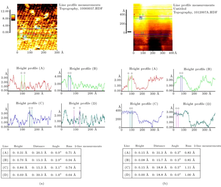
Figure 3. Atomically resolved NC-AFM images of the 0.07 ML and 0.2 ML pentacene on (2 4) InP (001) together with the images of InP terraces prior to the deposition.
pentacene on (24) InP (001), together with images of InP terraces prior to deposition are shown in Figure 3. The 3D image of the 0.07 ML pentacene on (24) InP (001) presented in Figure 4 shows the incipient formation of standing mode dendritic-like ordering of the pentacene molecules.
The identication of the pentacene molecule or-dering on the (2 4) InP (001) is made possible by the line prole measurements of the atomically resolved
Figure 4. 3-D atomically resolved image of the 0.07 ML pentacene on (2 4) InP (001).
images. The results of the line analysis of the two atomically resolved images from Figure 3 are shown in Figure 5.
On line proles B and C, taken on the level of two formed pentacene molecules, (Figure 5a), an intermolecular distance of 15.3A in agreement with the previously reported pentacene inter-planar spacing (d001 = 15:4 A) has been retrieved. On line prole
D, the distance between 3 consecutive substrate atoms (equivalent to two inter-planar spacings of the sub-strate lattice) is quite accurately found to be 38.3 A. In Figure 5b, corresponding to the 0.2 ML pentacene on (2 4) InP, line proles A and B are drawn on the level of the supposed pentacene molecules grown onto the InP. On line A, the distance between 3 consecutive pentacene molecules (equivalent to two interplanar spacings) is found to be 31.3 A, in good agreement with the reported value of d001= 15:4 A. On line B, the
inter-planar distance (15.7 A) is also found to be quite close to the reported pentacene inter-planar distance. On the contrary, from line proles C and D, on the InP substrate lattice, an accurate interplanar distance is found to be 18.8 A. Thus, the line prole measurements of atomically resolved images (Figure 5) have allowed precise identication of the interplanar spacings of both InP substrate lattice and the d001of the pentacene, and
Figure 5. Line prole measurements on atomically resolved NC-AFM images of 0.07 ML (a) and 0.2 ML (b) pentacene on (2 4) InP.
pentacene molecules in a standing growth mode in the submonolayer regime.
Case of Au on (2 4) InP
The deposition of metals onto the (2 4) InP (001) reconstructed surfaces has also been attempted. In the submonolayer regime -0.1 ML of Au- the formation of elongated well-ordered nanostructures onto InP do not occur. Instead, quasi-regular monodispersed Au nano-dots were observed (Figure 6). The reasons for this behavior, dierent from the case of Au on the InSb surface, are not yet understood, but they may reside in the mixed-dimer model commonly associated with the (2 4) InP (001) highly corrugated polar surface. In the case of (2 4) InP, it has been shown [8] that post-sputtering annealing to temperatures higher that 750 K leads to the formation of many In droplets.
compete with the o-stoichiometric surface sites due to the high mobility of the In atoms during the sputtering and metal deposition. It means that locally In enriched surface regions may act as nucleation centers for the Au atoms.
CONCLUSION
Functionalized surfaces, in the form of regular terraces, by using ion-beam sputtering of ultrasmooth semicon-ductor surfaces, have been developed. It has been shown that the formation of regular nanostructures to be used as a template for architectured nanostructures is controlled by the experimental parameters. By using non-contact atomic force microscopy with atomic res-olution, incipient formation of continuous terraces and elongated features along the direction of the sputtering beam is observed. After the 4th cycle of sputtering, the surface presents atomically at terraces separated by steps of monolayer height, oriented preferentially, along the direction of the sputtering beam. The size of the terraces ranges between few tens and hundreds of nanometers. On these functionalized surfaces, sub-monolayer metallic or molecular nanostructures have been grown and the as-formed structures were in-situ imaged by NC-AFM. In the case of pentacene grown onto (2 4) reconstructed InP (0 0 1), it has been observed that during the initial stages of growth, a uniaxial diusion channel dominates, and long pentacene molecular chains self-organize parallel to the [110] crystallographic direction on the InP surface. Atomically resolved NC-AFM images were allowed to unambiguously identify the pentacene self-organized onto the terraces by measuring interplanar distances. A standing growth mode has been proven for the pentacene molecules, if the coverage fraction is within the submonolayer regime. In the case of Au onto a (2 4) reconstructed InP (0 0 1) surface, the forma-tion of nanodots was observed. Such a growth mode can be explained by taking into account that possible In-rich regions formed during the reconstruction of the surfaces may act as nucleation sites for the metal dots formation.
ACKNOWLEDGMENT
Part of this work has been performed in the De-partment of Physics, Jagiellonian University, Krakow, Poland. Financial support from the Romanian Min-istry of Research through PN II projects 71-060 / 2007 and 12-129 / 2008 is gratefully acknowledged.
REFERENCES
1. Murray, C.B., Kagan, C.R. and Bawendi, M.G. \Self-organization of CdSe nanocrystallites into
3-dimensional quantum-dot superlattices", Science, 270(5240), pp. 1335-1338 (1995).
2. Wolf, S.A., Awschalom, D.D., Buhrman, R.A., Daughton, J.M., von Molnar, S., Roukes, M.L., Chtchelkanova, A.Y. and Treger, D.M. \Spintronics: A spin-based electronics vision for the future", Science, 294(5546), pp. 1488-1495 (2001).
3. de Mongeot, F.B., Boragno, C. and Valbusa, U. \Nanostructuring surfaces by ion erosion", in Atom-istic Aspects of Epitaxial Growth, M. Kortla, Ed., pp. 221-225, Kluwer Academic Publishers, Amsterdam, NL (2002).
4. Materials Modication by Electronic Exs, N. Itoh and A.M. Stoneham, Eds., Cambridge University Press, UK (2001).
5. Rusponi, S., Constantini, G., Boragno, C. and Val-busa, U. \Ripple wave vector rotation in anisotropic crystal sputtering", Phys. Rev. Lett., 81(13), pp. 2735-2738 (1998).
6. Rusponi, S., Constantini, G., Boragno, C. and Val-busa, U. \Scaling Laws of the Ripple Morphology on Cu(110)", Phys. Rev. Lett., 81(13), pp. 4184-4187 (1998).
7. Kolodziej, J.J., Such, B. and Szymonski, M. \Imaging of c(8 2)=(4 6) GaAs(001) surface with noncontact atomic force microscopy", Phys. Rev. B, 71(16), p. 165419 (2005).
8. Kolodziej, J.J., Such, B., Goryl, M., Krok, F., Piatkowski, P. and Szymonski, M. \Surface struc-ture investigations using noncontact atomic force mi-croscopy", Appl. Surf. Sci., 252(21), pp. 7614-7623 (2006).
9. Giessibl, F.J. \Atomic resolution of the silicon (111)-(7 7) surface by atomic force microscopy", Science, 267(5194), pp. 68-71 (1995).
10. Such, B., Kolodziej, J.J., Krok, F., Piatkowski, P. and Szymonski, M. \Non-contact atomic force microscopy studies of (2 4) InP(0 0 1) surface", Surf. Sci., 600(11), pp. 2379-2384 (2006).
11. Kolodziej, J.J., Goryl, M., Konior, J., Krok, F. and Szymonski, M. \PTCDA molecules on an InSb(001) surface studied with atomic force microscopy", Nan-otechnology, 18(13), p. 135302 (2007).
12. Killampalli, A.S., Schroeder, T.W. and Engstrom, J.R. \Nucleation of pentacene on silicon dioxide at hyperthermal energies", Appl. Phys. Lett., 87(3), p. 033110 (2005).
13. Crisan, O., Angelakeris, M., Papaioannou, E., Crisan, A.D., Flevaris, N.K., Vouroutzis, N., Pavlidou, E., Kostic, I., Sobal, N. and Giersig, M. \Magnetic nanos-tructures obtained by colloidal crystallization onto patterned substrates", J. Magn. Magn. Mater., 272-276(1), pp. e1285-e1287 (2004).
14. Crisan, O., Angelakeris, M., Nogues, M., Papaioannou, E., Flevaris, N.K., Komninou, Ph., Kehagias, Th., Sobal, N. and Giersig, M. \Correlation of structure and magnetism of Ag/Co nanoparticle arrays", J. Magn. Magn. Mater., 272-276(1), pp. e1253-e1254 (2004).
15. Crisan, O., Angelakeris, M., Simeonidis, K., Kehagias, Th., Komninou, Ph., Giersig, M. and Flevaris, N.K. \Structure eects on the magnetism of AgCo nanopar-ticles", Acta Materialia, 54(19), pp. 5251-5260 (2006). 16. Crisan, O., Le Breton, J.M. and Filoti, G. \Nanocrys-tallization of soft magnetic Finemet-type amorphous ribbons", Sensors & Actuators A, 106(1), pp. 246-250 (2003).
17. Crisan, O., Labaye, Y., Berger, L., Coey, J.M.D. and Greneche, J.M. \Exchange coupling eects in nanocrystalline alloys studied by Monte Carlo simu-lation", J. Appl. Phys., 91(10), pp. 8727-8729 (2002). 18. Seqqat, M., Nogues, M., Crisan, O., Kuncser, V., Cristea, L., Jianu, A., Filoti, G., Dormann, J.L., Sayah, D. and Godinho, M. \Magnetic properties of Fe100 xSmx thin lms and Fe80 xSmxB20 thin lms
and ribbons", J. Magn. Magn. Mater., 157-158, pp. 225-226 (1996).
19. Crisan, O., von Haeften, K., Ellis, A.M. and Binns, C. \Structure and magnetic properties of Fe/Fe oxide clusters", J. Nanopart. Res., 10(suppl.1), pp. 193-199 (2008).
20. Crisan, O., von Haeften, K., Ellis, A.M. and Binns, C. \Novel gas-stabilized iron clusters: synthesis, structure and magnetic behavior", Nanotechnology, 19(50), p. 505602 (2008).
21. Yoshikawa, G., Miyadera, T., Onoki, R., Ueno, K., Nakai, I., Entanic, S., Ikeda, S., Guo, D., Kiguchi, M., Kondoh, H., Ohta T. and Saiki, K. \In-situ measurement of molecular orientation of the pentacene ultrathin lms grown on SiO2 substrates", Surf. Sci.,
600(12), pp. 2518-2522 (2006).
22. Ruiz, R., Mayer, A.C., Malliaras, G.C., Nickel, B., Scoles, G., Kazimirov, A., Kim, H., Headrick, R.L. and Islam, Z. \Structure of pentacene thin lms", Appl. Phys. Lett., 85(21), p. 4926 (2004).
23. Pratontep, S., Brinkmann, M., Nuesch, F. and Zup-piroli, L. \Correlated growth in ultrathin pentacene
lms on silicon oxide: Eect of deposition rate", Phys. Rev. B, 69(16), p. 165201 (2004).
24. Pratontep, S., Brinkmann, M., Nuesch, F. and Zup-piroli, L. \Comparison between nucleation of pen-tacene monolayer islands on polymeric and inorganic substrates", Phys. Rev. B, 72(8), p. 08521 (2005).
BIOGRAPHY
Ovidiu Crisan is Senior Researcher and a member of the Scientic Board of the National Institute for Materials Physics, Bucharest, Romania. He obtained his Ph.D. at the Universite de Rouen, France, in 1998, with a thesis on the study of the inuence of rare earth on the structure and magnetism of nanocrystalline soft magnetic alloys. Since obtaining his Ph.D., he has worked as a Postdoctoral in various universities and research institutes in many countries. Since 2008, he holds a Senior Researcher 1st degree position at the National Institute for Materials Physics. His research interests in the larger eld of Nanostructured Materials with Advanced Functionalities are extremely broad. They range from Molecular Nanostructures onto Ion-beam Patterned/Functionalized Semiconductor Sur-faces to Self-assembled Colloidal Core-shell Nanopar-ticles for Spintronics Applications and Nanoclusters by Cluster Aggregation Techniques, or from Phase Transformations in Intermetallic Alloys to Interlayer Exchange Coupling in Thin Films and Multilayers by Inelastic Resonant Scattering. He was awarded the Diploma of Excellence in Research by the National Agency for Scientic Research, Romania, in 2000, for his work in giant magnetoresistive exchange-coupled heterogranular alloys. He was also awarded, in 2006, the \Horia Hulubei" Prize, a once-in-a-lifetime award, by the Romanian Academy, Physics Section, for out-standing results in the eld of innovative magnetic materials with high applicative potential.