AUSTRALIAN JOURNAL OF BASIC AND
APPLIED SCIENCES
ISSN:1991-8178 EISSN: 2309-8414 Journal home page: www.ajbasweb.com
Open Access Journal
Published BY AENSI Publication
© 2016 AENSI Publisher All rights reserved
This work is licensed under the Creative Commons Attribution International License (CC BY).
http://creativecommons.org/licenses/by/4.0/
To Cite This Article: M.Jayashree, I.Poonguzhali, S.Selva Agnes., An Efficient High Throughput Implementation of IDEA Encryption Algorithm using VLSI. Aust. J. Basic & Appl. Sci., 10(1): 337-344, 2016
An Efficient High Throughput Implementation of IDEA Encryption
Algorithm using VLSI
1M.Jayashree, 2I.Poonguzhali, 3S.Selva Agnes
1Department of ECE, Panimalar Institute of Technology 2Department of ECE, Panimalar Institute of Technology 3Department of ECE, Panimalar Institute of Technology
Address For Correspondence:
M.Jayashree, Department of ECE, Panimalar Institute of Technology E-mail: [email protected]
A R T I C L E I N F O A B S T R A C T Article history:
Received 10 December 2015 Accepted 28 January 2016 Available online 10 February 2016
Keywords:
IDEA, Encryption, Decryption, Throughput, pipelining, Wallace Tree Compressor.
Implementation of IDEA encryption algorithm with high throughput using Verilog HDL is described in this paper. This is achieved by optimizing the modulus multiplier and using the available temporal parallelism in IDEA algorithm. The inverse modulo (2n+1) multiplier design implemented using the power realization algorithm for Euler’s theorem results in the fast inverse modulo multiplier. For high throughput a multiplier including Wallace tree compressors and carry look-ahead adders is used in pipelined implementations. In this algorithm, the sub-keys are generated internally. The original key once fetched is retained unless a new key is used for encryption. A significant improvement in area is achieved, as additional RAM is not engaged to store the sub-keys. The algorithm is executed in parallel for eight rounds using pipelined design. A key change results in latency of only three clock cycles, and the throughput is improved significantly due to the pipelined design. This implementation achieves a throughput of 1.422 Gbps, operating at a frequency of 66.67 MHz and cell area of 1.77 mm².
INTRODUCTION
Recently, the number of individuals and organizations using wide computer networks for personal and professional activities has increased a lot. Among them, there are several applications highly sensitive to data security such as commercial exchange on the Internet and smart cards. A cryptographic algorithm is an essential part in network security. A well-known cryptographic algorithm is the Data Encryption Standard (DES), which is widely adopted in security products. However, serious considerations arise from long-term security because of the relatively short key word length of only 56bits and recently from the highly successful cryptanalysis attack. (Ms Snehal Patil, Prof.Vrunda Bhusari, 2014) There was a call for a stronger algorithm, and International Data Encryption Algorithm (IDEA) came into picture in1990. IDEA uses algebraic operations completely and it entirely avoids the use of any lookup tables or S-boxes. The strength of IDEA lies in its modulo multiplication operations. Using pipelined design, eight rounds of the algorithm are executed in parallel in a chip. The objective of this project is to reduce hardware requirements, resulting in a significant improvement in silicon area, processing speed and high throughput. For this purpose design of multiplier is very crucial. The time required for multiplication modulo (216+1) has a significant influence on the system clock frequency.
Many researchers have implemented the IDEA algorithm. Curiger et al. (1991) has implemented a chip which is the first silicon device that can be applied to on-line encryption in high-speed networking protocols like ATM. With a system clock frequency of 25 MHz, this device permits a data conversion rate of 177 Mbps. Salomao et al. (1998) has implemented a single round of IDEA on one chip, and it operates at a worst case clock frequency of 30 MHz producing a throughput of 424
Mbps. Qin et al. (MediaCrypt) has also implemented a chip whose maximum clock time period and throughput reported are 8 and 133 Mbps, respectively. The purpose of our design is to demonstrate the feasibility of hardware implementation of IDEA that is one of the most popular encryption algorithms with high throughput. The rest of the paper is organized as follows. Section 2 describes the IDEA cryptographic algorithm. Section 3 describes how IDEA is implemented in VLSI using Verilog HDL. Section 4 gives the results obtained. Finally, Section 5 concludes the paper.
2. The Idea Cryptographic Algorithm:
The block cipher IDEA was first presented by Xuejia Lai and James Massey of the Swiss Federal Institute of Technology in 1990 and was then called PES (Proposed Encryption Standard) (MediaCrypt; Lai, X. and J. Massey, 1990). In 1991 after Biham and Shamir presented their results regarding differential cryptanalysis, the authors developed an improved version of the PES algorithm to increase the security against this attack and the new algorithm was called IPES (Improved Proposed Encryption Standard) while finally in 1992 its name was changed officially to IDEA.
The IDEA is a symmetric, block oriented encryption algorithm, which operates on a 64-bit plaintext and uses a 128 bit length key. The substitution boxes and the associated “lookup tables” used in the rest block ciphers available to-date (and among them DES) have been completely dispensed with. The required confusion in this algorithm is achieved by successively using three different and “incompatible group operations on pairs of 16-bit sub-blocks and mixing them (in such a way that at no point in the encryption process the same algebraic operation is used contiguously) while the structure of the cipher was carefully chosen to provide the necessary diffusion requirement”. These three algebraic operations are the following:
• Bit-by bit XOR
• Addition of integers modulo (216+1) with inputs and outputs treated as unsigned 16-bit integers
• Multiplication of integers modulo (216+1) with inputs and outputs treated as unsigned 16-bit integers (This operation can be also viewed as IDEA’s equivalent S-box.)
All these operations operate on 16-bit sub-blocks. Their use in combination provides for a complex transformation of the input making cryptanalysis much more difficult than with an algorithm such as e.g. DES, which relies solely on the XOR function.
IDEA uses a 128 bit key which is double the key size of DES. Thus, making it highly immune to attacks. IDEA uses algebraic operations completely and it entirely avoids the use of any lookup tables or S-boxes. The strength of IDEA lies in its modulo multiplication operations.
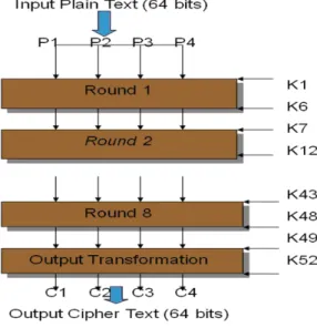
Fig. 1: Architecture of IDEA
K43 to K48. The final step consists of an Output Transformation, which uses just 4 sub-keys. The final output produced is the output produced by the Output Transformation round. (Chaudhari, A.D., S.D. Shirbahadurkar, 2013).
2.1 Key generation:
The initial 6 sub-keys K1 to K6 are generated from the original 128 bit key. Since the sub-keys consist of 16 bits each, out of the original 128 bits, the first 96 bits are used for the first round. Thus, at the end of the first round, bits97-128 of the original key are unused. This is illustrated in fig.2. In the second round, the unused 32 bits of the first round are used. To generate the rest of the sub-keys for the second round, 64 more bits are required.
Fig. 2: key generation for the 1st round
This is obtained by shifting the original key left circularly by 25 bits. Then, the modified key is now used to generate the rest of the 4 sub-keys in the same way as the first round keys were generated. The same is done for the sub-key generation for the rest of the rounds.
In each round of the 8 rounds of algorithm, the following sequences of events are performed: (Webpage:www.finecrypt.com), as shown in fig.3.
1. multiply* P1 and K1 2. add* P2 and K2 3. add* P3 and K3 4. multiply* P4 and K4
5. XOR the results of step 1 and step 3 6. XOR the results of step 2 and step 4 7. multiply* the results of step 5 with K5 8. add* the results of step 6 and step 7 9. multiply* the results of step 8 with K6 10. add* the results of step 7 and step 9 11. XOR the results of step 1 and step 9 12. XOR the results of step 3 and step 9 13. XOR the results of step 2 and step 10 14. XOR the results of step 4 and step 10
Sequence of events followed in the output transformation round:-
1.Multiply* R1 and K1
2.Add* R2 and K2
3.Add* R3 and K3
4.Multiply* R4 and K4
The outputs of the round are given in the same order to the next round. After the 8th round, the inner 2 blocks are swapped and given as input to the final transformation round (Nikos Sklavos). Finally, the four sub-blocks are attached to get the final encrypted result.
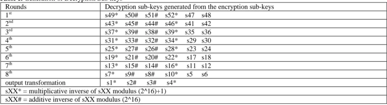
Decryption uses exactly the same sequence of operations of successive 64-bit blocks of the cipher text, but with a different set of sub keys. The same 52 key sub-blocks generated for encryption are rearranged and inverted accordingly to produce the decryption key schedule. Those that are added are replaced by their two's complement. Those that are multiplied in are replaced by their multiplicative inverse, modulo 65,537, but those used to calculate the cross-footed F-functions are not changed. Keys XORed in would not need to be changed, but there aren't any such keys in IDEA.
Decryption sub-keys required per round cannot be generated per clock cycle. This is due to the modular inversion process. Hence, for decryption, the IDEA Core will stall until all the decryption sub-keys are generated for that round. The decryption sub keys (relative to the encryption sub keys s1 to s52) are generated as shown below in table I (Webpage:www.finecrypt.com):-
Table I: Generation of Decryption Sub keys
Rounds Decryption sub-keys generated from the encryption sub-keys
1st s49* s50# s51# s52* s47 s48
2nd s43* s45# s44# s46* s41 s42
3rd s37* s39# s38# s39* s35 s36
4th s31* s33# s32# s34* s29 s30
5th s25* s27# s26# s28* s23 s24
6th s19* s21# s20# s22* s17 s18
7th s13* s15# s14# s16* s11 s12
8th s7* s9# s8# s10* s5 s6 output transformation s1* s2# s3# s4*
sXX* = multiplicative inverse of sXX modulus (2^16)+1) sXX# = additive inverse of sXX modulus (2^16)
3. The Vlsi Implementation of Idea:
The goal of this implementation is to achieve highest possible throughput. For this reason fast inverse modulo multiplier, carry look ahead adder and Wallace tree compressors has been used, these are explained later in the paper. In this implementation, the 128-bit key is latched into the chip on the first clock signal depending on the key latch signal (Thaduri, M., et al., 2004). The designing has been done in such a way so that for the next consecutive clock triggers, eight new sub-keys are generated and four more are generated at the next clock trigger. Now, using these encryption sub-keys, decryption sub-keys are generated. Decryption sub-keys required per round cannot be generated per clock cycle. This is due to the modular inversion process. Hence, for decryption, the IDEA Core will stall until all the decryption sub-keys are generated for that round.
For parallel, synchronous implementation of IDEA algorithm, each round is implemented in a single clock cycle. The designing has been done in such a way that, as the first eight sub-keys are generated, the intermediate results are passed to the first round of IDEA algorithm. Thus, at the next clock trigger the second eight sub-keys are generated as well as the first round of IDEA algorithm is also executed and so on. The resulting ciphertext is then given as input to the decryption part. The steps involved in decryption are exactly similar to the encryption part, except that the input is the ciphertext and the decryption sub-keys are used instead of encryption sub-keys.
3.1 Fast Inverse Modulo Multiplier:
The design of inverse modulo (216+1) multiplier is done using a novel realization of the power algorithm for Euler’s theorem, which results in the fast inverse modulo multiplier. (Dr.Nabil Hamdy) Euler's totient function is written as Ø(n). For prime number p: Ø (p) = p-1. Thus to get the multiplicative inverse of ‘K’ such that (K) is relatively prime to ( n ):
(K‾¹) mod n =K (Ø (n)-l) mod n.
For prime number, n = (216 + 1) = 65537, Ø (216 + 1) = 65536 and
(K ‾¹) mod (216 + 1) = K(Ø(2^16+1)-1)mod(216+1) = K(65535)mod (216 +1).
Using the fast Power Algorithm, which states that:
The fast inverse modulo multiplier calculates the inverse keys in only 30 clocks using Euler's Theorem besides the power algorithm. The inverse multiplicative key can be calculated through squaring the output from the modulo multiplication operation then storing this output to use it again. This is done until the modulo multiplication circuit generates K(32768)mod(216 +1) which is equal to K15. Then K15 is modulo multiplied with the other stored fifteen values. Through the calculation of the following equation the inverse multiplicative key is generated in 30 clocks. (((K * K15 mod (216+ 1)) * K1 mod (216+1)) * K2 mod (216 +1)) * ... and so on till multiply the output with X14 mod (216+1). The fast inverse modulo multiplier circuit can generate the 18 decryption sub keys in only 18x30 clocks compared to 18x65535 clocks using Euler's Theorem only.
3.2 Multiplier Unit:
Computers have always multiplied slowly regardless of whether a software subroutine or a hardware/software approach was used. (Webpage:www.finecrypt.com) The multiplier in this design uses very little software, as a result multiplication takes place at a very a fast speed. It is composed of three blocks. The first is a partial product generator. The second is the Wallace tree section which adds all of the partial products simultaneously to produce two numbers. The third is the carry look ahead adder that adds the two numbers, obtained from the Wallace tree section. After generating the partial products, Wallace 3:2 compressors are used to quickly generate the final two vectors, which are added using a carry look ahead adder. Then the final modulus of the 32-bit result is found.
3.2.1 Partial Product Generation:
Using Carry-Save Adder (i.e. Full adders and AND gates) the partial products as illustrated above are generated as shown in the Fig.4
Fig. 4: Partial Product Generation using Carry-Save adders
3.2.2 Partial Product Addition Using Wallace tree compressors:
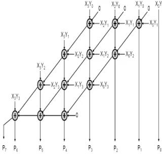
To improve the speed of multiplication, Wallace tree compressors are used to add the partial products. A Wallace tree is a full adder tree structured specially for a quick addition of the partial products. A k-input Wallace tree is a bit-slice summing circuit, which produces the sum of k-bit input slices. This is shown in fig.5.
Modulo Multiplier:
Earlier, two methods were proposed to implement modulo (2n +1 ) multiplier- 1) Division by (subtract and shift) or
2) Systolic Array
The division technique is based on subtracting the modulo number from the multiplication result until the subtraction result is less than the modulo number. The systolic array is based on Montgomery Algorithm. The analysis of the hardware implementation for the two techniques shows that, the first technique is very slow and the result comes after several times of subtraction controlled by a comparator while the second technique is very hard to implement beside it needs huge number of logic gates. The used mathematical formula to implement the modulo (2n+1) multiplier is as follows (Dr.Nabil Hamdy):
{(a*b)mod2n-(a*b)/2n if{(a*b)mod2n>=(a*b)/2n}
(a*b)mod(2n+1)= {(a*b)mod2n-(a*b)/2n+2n+1
if {(a*b)mod2n<(a*b)/2n}} The implementation of this modulo multiplier is very fast and very efficient compared with the other two
techniques.
3.2.3 Carry-look ahead adder:
When two n-bit numbers are added, the total time for computing the final n-bit sum is 2(n-1)+3 gate delays, when n=16, there will 33 gate delays. The bottle neck for ripple carry addition is the calculation of c[i], which takes linear time proportional to ‘n’, the number of bits in the adder. To improve, we define
Generate function: g[i] = x[i] & y[i] Propagate function: p[i] = x[i] | y[i] Carry: c [i+1] =
g[i]+p[i]g[i-1]+…….+p[i]p[i-1]….p[0]c[0]
But, if n>=16 this even may take enough time to compute the output. To avoid this block carry look ahead adder is used, given in fig.6
Fig. 6: Carry look ahead adder
Simulation And Synthesis Results:
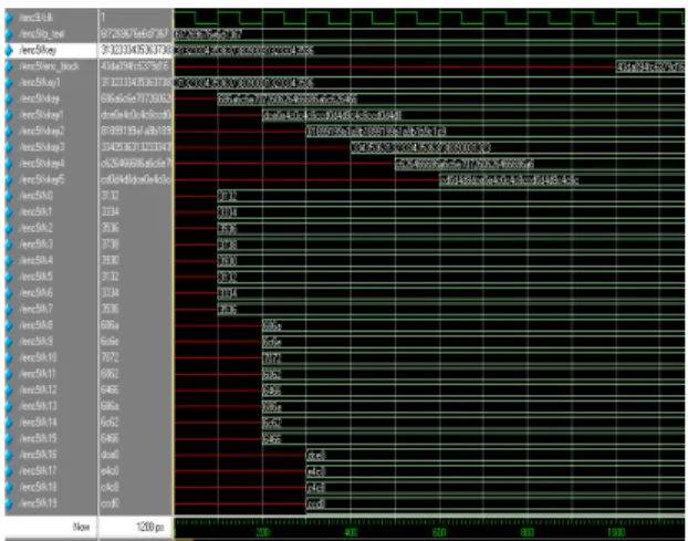
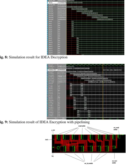
The codes were written in Verilog HDL language, simulated in Xilinx 9.1i/Modelsim 6.2c and synthesized in Encounter(r) RTL Compiler. The Fig 7. shows the plaintext and the key as input and ciphertext as the output (Irwin Yoon's ECE575). The Fig 8. shows the ciphertext as the input and the plaintext back as output. The Fig 9. shows the plaintext and the key as input and ciphertext as the output for Encryption with pipelining. The complete architecture of the chip is given in Fig 10.
Fig. 8: Simulation result for IDEA Decryption
Fig. 9: Simulation result of IDEA Encryption with pipelining
Fig. 10: RTL Schematic of IDEA Algorithm
Table II: Performance comparison
Reference Clock Frequency(MHz) Throughput (Mbps) Area
(mm²)
Existing [1] 10 700 1.95
Proposed 66.67 1422 1.77
The Table II shows the performance comparison of Synthesis Report obtained using Encounter(r) RTL Compiler. From the table it is clear that the throughput of proposed work is twice that of the existing one.
Conclusion:
REFERENCES
Bhasker, J., Verilog VHDL Synthesis, A Practical Primer, Star Galaxy Publishing, 1998. Lucent Technologies.
Chaudhari, A.D., S.D. Shirbahadurkar, 2013. “VHDL Implementation of IDEA Architectures” International Journal of Innovative Technology and Exploring Engineering (IJITEE) ISSN: 2278-3075, 3: 1.
Curiger, A., H. Bonnenberg, 1991. H.kaeslin, Regular VLSI architectures for multiplication modulo (2n + 1), IEEE J, Solid-State Circuits, pp: 990-994.
Dr.Nabil Hamdy, Dr. Khaled Shehata, Dr.Salah Elagooz, Eng. Mohamed Helmy, ”Design and
Implementation of Fast Inverse Modulo (216+1) Multiplier Used in IDEA Algorithm Key Schedule on FPGA”.
Irwin Yoon's ECE575 Project - IDEA Algorithm http://islab.oregonstate.edu/koc/ece575/03Project /Yoon/ Lai, X. and J. Massey, 1990. “A proposal for a new block encryption standard,” Proceedings, Eurocrypt, 90.
MediaCrypt: IDEA Technical Description. http://web.engr.oregonstate.edu/~laige/ece575/
IDEA%20Technical%20Description_0503.pdf
Ms Snehal Patil, Prof.Vrunda Bhusari, 2014. “An Enhancement In International Data Encryption Algorithm For Increasing Security”, International Journal of Application on Innovation in Engineering & Management (IJAIEM), ISSN 2319 – 4847, 3: 8.
Nikos Sklavos, Alexandros Papakonstantinou, Spyros Theoharis and Odysseas Koufopavlou, “ Low-power Implementation of an Encryption/Decryption System with Asynchronous Techniques”.
Salomao, S., V. Alves, E. Filho, 1998. HiPCrypto: a high-performance VLSI cryptographic chip, IEEE Int. ASIC Conf. pp: 7-11.
Thaduri, M., S.-M. Yoo*, R. Gaede, 2004. “An efficient implementation of IDEA encryption algorithm using VHDL”, ©2004 Elsevier.