D
2.5-V Virtual Ground for 5-V/GND Analog
Systems
D
High Output-Current Capability
Sink or Source . . . 20 mA Typ
D
Micropower Operation . . . 170
µ
A Typ
D
Excellent Regulation Characteristics
− Output Regulation
−45
µ
V Typ at I
O= 0 to − 10 mA
+15
µ
V Typ at I
O= 0 to + 10 mA
− Input Regulation = 1.5
µ
V/V Typ
D
Low-Impedance Output . . . 0.0075
Ω
Typ
D
Macromodel Included
description
In signal-conditioning applications using a single
power source, a reference voltage is required for
termination of all signal grounds. To accomplish
this, engineers have typically used solutions
consisting of resistors, capacitors, operational
amplifiers, and voltage references. Texas
Instru-ments has eliminated all of those components
with one easy-to-use 3-terminal device. That
device is the TLE2425 precision virtual ground.
Use of the TLE2425 over other typical circuit
solutions gives the designer increased dynamic
signal range, improved signal-to-noise ratio,
lower distortion, improved signal accuracy, and
easier interfacing to ADCs and DACs. These
benefits are the result of combining a precision
micropower voltage reference and a
high-perfor-mance precision operational amplifier in a single
silicon chip. It is the precision and performance of
these two circuit functions together that yield such
dramatic system-level performance.
The TLE2425 improves input regulation as well as output regulation and, in addition, reduces output impedance
and power dissipation in a majority of virtual-ground-generation circuits. Both input regulation and load
regulation exceed 12 bits of accuracy on a single 5-V system. Signal-conditioning front ends of data acquisition
systems that push 12 bits and beyond can use the TLE2425 to eliminate a major source of system error.
AVAILABLE OPTIONS TA SMALL OUTLINE(D) PLASTIC TO-226AA (LP) 0°C to 70°C TLE2425CD TLE2425CD − 40°C to 85°C TLE2425ID TLE2425ID − 55°C to 125°C TLE2425MD — † The D package is available taped and reeled. Add R suffix to
the device type (e.g., TLE2425CDR).
Please be aware that an important notice concerning availability, standard warranty, and use in critical applications of Texas Instruments semiconductor products and disclaimers thereto appears at the end of this data sheet.
V) − Output V oltage Change − µ V 80 − 20 0 20 60 40 − 40 − 60 − 80 − 100 10 8 − 2 0 2 4 6 − 4 − 6 − 8 − 10 100 OUTPUT REGULATION IO − Output Current − mA VI = 5 V TA = − 55°C TA = 25°C TA = 125°C ∆ VO TA = − 40°C TA = 125°C TA = − 55°C TA = 0°C TA = 25°C
1 2 3 4 8 7 6 5 OUT COMMON IN NC NC NC NC NC D, OR JG PACKAGE (TOP VIEW) NC − No internal connection OUT IN COMMON LP PACKAGE (TOP VIEW)
absolute maximum ratings over operating free-air temperature range (unless otherwise noted)
†
Continuous input voltage, V
I. . .
40 V
Output current, I
O. . .
±
80 mA
Duration of short-circuit current at (or below) 25
°
C (see Note 1)
. . .
unlimited
Continuous total power dissipation
. . .
See Dissipation Rating Table
Operating free-air temperature range, T
A: C-suffix 0
. . .
°
C to 70
°
C
I-suffix −40
. . .
°
C to 85
°
C
M-suffix −55
. . .
°
C to 125
°
C
Storage temperature range, T
stg−65
. . .
°
C to 150
°
C
Lead temperature 1,6 mm (1/16 inch) from case for 10 seconds: D package
. . .
260
°
C
Lead temperature 1,6 mm (1/16 inch) from case for 60 seconds: JG or LP package
. . .
300
°
C
† Stresses beyond those listed under “absolute maximum ratings” may cause permanent damage to the device. These are stress ratings only, and functional operation of the device at these or any other conditions beyond those indicated under “recommended operating conditions” is not implied. Exposure to absolute-maximum-rated conditions for extended periods may affect device reliability.
NOTE 1: The output may be shorted to either supply. Temperature and/or supply voltages must be limited to ensure that the maximum dissipation rating is not exceeded.
DISSIPATION RATING TABLE
PACKAGE TA ≤ 25°C DERATING FACTOR TA = 70°C TA = 85°C TA = 125°C PACKAGE TA ≤ 25 C POWER RATING DERATING FACTOR ABOVE TA = 25°C TA = 70 C POWER RATING TA = 85 C POWER RATING TA = 125 C POWER RATING D 725 mV 5.8 mW/°C 464 mW 377 mW 145 mW JG 1050 mV 8.4 mW/°C 672 mW 546 mW 210 mW LP 775 mV 6.2 mW/°C 496 mW 403 mW 155 mW
recommended operating conditions
C-SUFFIX I-SUFFIX M-SUFFIX
UNIT
MIN MAX MIN MAX MIN MAX UNIT
Input voltage, VI 4 40 4 40 4 40 V
electrical characteristics at specified free-air temperature, V
I
= 5 V, I
O
= 0 (unless otherwise noted)
PARAMETER TEST CONDITIONS TA† TLE2425C UNIT
PARAMETER TEST CONDITIONS TA†
MIN TYP MAX UNIT
Output voltage 25°C 2.48 2.5 2.52 V
Output voltage
Full range 2.47 2.53 V
Temperature coefficient of output voltage 25°C 20 ppm/°C
Bias current IO = 0 25°C 170 250 A
Bias current IO = 0
Full range 250 µA
VI = 4.5 V to 5.5 V 25°C 1.5 20 V
Input voltage regulation
VI = 4.5 V to 5.5 V Full range 25 µV
Input voltage regulation
VI = 4 V to 40 V
25°C 1.5 20
V/V
VI = 4 V to 40 V Full range 25 µV/V
Ripple rejection f = 120 Hz, ∆VI(PP) = 1 V 25°C 80 dB
IO = 0 to − 10 mA 25°C − 160 − 45 160
Output voltage regulation (source current)‡ IO = 0 to − 10 mA Full range − 250 250 µV Output voltage regulation (source current)‡
IO = 0 to − 20 mA 25°C − 450 − 150 450
µV
IO = 0 to 10 mA
25°C − 160 15 160
Output voltage regulation (sink current)‡ IO = 0 to 10 mA Full range − 250 250 µV Output voltage regulation (sink current)‡
IO = 0 to 20 mA 25°C − 235 65 235
µV
Long-term drift of output voltage ∆t = 1000 h, Noncumulative 25°C 15 ppm
Output impedance 25°C 7.5 22.5 mΩ
Short-circuit output current (sink current) VO = 5 V
25°C 30 55 mA
Short-circuit output current (source current) VO = 0 25°C − 30 − 50 mA
Output noise voltage, rms f = 10 Hz to 10 kHz 25°C 100 µV
VO to 0.1%, CL = 0 110
Output voltage response to output current step
VO to 0.1%,
IO = ±10 mA CL = 100 pF
25°C
115
s Output voltage response to output current step
VO to 0.01%, CL = 0 25°C 180 µs
VO to 0.01%,
IO = ±10 mA CL = 100 pF 180
Output voltage response to input voltage step VI = 4.5 to 5.5 V, VO to 0.1% 25°C 12 s Output voltage response to input voltage step
VI = 4.5 to 5.5 V, VO to 0.01% 25°C 30 µs
Output voltage turn-on response VI = 0 to 5 V, VO to 0.1% 25°C
125
s Output voltage turn-on response
VI = 0 to 5 V, VO to 0.01% 25°C 210 µs
† Full range is 0°C to 70°C.
electrical characteristics at specified free-air temperature, V
I
= 5 V, I
O
= 0 (unless otherwise noted)
PARAMETER TEST CONDITIONS TA† TLE2425I UNIT
PARAMETER TEST CONDITIONS TA†
MIN TYP MAX UNIT
Output voltage 25°C 2.48 2.5 2.52 V
Output voltage
Full range 2.47 2.53 V
Temperature coefficient of output voltage 25°C 20 ppm/°C
Bias current IO = 0 25°C 170 250 A
Bias current IO = 0
Full range 250 µA
VI = 4.5 V to 5.5 V 25°C 1.5 20 V
Input voltage regulation
VI = 4.5 V to 5.5 V Full range 75 µV
Input voltage regulation
VI = 4 V to 40 V
25°C 1.5 20
V/V
VI = 4 V to 40 V Full range 75 µV/V
Ripple rejection f = 120 Hz, ∆VI(PP) = 1 V 25°C 80 dB
IO = 0 to − 10 mA 25°C − 160 − 45 160
Output voltage regulation (source current)‡ IO = 0 to − 10 mA Full range − 250 250 µV Output voltage regulation (source current)‡
IO = 0 to − 20 mA 25°C − 450 − 150 450
µV
IO = 0 to 8 mA
25°C − 160 15 160
Output voltage regulation (sink current)‡ IO = 0 to 8 mA Full range − 250 250 µV Output voltage regulation (sink current)‡
IO = 0 to 20 mA 25°C − 235 65 235
µV
Long-term drift of output voltage ∆t = 1000 h, Noncumulative 25°C 15 ppm
Output impedance 25°C 7.5 22.5 mΩ
Short-circuit output current (sink current) VO = 5 V
25°C 30 55 mA
Short-circuit output current (source current) VO = 0 25°C − 30 − 50 mA
Output noise voltage, rms f = 10 Hz to 10 kHz 25°C 100 µV
VO to 0.1%, CL = 0 110
Output voltage response to output current step
VO to 0.1%,
IO = ±10 mA CL = 100 pF
25°C
115
s Output voltage response to output current step
VO to 0.01%, CL = 0 25°C 180 µs
VO to 0.01%,
IO = ±10 mA CL = 100 pF 180
Output voltage response to input voltage step VI = 4.5 to 5.5 V, VO to 0.1% 25°C 12 s Output voltage response to input voltage step
VI = 4.5 to 5.5 V, VO to 0.01% 25°C 30 µs
Output voltage turn-on response VI = 0 to 5 V, VO to 0.1% 25°C
125
s Output voltage turn-on response
VI = 0 to 5 V, VO to 0.01% 25°C 210 µs
† Full range is − 40°C to 85°C.
electrical characteristics at specified free-air temperature, V
I
= 5 V, I
O
= 0 (unless otherwise noted)
PARAMETER TEST CONDITIONS TA† TLE2425M UNIT
PARAMETER TEST CONDITIONS TA†
MIN TYP MAX UNIT
Output voltage 25°C 2.48 2.5 2.52 V
Output voltage
Full range 2.47 2.53 V
Temperature coefficient of output voltage 25°C 20 ppm/°C
Bias current IO = 0 25°C 170 250 A
Bias current IO = 0
Full range 250 µA
VI = 4.5 V to 5.5 V 25°C 1.5 20 V
Input voltage regulation
VI = 4.5 V to 5.5 V Full range 100 µV
Input voltage regulation
VI = 4.5 V to 40 V
25°C 1.5 20
V/V
VI = 4.5 V to 40 V Full range 100 µV/V
Ripple rejection f = 120 Hz, ∆VI(PP) = 1 V 25°C 80 dB
IO = 0 to − 10 mA 25°C − 160 − 45 160
Output voltage regulation (source current)‡ IO = 0 to − 10 mA Full range − 250 250 µV Output voltage regulation (source current)‡
IO = 0 to − 20 mA 25°C − 450 − 150 450
µV
IO = 0 to 3 mA
25°C − 160 15 160
Output voltage regulation (sink current)‡ IO = 0 to 3 mA Full range − 250 250 µV Output voltage regulation (sink current)‡
IO = 0 to 20 mA 25°C − 235 65 235
µV
Long-term drift of output voltage ∆t = 1000 h, Noncumulative 25°C 15 ppm
Output impedance 25°C 7.5 22.5 mΩ
Short-circuit output current (sink current) VO = 5 V
25°C 30 55 mA
Short-circuit output current (source current) VO = 0 25°C − 30 − 50 mA
Output noise voltage, rms f = 10 Hz to 10 kHz 25°C 100 µV
VO to 0.1%, CL = 0 110
Output voltage response to output current step
VO to 0.1%,
IO = ±10 mA CL = 100 pF
25°C
115
s Output voltage response to output current step
VO to 0.01%, CL = 0 25°C 180 µs
VO to 0.01%,
IO = ±10 mA CL = 100 pF 180
Output voltage response to input voltage step VI = 4.5 to 5.5 V, VO to 0.1% 25°C 12 s Output voltage response to input voltage step
VI = 4.5 to 5.5 V, VO to 0.01% 25°C 30 µs
Output voltage turn-on response VI = 0 to 5 V, VO to 0.1% 25°C 125 µs
Output voltage turn-on response
VI = 0 to 5 V, VO to 0.01% 25°C 210 µs
† Full range is − 55°C to 125°C.
TYPICAL CHARACTERISTICS
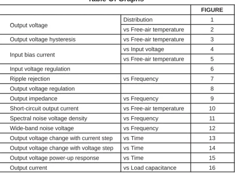
Table Of Graphs
FIGURE
Output voltage Distribution 1
Output voltage
vs Free-air temperature 2 Output voltage hysteresis vs Free-air temperature 3 Input bias current
vs Input voltage 4
Input bias current
vs Free-air temperature 5
Input voltage regulation 6
Ripple rejection vs Frequency 7
Output voltage regulation 8
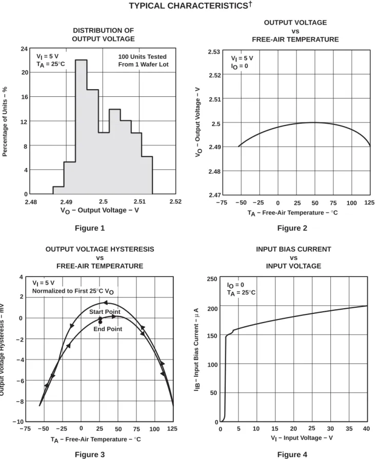
Output impedance vs Frequency 9
Short-circuit output current vs Free-air temperature 10
Spectral noise voltage density vs Frequency 11
Wide-band noise voltage vs Frequency 12
Output voltage change with current step vs Time 13 Output voltage change with voltage step vs Time 14
Output voltage power-up response vs Time 15
TYPICAL CHARACTERISTICS
†
2.48 2.49 2.5 2.51 2.52 2.47 2.53 25 50 75 100 125 0 − 25 − 50 − 75 OUTPUT VOLTAGE vs FREE-AIR TEMPERATURE 24 12 0 2.48 2.49 2.5 2.51 2.52 DISTRIBUTION OF OUTPUT VOLTAGE Percentage of Units − % VO − Output Voltage − V V) − Output V oltage − V VO TA − Free-Air Temperature − °C 20 16 8 4 VI = 5 V TA = 25°C 100 Units TestedFrom 1 Wafer Lot VI = 5 VIO = 0
Figure 1
Figure 2
200 50 0 250 150 100 5 0 10 15 20 25 30 35 40INPUT BIAS CURRENT vs
INPUT VOLTAGE OUTPUT VOLTAGE HYSTERESIS
vs FREE-AIR TEMPERATURE 2 4 0 − 2 − 4 − 6 − 10 − 8 25 50 75 100 125 0 − 25 − 50 − 75 TA − Free-Air Temperature − °C Output V oltage Hysteresis − mV VI − Input Voltage − V End Point Start Point Normalized to First 25°C VO VI = 5 V IO = 0 TA = 25°C
IIB − Input Bias Current − I IB
A
µ
Figure 3
Figure 4
TYPICAL CHARACTERISTICS
†
40 20 30 10 0 40 20 80 60 − 20 0 IO = 0 TA = 25°CINPUT VOLTAGE REGULATION
25 50 75 100 125 0 − 25 − 50 − 75 150 152 154 156 158 160 162 164 166 168 170 172
INPUT BIAS CURRENT vs FREE-AIR TEMPERATURE V) − Output V oltage Change − VI − Input Voltage − V TA − Free-Air Temperature − °C VO ∆ µ V VI = 5 V IO = 0
IIB − Input Bias Current − I IB
A µ
Figure 5
Figure 6
1 k 10 k 100 k 1 M 100 10 50 90 80 60 40 70 30 20 10 RIPPLE REJECTION vs FREQUENCY Ripple Rejection − dB f − Frequency − Hz V) − Output V oltage Change − µ V 80 − 20 0 20 60 40 − 40 − 60 − 80 − 100 10 8 − 2 0 2 4 6 − 4 − 6 − 8 − 10 100OUTPUT VOLTAGE REGULATION
IO − Output Current − mA VI = 5 V TA = 125°C ∆ VO TA = 125°C TA = − 55°C TA = 0°C TA = 25°C TA = − 40°C TA = − 55°C TA = 25°C VI = 5 V ∆VI(PP) = 1 V IO = 0 TA = 25°C
Figure 7
Figure 8
TYPICAL CHARACTERISTICS
56 54 52 50 48 46 44 42 40 25 50 75 100 125 0 − 25 − 50 − 75SHORT-CIRCUIT OUTPUT CURRENT vs
FREE-AIR TEMPERATURE
IOS − Short-Circuit Output Current − mAI OS
TA − Free-Air Temperature − °C IOS Output Sink, VO = 5 V −IOS Output Source, VO = 0 VI = 5 V 0.1 0.01 0.001 1 k 10 k 100 k 1 M 100 100 10 10 1 OUTPUT IMPEDANCE vs FREQUENCY f − Frequency − Hz − Output Impedance − Ω zo VI = 5 V TA = 25°C IO = 0 IO = − 10 mA IO = 10 mA
Figure 9
Figure 10
100 k WIDE-BAND NOISE VOLTAGEvs FREQUENCY f − Frequency − Hz VI = 5 V TA = 25°C 1 Hz to Frequency Indicated 1 Pole Low Pass
2 Pole Low Pass 80 60 40 70 30 20 10 50 0 10 100 1 k 10 k 10 100 1 k 10 k 100 k 1400
SPECTRAL NOISE VOLTAGE DENSITY vs FREQUENCY f − Frequency − Hz 1200 1000 800 600 400 200 0 1 VI = 5 V TA = 25°C W ide-Band Noise V oltage − V rms µ V − Spectral Noise V oltage Density − Vn nV/ Hz
Figure 11
Figure 12
TYPICAL CHARACTERISTICS
OUTPUT VOLTAGE RESPONSE TO INPUT VOLTAGE STEP
vs TIME − Change In Output V oltage − mV ∆ VO t − Time s 500 − 500 4 0 3 2 1 − 1 − 2 − 3 − 4 0 50 100 150 200 IO = 0 CL = 100 pF TA = 25°C VO Response VI = 5.5 V VI Step VI = 4.5 V 0.1 % 0.01 % 0.1 % VI = 4.5 V 300 450 600 750 900 1050 − 1.5 V 3 2 1 − 1 − 2 − 3 − 4 4 0 1.5 V 150 0
OUTPUT VOLTAGE RESPONSE TO OUTPUT CURRENT STEP
vs TIME − Change In Output V oltage − mV ∆ VO t − Time − s 0.1 % 0.1 % 0.01 % 0.01 % VI = 5 V CL = 100 pF TA = 25°C VO Response 10 mA IO Step 0 − 10 mA
Figure 13
Figure 14
10 − 6 − 20 5 0 − 10 − 15 − 5 20 10 15 STABILITY RANGE OUTPUT CURRENT vs LOAD CAPACITANCE I O − Output Current − mA CL− Load Capacitance − F VI = 5 V TA = 25°C Unstable Stable 10 − 5 10 − 4 10 −3 10 −2 10 −1 10 0 10 1 10 2 OUTPUT VOLTAGE POWER-UP RESPONSEvs TIME V) − Output V o ltage − V VO t − Time s IO = 0 CL = 100 pF TA = 25°C 0.1 %
Input Voltage Step
Output Voltage Response 3 2 1 0 5 0 0 10 20 130
Figure 15
Figure 16
macromodel information
* TLE2425 OPERATIONAL AMPLIFIER “MACROMODEL” SUBCIRCUIT * CREATED USING PARTS RELEASE 4.03 ON 08/21/90 AT 13:51 * REV (N/A) SUPPLY VOLTAGE: 5 V
* CONNECTIONS: INPUT * | COMMON * | | OUTPUT * | | | .SUBCKT TLE2425 3 4 5 * * OPAMP SECTION C1 11 12 21.66E − 12 C2 6 7 30.00E − 12 C3 87 0 10.64E − 9 CPSR 85 86 15.9E − 9 DCM+ 81 82 DX DCM− 83 81 DX DC 5 53 DX DE 54 5 DX DLN 92 90 DX DLP 90 91 DX DP 4 3 DX ECMR 84 99 (2,99) 1 EGND 99 0 POLY(2) (3,0) (4,0) 0 .5 .5 EPSR 85 0 POLY(1) (3,4) −16.22E−6 3.24E−6 ENSE 89 2 POLY(1) (88,0) 120E−6 1
FB 7 99 POLY(6) VB VC VE VLP VLN VPSR O 74.8E6 −10E6 10E6 10E6 + −10E6 74E6 GA 6 0 11 12 320.4E−6 GCM 0 6 10 99 1.013E−9 GPSR 85 86 (85,86) 100E−6 GRC1 4 11 (4,11) 3.204E−4 GRC2 4 12 (4,12) 3.204E−4 GRE1 13 10 (13,10) 1.038E−3 GRE2 14 10 (14,10) 1.038E−3 HLIM 90 0 VLIM 1K
HCMR 80 1 POLY(2) VCM+ VCM− 0 1E2 1E2 IRP 3 4 146E−6 IEE 3 10 DC 24.05E−6 IIO 2 0 .2E−9 I1 88 0 1E−21 Q1 11 89 13 QX Q2 12 80 14 QX R2 6 9 100.0E3 RCM 84 81 1K REE 10 99 8.316E6 RN1 87 0 2.55E8 RN2 87 88 11.67E3
macromodel information (continued)
RO1 8 5 63 RO2 7 99 62 VCM+ 82 99 1.0 VCM− 83 99 −2.3 VB 9 0 DC 0 VC 3 53 DC 1.400 VE 54 4 DC 1.400 VLIM 7 8 DC 0 VLP 91 0 DC 30 VLN 0 92 DC 30 VPSR 0 86 DC 0 RFB 5 2 1K RIN 30 1 1K RCOM 34 4 .1 *REGULATOR SECTION RG1 30 0 20MEG RG2 30 31 .2 RG3 31 35 400K RG4 35 34 411K RG5 31 36 25MEGHREG 31 32 POLY(2) VPSET VNSET 0 1E2 1E2 VREG 32 33 DC 0V
EREG 33 34 POLY(1) (36,34) 1.23 1 VADJ 36 34 1.27V
HPSET 37 0 VREG 1.030E3 VPSET 38 0 DC 20V
HNSET 39 0 VREG 6.11E5 VNSET 40 0 DC −20V DSUB 4 34 DX DPOS 37 38 DX DNNEG 40 39 DX .MODEL DX D(IS=800.0E−18) .MODEL QX PNP(IS=800.0E−18 BF=480) .ENDS
www.ti.com 11-Mar-2015
PACKAGING INFORMATION
Orderable Device Status (1)
Package Type Package Drawing Pins Package Qty Eco Plan (2) Lead/Ball Finish (6) MSL Peak Temp (3)
Op Temp (°C) Device Marking (4/5)
Samples
5962-9555601Q2A OBSOLETE LCCC FK 20 TBD Call TI Call TI -55 to 125
5962-9555601QPA OBSOLETE CDIP JG 8 TBD Call TI Call TI -55 to 125
TLE2425CD ACTIVE SOIC D 8 75 Green (RoHS
& no Sb/Br)
CU NIPDAU Level-1-260C-UNLIM 2425C
TLE2425CDG4 ACTIVE SOIC D 8 75 Green (RoHS
& no Sb/Br)
CU NIPDAU Level-1-260C-UNLIM 2425C
TLE2425CDR ACTIVE SOIC D 8 2500 Green (RoHS
& no Sb/Br)
CU NIPDAU Level-1-260C-UNLIM 2425C
TLE2425CDRG4 ACTIVE SOIC D 8 2500 Green (RoHS
& no Sb/Br)
CU NIPDAU Level-1-260C-UNLIM 2425C
TLE2425CLP ACTIVE TO-92 LP 3 1000 Pb-Free
(RoHS)
CU SN N / A for Pkg Type 2425C
TLE2425CLPR OBSOLETE TO-92 LP 3 TBD Call TI Call TI
TLE2425CPS ACTIVE SO PS 8 80 Green (RoHS
& no Sb/Br)
CU NIPDAU Level-1-260C-UNLIM Q2425
TLE2425CPSR ACTIVE SO PS 8 2000 Green (RoHS
& no Sb/Br)
CU NIPDAU Level-1-260C-UNLIM Q2425
TLE2425ID ACTIVE SOIC D 8 75 Green (RoHS
& no Sb/Br)
CU NIPDAU Level-1-260C-UNLIM 2425I
TLE2425IDG4 ACTIVE SOIC D 8 75 Green (RoHS
& no Sb/Br)
CU NIPDAU Level-1-260C-UNLIM 2425I
TLE2425IDR ACTIVE SOIC D 8 2500 Green (RoHS
& no Sb/Br)
CU NIPDAU Level-1-260C-UNLIM 2425I
TLE2425IDRG4 ACTIVE SOIC D 8 2500 Green (RoHS
& no Sb/Br)
CU NIPDAU Level-1-260C-UNLIM 2425I
TLE2425ILP ACTIVE TO-92 LP 3 1000 Pb-Free
(RoHS)
CU SN N / A for Pkg Type 2425I
TLE2425ILPE3 ACTIVE TO-92 LP 3 1000 Pb-Free
(RoHS)
CU SN N / A for Pkg Type 2425I
TLE2425MD ACTIVE SOIC D 8 75 Green (RoHS
& no Sb/Br)
www.ti.com 11-Mar-2015
Orderable Device Status (1)
Package Type Package Drawing Pins Package Qty Eco Plan (2) Lead/Ball Finish (6) MSL Peak Temp (3)
Op Temp (°C) Device Marking (4/5)
Samples
TLE2425MDRG4 ACTIVE SOIC D 8 2500 Green (RoHS
& no Sb/Br)
CU NIPDAU Level-1-260C-UNLIM -55 to 125 2425M
TLE2425MFKB OBSOLETE LCCC FK 20 TBD Call TI Call TI -55 to 125
TLE2425MJG OBSOLETE CDIP JG 8 TBD Call TI Call TI -55 to 125
TLE2425MJGB OBSOLETE CDIP JG 8 TBD Call TI Call TI -55 to 125
TLE2425MLP OBSOLETE TO-92 LP 3 TBD Call TI Call TI -55 to 125
(1)
The marketing status values are defined as follows: ACTIVE: Product device recommended for new designs.
LIFEBUY: TI has announced that the device will be discontinued, and a lifetime-buy period is in effect.
NRND: Not recommended for new designs. Device is in production to support existing customers, but TI does not recommend using this part in a new design. PREVIEW: Device has been announced but is not in production. Samples may or may not be available.
OBSOLETE: TI has discontinued the production of the device. (2)
Eco Plan - The planned eco-friendly classification: Pb-Free (RoHS), Pb-Free (RoHS Exempt), or Green (RoHS & no Sb/Br) - please check http://www.ti.com/productcontent for the latest availability information and additional product content details.
TBD: The Pb-Free/Green conversion plan has not been defined.
Pb-Free (RoHS): TI's terms "Lead-Free" or "Pb-Free" mean semiconductor products that are compatible with the current RoHS requirements for all 6 substances, including the requirement that lead not exceed 0.1% by weight in homogeneous materials. Where designed to be soldered at high temperatures, TI Pb-Free products are suitable for use in specified lead-free processes. Pb-Free (RoHS Exempt): This component has a RoHS exemption for either 1) lead-based flip-chip solder bumps used between the die and package, or 2) lead-based die adhesive used between the die and leadframe. The component is otherwise considered Pb-Free (RoHS compatible) as defined above.
Green (RoHS & no Sb/Br): TI defines "Green" to mean Pb-Free (RoHS compatible), and free of Bromine (Br) and Antimony (Sb) based flame retardants (Br or Sb do not exceed 0.1% by weight in homogeneous material)
(3)
MSL, Peak Temp. - The Moisture Sensitivity Level rating according to the JEDEC industry standard classifications, and peak solder temperature. (4)
There may be additional marking, which relates to the logo, the lot trace code information, or the environmental category on the device. (5)
Multiple Device Markings will be inside parentheses. Only one Device Marking contained in parentheses and separated by a "~" will appear on a device. If a line is indented then it is a continuation of the previous line and the two combined represent the entire Device Marking for that device.
(6)
Lead/Ball Finish - Orderable Devices may have multiple material finish options. Finish options are separated by a vertical ruled line. Lead/Ball Finish values may wrap to two lines if the finish value exceeds the maximum column width.
www.ti.com 11-Mar-2015
TAPE AND REEL INFORMATION
*All dimensions are nominal
Device Package Type Package Drawing Pins SPQ Reel Diameter (mm) Reel Width W1 (mm) A0 (mm) B0 (mm) K0 (mm) P1 (mm) W (mm) Pin1 Quadrant TLE2425CDR SOIC D 8 2500 330.0 12.4 6.4 5.2 2.1 8.0 12.0 Q1 TLE2425CPSR SO PS 8 2000 330.0 16.4 8.2 6.6 2.5 12.0 16.0 Q1 TLE2425IDR SOIC D 8 2500 330.0 12.4 6.4 5.2 2.1 8.0 12.0 Q1
*All dimensions are nominal
Device Package Type Package Drawing Pins SPQ Length (mm) Width (mm) Height (mm)
TLE2425CDR SOIC D 8 2500 367.0 367.0 35.0
TLE2425CPSR SO PS 8 2000 367.0 367.0 38.0
JG (R-GDIP-T8)
CERAMIC DUAL-IN-LINE
0.310 (7,87) 0.290 (7,37) 0.014 (0,36) 0.008 (0,20) Seating Plane 4040107/C 08/96 5 4 0.065 (1,65) 0.045 (1,14) 8 1 0.020 (0,51) MIN 0.400 (10,16) 0.355 (9,00) 0.015 (0,38) 0.023 (0,58) 0.063 (1,60) 0.015 (0,38) 0.200 (5,08) MAX 0.130 (3,30) MIN 0.245 (6,22) 0.280 (7,11) 0.100 (2,54) 0°–15°NOTES: A. All linear dimensions are in inches (millimeters). B. This drawing is subject to change without notice.
C. This package can be hermetically sealed with a ceramic lid using glass frit. D. Index point is provided on cap for terminal identification.
complete. All semiconductor products (also referred to herein as “components”) are sold subject to TI’s terms and conditions of sale supplied at the time of order acknowledgment.
TI warrants performance of its components to the specifications applicable at the time of sale, in accordance with the warranty in TI’s terms and conditions of sale of semiconductor products. Testing and other quality control techniques are used to the extent TI deems necessary to support this warranty. Except where mandated by applicable law, testing of all parameters of each component is not necessarily performed.
TI assumes no liability for applications assistance or the design of Buyers’ products. Buyers are responsible for their products and applications using TI components. To minimize the risks associated with Buyers’ products and applications, Buyers should provide adequate design and operating safeguards.
TI does not warrant or represent that any license, either express or implied, is granted under any patent right, copyright, mask work right, or other intellectual property right relating to any combination, machine, or process in which TI components or services are used. Information published by TI regarding third-party products or services does not constitute a license to use such products or services or a warranty or endorsement thereof. Use of such information may require a license from a third party under the patents or other intellectual property of the third party, or a license from TI under the patents or other intellectual property of TI.
Reproduction of significant portions of TI information in TI data books or data sheets is permissible only if reproduction is without alteration and is accompanied by all associated warranties, conditions, limitations, and notices. TI is not responsible or liable for such altered documentation. Information of third parties may be subject to additional restrictions.
Resale of TI components or services with statements different from or beyond the parameters stated by TI for that component or service voids all express and any implied warranties for the associated TI component or service and is an unfair and deceptive business practice. TI is not responsible or liable for any such statements.
Buyer acknowledges and agrees that it is solely responsible for compliance with all legal, regulatory and safety-related requirements concerning its products, and any use of TI components in its applications, notwithstanding any applications-related information or support that may be provided by TI. Buyer represents and agrees that it has all the necessary expertise to create and implement safeguards which anticipate dangerous consequences of failures, monitor failures and their consequences, lessen the likelihood of failures that might cause harm and take appropriate remedial actions. Buyer will fully indemnify TI and its representatives against any damages arising out of the use of any TI components in safety-critical applications.
In some cases, TI components may be promoted specifically to facilitate safety-related applications. With such components, TI’s goal is to help enable customers to design and create their own end-product solutions that meet applicable functional safety standards and requirements. Nonetheless, such components are subject to these terms.
No TI components are authorized for use in FDA Class III (or similar life-critical medical equipment) unless authorized officers of the parties have executed a special agreement specifically governing such use.
Only those TI components which TI has specifically designated as military grade or “enhanced plastic” are designed and intended for use in military/aerospace applications or environments. Buyer acknowledges and agrees that any military or aerospace use of TI components which havenotbeen so designated is solely at the Buyer's risk, and that Buyer is solely responsible for compliance with all legal and regulatory requirements in connection with such use.
TI has specifically designated certain components as meeting ISO/TS16949 requirements, mainly for automotive use. In any case of use of non-designated products, TI will not be responsible for any failure to meet ISO/TS16949.
Products Applications
Audio www.ti.com/audio Automotive and Transportation www.ti.com/automotive
Amplifiers amplifier.ti.com Communications and Telecom www.ti.com/communications
Data Converters dataconverter.ti.com Computers and Peripherals www.ti.com/computers
DLP® Products www.dlp.com Consumer Electronics www.ti.com/consumer-apps
DSP dsp.ti.com Energy and Lighting www.ti.com/energy
Clocks and Timers www.ti.com/clocks Industrial www.ti.com/industrial
Interface interface.ti.com Medical www.ti.com/medical
Logic logic.ti.com Security www.ti.com/security
Power Mgmt power.ti.com Space, Avionics and Defense www.ti.com/space-avionics-defense
Microcontrollers microcontroller.ti.com Video and Imaging www.ti.com/video
RFID www.ti-rfid.com
OMAP Applications Processors www.ti.com/omap TI E2E Community e2e.ti.com
Wireless Connectivity www.ti.com/wirelessconnectivity