DEAD BAND CIRCUITS USING CURRENT REFERENCE ... 14
BIDIRECTIONAL CURRENT SOURCES ... 16
LIMITING CIRCUITS USING BIDIRECTIONAL CURRENT SOURCES ... 16
PRECISION TRIANGLE WAVEFORM GENERATOR USING BIDIRECTIONAL CURRENT SOURCES ... 17
DUTY CYCLE MODULATOR USING BIDIRECTIONAL CURRENT SOURCES ... 17
SLEW RATE LIMITER ... 18
SINGLE SUPPLY INSTRUMENTATION AMPLIFIER ... 18
VOLTAGE CONTROLLED CURRENT SOURCES VOLTAGE CONTROLLED CURRENT SOURCE USING INA105 ... 18
VOLTAGE CONTROLLED CURRENT SOURCE WITH INSTRUMENTATION AMPLIFIER INPUT—THE XTR101 ... 20
SINGLE SUPPLY VOLTAGE CONTROLLED CURRENT SOURCE—THE XTR110 ... 20
CURRENT-TO-VOLTAGE CONVERTERS, AND CURRENT RECEIVERS CURRENT RECEIVER WITH COMPLIANCE TO BOTH POWER SUPPLY RAILS USING THE INA105 ... 22
POWER AMP LOAD CURRENT MONITORING USING THE INA105 OR THE INA117 ... 22
4 to 20mA CURRENT LOOP RECEIVER WITH 0 to 5V OUTPUT USES THE RCV420 ... 23
VIRTUAL GROUND CURRENT TO VOLTAGE CONVERTER ... 23
PHOTODIODE AMPLIFIERS ... 23
GLOSSARY ...27
This is not an exhaustive collection of circuits, but a com-pendium of preferred ones. Where appropriate, suggested part numbers and component values are given. Where added components may be needed for stability, they are shown. Experienced designers may elect to omit these components in some applications, but less seasoned practitioners will be able to put together a working circuit free from the frustra-tion of how to make it stable. The applications shown are intended to inspire the imagina-tion of designers who will move beyond the scope of this work.
CONTENTS
DESIGN OF FIXED CURRENT SOURCES REF200 IC CURRENT SOURCE DESCRIPTION PIN STRAPPING REF200 FOR 50µA—400µA .. 2RESISTOR PROGRAMMABLE CURRENT SOURCES AND SINKS USING REF200 AND ONE EXTERNAL OP AMP: Current Source or Sink With Compliance to Power Supply Rail and Current Out >100µA ... 4
Current Source or Sink With Any Current Out ... 5
Floating Current Source With Current Out >100µA ... 5
Current Sources made with Voltage References ... 5
Current Sources and Sinks and Current Mirrors Using an Amplifier and a Series Pass Element ... 6
Floating Current Source With Current Out >100µA and No Separate Power Supply ... 6
CASCODING CURRENT SOURCES FOR IMPROVED OUTPUT IMPEDANCE, HIGH FREQUENCY PERFORMANCE, AND HIGH VOLTAGE COMPLIANCE: Cascoding with FETs ... 8
200µA Floating Cascoded Current Source Using REF200 ... 9
300µA Floating Cascoded Current Source Using REF200 . 10 400µA Floating Cascoded Current Source Using REF200 . 10 NOISE REDUCTION OF CURRENT SOURCES ... 10
APPLICATIONS OF FIXED CURRENT SOURCES VOLTAGE REFERENCES USING CURRENT SOURCES ... 11
OP AMP OFFSET ADJUSTMENT USING 5mV REFERENCE ... 12
WINDOW COMPARATOR USING FLOATING VOLTAGE REFERENCE ... 13
RTD EXCITATION USING CURRENT REFERENCE ... 13
IMPLEMENTATION AND APPLICATIONS OF
CURRENT SOURCES AND CURRENT RECEIVERS
R. Mark Stitt (602) 746-7445
This application guide is intended as a source book for the design and application of:
● Current sources ● Current sinks
● Floating current sources ● Voltage-to-current converters
(transconductance amplifiers)
● Current-to-current converters (current mirrors) ● Current-to-voltage converters
(transimpedance amplifiers)
APPLICATION BULLETIN
®
Mailing Address: PO Box 11400 • Tucson, AZ 85734 • Street Address: 6730 S. Tucson Blvd. • Tucson, AZ 85706 Tel: (602) 746-1111 • Twx: 910-952-111 • Telex: 066-6491 • FAX (602) 889-1510 • Immediate Product Info: (800) 548-6132
©1989 Burr-Brown Corporation AB165 Printed in U.S.A. March, 1990
2
DESIGN OF FIXED
CURRENT SOURCES
REF200 IC CURRENT SOURCE DESCRIPTION
The REF200 dual current source has two current sources plus a current mirror in an 8-pin plastic DIP (Figure 1). Because the circuit is fabricated with the Burr-Brown dielec-trically isolated Difet® Burr-Brown process, the three cir-cuit blocks are completely independent. No power supply connections are needed to the chip. Just apply 2.5V or more to a current source for a constant 100µA output. Typical drift is less than 25ppm/°C and output impedance exceeds 500MΩ.
FIGURE 1. The REF200 Dual Current Source contains three completely independent circuit blocks—two 100µA current sources, and a current mirror. The current mirror is useful in many applications. It uses a “full Wilson” type architecture as shown in Figure 2, with laser-trimming to ensure high accuracy.
FIGURE 2. The REF200 Current Mirror uses a “full Wilson” architecture for high accuracy.
Each of the two current sources are designed as shown in Figure 3. Zero temperature coefficient (TC) is achieved by combining positive TC currents with a negative TC current.
The positive TC currents are generated by a bandgap cell. Difet
®Burr-Brown Corp.
FIGURE 3. The REF200 Current Source cell is powered from its input terminals. It achieves zero TC by summing a positive TC current from a bandgap cell with a negative TC current.
Current mirror Q1– Q2 forces equal currents to flow in 8/1 emitter ratioed devices Q7 and Q8. The proportional to absolute temperature (PTAT) voltage difference between the emitters—(k • t/q) • ln(8)—is forced across the 4kΩ resistor resulting in a PTAT current of about 13µA. Because Q10 matches Q7, and Q3 matches Q4, equal PTAT currents flow in each of the four Q1 – Q4 legs. The current in the Q4 leg biases a Vbe/12kΩ current generator formed by Q11 and Q12. The negative TC current from Q11 sums at the output. The 4kΩ and 12kΩ resistors are actively laser trimmed over temperature at wafer level to give an accurate zero TC output. NPN transistors Q5, Q6, and Q9 cascode Q7 and Q8 for improved accuracy and output impedance. Likewise, J1 and J2 cascode Q3 and Q4. Using FET cascodes rather than PNPs eliminates noise due to base current. The capacitor provides loop compensation.
100µA was chosen as a practical value for the majority of applications. It is high enough to be used directly for sensor excitation in many instances, while it is low enough to be used in low power and battery powered applications where a higher current might be excessive. Also at higher output currents, thermal feedback on the chip and self heating would reduce the output impedance.
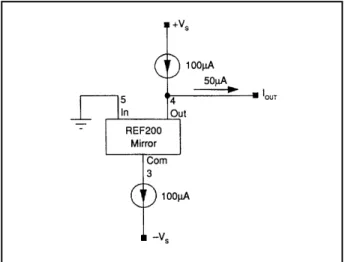
PIN STRAPPING REF200 FOR: 50µA CURRENT SINK
With a 100µA current source as a reference, it is simple to construct a current source of any value. The REF200 can be pin strapped for 50µA, 200µA, 300µA, or 400µA, in addi-tion to 100µA.
For a 50µA current sink, use the circuit shown in Figure 4. A 100µA current source is tied to the mirror common. Since a current mirror output must equal its input, 50µA flows in the input to ground, and the output is a 50µA current sink.
If compliance closer to the negative rail is needed for either the 50µA sink or source, use the circuit shown in Figure 6, or Figure 7. Here the mirror input is referenced to the negative rail with either a resistor and current source, or a resistor biased zener.
FIGURE 4. A 50µA Current Sink with compliance to ground can be made using one of the 100µA current sources and the mirror from the REF200.
FIGURE 6. Compliance of the 50µA Current Sink (Figure 5) can be extended to –VS+5V by referencing its bias point to the negative power supply rail using the other 100µA current and a resistor.
FIGURE 7. If you don’t have a current source to spare, the 50µA Current Sink with compliance to –VS+5V can be biased using a zener diode.
PIN STRAPPING REF200 FOR:
200µA FLOATING CURRENT SOURCE
A 200µA floating current source is formed by simply paral-leling the two current sources as shown in Figure 8. For compliance nearer to the negative rail, use the mirror as shown in Figure 9. The output of the mirror can swing about a volt closer to the negative rail than the current source alone.
PIN STRAPPING REF200 FOR: 50µA Current Source
For a 50µA current source, use the circuit shown in Figure 5. In this circuit a current sink subtracts 50µA from a second 100µA source leaving a 50µA source. Compliance is from below ground to within 2.5V of the positive rail.
FIGURE 5. A 50µA Current Source with compliance from ground to +VS –2.5V can be made using both 100µA current sources and the mirror from the REF200.
4 FIGURE 8. For a 200µA Floating Current Source simply
parallel the two 100µA current sources from the REF200.
FIGURE 10. The two 100µA Current Sources and Mirror in the REF200 can be connected to form a 300µA floating current source.
PIN STRAPPING REF200 FOR: 300µA Floating Current Source
A 300µA floating current source can be strapped together as shown in Figure 10. It is formed by paralleling a 200µA current source, made with one 100µA source and the mirror, with the other 100µA current source. The 200µA current source is made by connecting a 100µA current source to the mirror input so 100µA flows in the mirror output, and 200µA flows in the mirror common.
PIN STRAPPING REF200 FOR: 400µA Floating Current Source
A 400µA floating current source can be strapped together as shown in Figure 11. It is basically the same as the 200µA current source of Figure 10, except that 200µA is fed into the mirror input. This 200µA is summed with the 200µA that flows in the mirror output for a total of 400µA.
FIGURE 11. The two 100µA Current Sources and Mirror in the REF200 can be connected to form a 400µA floating current source.
FIGURE 9. You can mirror the 100µA or 200µA Current Sources from the REF200 for a 100µA or 200µA current sink with improved compli-ance.
RESISTOR PROGRAMMABLE CURRENT SOURCES AND SINKS
USING REF200 AND ONE EXTERNAL OP AMP: Current Source or Sink With Compliance to Power Supply Rail and Current Out >100µA
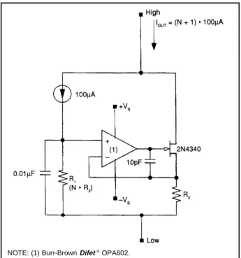
You can build a programmable current source of virtually any value using two resistors, an op amp, and a 100µA current source as a reference.
The current source shown in Figure 12 can be programmed to any value above the 100µA reference current. It has compliance all the way to the negative power supply rail. The 100µA reference forces a voltage of 100µA • R1 at the non-inverting input of the op amp. When using a Difet® op
amp as shown, input bias currents are negligible. The op amp forces the same voltage across R2. If R1 is N • R2, the output current is (N+1) • 100µA. So long as the op amps input common mode range and its output can swing to the negative rail within the voltage drop across R1, the current source can swing all the way to the negative rail. If the voltage drop across R1 is large enough, any op amp can
FIGURE 15. Current Sink.
Current Source or Sink With Any Current Out
For currents less than 100µA, use the circuits shown in Figures 14 and 15. They can be programmed for virtually any current (either above or below 100µA). In this case the 100µA current source forms a reference across R1 at the inverting input of the op amp. Since the reference is not connected to the output, its current does not add to the current output signal. So, if R1 is N • R2, then output current is N • 100µA. Because compliance of the 100µA current source is 2.5V, the current source, Figure 14, can only comply within 2.5V of the negative rail—even if the op amp can go further. Likewise the current sink, Figure 15, has a 2.5V compliance to the positive power supply rail. satisfy this requirement. Figure 13 shows the same circuit turned around to act as a current sink. It has compliance to the positive rail.
FIGURE 13. Current Sink. FIGURE 12. Current Source.
FIGURE 14. Current Source.
NOTE: (1) Burr-Brown® OPA602 or OPA128.
EXAMPLES
R1 R2 IOUT
100Ω 10MΩ 1nA ➜Use OPA128
10kΩ 1MΩ 1µA
10kΩ 1kΩ 1mA
NOTE: (1) Burr-Brown® OPA602.
FIGURES 14 and 15. If you don’t need compliance to the power supply rail, this circuit using a 100µA current source as a reference along with an external op amp and two programming resistors can pro-vide virtually any output current.
Current Sources and Sinks Using Voltage References
To make a current source with the best possible accuracy use a zener-based voltage reference. The REF200 uses a band-gap type reference to allow low voltage two-terminal opera-tion. Although this makes a more flexible general-purpose part with excellent performance, its ultimate temperature drift and stability cannot compare to the REF102 precision 10.0V buried zener voltage reference.
FIGURES 12 and 13. For a programmable current source with any output current greater than 100µA and compliance to +VS or – VS, use a 100µA current source as a reference along with an external op amp and two programming resistors.
6 FIGURE 15A. Current Source using Voltage Reference and Op Amp.
FIGURE 15B. Current Sink using Voltage Reference and Op Amp. Make a current source from a voltage reference using the circuit shown in Figure 15A. The voltage follower connected op amp forces the voltage reference ground connection to be equal to the load voltage. The reference output then forces an accurate 10.0V across R1 so that the current source output is 10V/R1.
Negative output compliance for the current source is limited by the op amp input common-mode range or output range (whichever is worse). When using the OPA111 on ±15V power supplies, the negative compliance is –10V. For com-pliance almost to the negative power supply rail, use a single-supply op amp such as the OPA1013.
Positive output compliance is limited by the voltage refer-ence minimum +VS requirement. When using the REF102 on
±15V power supplies, positive compliance is +3.5V. Make a current sink with a voltage reference using the circuit shown in Figure 15B. The op amp drives both the voltage reference ground connection and the current scal-ing register, R1, so that the voltage reference output is equal to the load voltage. This forces –10.0V across R1 so that the current sink output is –10V/R1. The R2, C1 network pro-vides local feedback around the op amp to assure loop stability. It also provides noise filtering. With the values shown, the reference noise is filtered by a single pole with f–3dB = 1/(2 •π• R2• C1).
Negative output compliance for the current sink is limited by the op amp and further reduced by the 10V drop across R1. When using the OPA111 on ±15V power supplies, negative compliance is only guaranteed to ground. When using the single-supply OPA1013 op amp, negative compliance is approximately –5V.
Positive compliance is limited by the REF102, but is im-proved by the 10V across R1. For a REF102 operating on
±15V power supplies, the positive compliance is +10V (limited by the op amp common mode input range). Keep in mind that the ultimate accuracy of a voltage refer-ence based current source depends on the absolute accuracy of the current-scaling registor. The absolute TCR and stabil-ity of the resistor directly affect the current source tempera-ture drift and accuracy. This is in contrast to circuits using current source references, as shown in Figures 12 to 15, where accuracy depends only on the ratio accuracy of the resistors. It is much easier to get good resistor ratio accuracy than to get good absolute accuracy especially when using resistor networks.
Although these current sources made with voltage references do not have the compliance range of the previous circuits, they may be the best choice where the utmost in accuracy is required.
Floating Current Source With Current Out > 100µA
If a completely floating programable current source is needed, use the circuit shown in Figure 16. It is basically the same as the current source shown in Figure 12 except that R2 is driven by a MOSFET. Since no current flows in the gate of the MOSFET or the inputs of the op amp, all current that enters the resistors (and no more) leaves. Therefore the current source is completely floating.
The power supplies of the op amp in this circuit, as in the other circuits, must be connected to ±VS. Also, the input and output common mode limitations of the op amp must be observed.
FIGURE 16. Use a 100µA Current Source as a reference, an external op amp, two programming resistors, and a series pass element for a programmable floating curent source.
NOTE: (1) Burr-Brown Difet® OPA602.
Notice that since a current source is used as a reference, the circuit can also be used as a precision current mirror. Unlike mirrors which use matched transistors, this mirror remains highly accurate no matter what the mirror ratio.
The pass element can bipolar, JFET, MOSFET, or a combi-nation. The examples recommend MOSFETS because their low gate current minimizes output error. Also, MOSFETs with very high current ratings are available, and require no additional drivers.
In many cases bipolar devices are adequate and may be preferred due to their low cost and availability. With a bipolar device, the base current will add error to the output signal as discussed in the cascoding section. Using a darling-ton-connected bipolar device feeds the error current back into the signal path and reduces the error by the forward current gain (beta) of the input transistor.
In some high temperature applications, darlington-connected bipolar transistors may have lower error than FETs. As a rule of thumb, the gate current of a FET or MOSFET doubles for every 8°C increase in temperature, whereas the beta of a bipolar device increases approximately 0.5%/°C. Therefore, when operating at 125°C, the gate current of a FET will be about 6000 times higher than at 25°C, while the base current of the bipolar will be 1.5 times lower. When selecting the op amp for this application, pay particu-lar attention to input bias current, input common mode range, and output range.
The bias current of the op amp adds to the input current, and subtracts from the output current. For a 1:1 mirror applica-tion, the error is only the mismatch of bias currents or IOS of the amplifier. For other ratios, assume that the error is equal to the full amplifier bias current. For most applications, the error will be negligible if a low bias current Difet®amplifier
such as the Burr-Brown OPA602 is used. Its IB is 1pA max. Be sure to observe the input common mode range limit of the op amp. For example, when using the OPA602 in a current sink application, the voltage between the op amp negative supply and its input must be at least 4V. In a split power supply application, R1 and R2 can be connected to ground, and the op amp negative supply can be connected to –5V or –15V and there is no problem. In a single supply application, or when R1, R2, and the op amp’s –VS are all connected to the negative power supply, a drop of at least 4V must be maintained across R1.
Using a single supply op amp allows the input common mode range to go to 0V. Especially in single supply current mirror applications, it is often desirable for the input and output to go to zero. The OPA1013 has an input common-mode range which extends to its negative power supply, and its output will swing within a few mV of the negative supply. Although the OPA1013 has bipolar inputs, its bias current is low enough for most applications.
Components R3, R4, and C1 form a compensation network to assure amplifier stability when driving the highly capacitive inputs of some MOSFETs. In many applications they can be omitted.
Current Sources and Sinks and Current Mirrors Using an Amplifier and a Series Pass Element
In some applications it may be desirable to make a current source or sink using a series pass element in addition to an op amp. This approach provides the benefits of cascoding and also allows arbitrarily high current outputs.
The circuit used is the same as for the programmable floating current source shown inFigure 16.The difference is that the op amp power supply connection and reference input are both returned to a fixed potential. The result is either a current source or sink, but not a floating current source. The advantage is that the output can be any value, either more than, less than, or equal to the input reference. Also, a voltage source or even a variable voltage input can be used as a reference. The examples shown in Figures 17 through 20 show 100µA current sources used as references.
8 FIGURE 17. Programmable Current Sink using series pass device.
FIGURE 18. Sinking Current Mirror using series pass device.
NOTE: Can be connected to –VS with 4V min across R1.
FIGURE 19. Programmable Current Source using series pass device.
N channel enhancement MOSFET Supertex, Siliconix, Motorola, etc. or
2 x 2N2222
N channel enhancement MOSFET Supertex, Siliconix, Motorola, etc.
or 2 x 2N2222
Supertex, Siliconix, Motorola, etc. P channel enhancement MOSFET or
2 x 2N3906
NOTE: Can be connected to +VS with 2V min across R1.
NOTE: The LF155 input common-mode range typically includes +VS,
but this is not a guaranteed specification.
quiescent current flowing from its negative supply pin sums into the current flowing into R2. The op amp outputs drive
the additional current needed through R2 so the voltage drop across it matches the voltage drop across R1. If R1 is N • R2, the output current is (N+1) • 100µA. With the values shown, the output current is 25mA.
The op amp outputs are connected to R2 through 100Ω resistors. The current delivered by A1 produces an approxi-mate 0.5V voltage drop across R3. The other three op amps are connected as voltage followers so that the same voltage is dropped across the other three 100Ω resistors. The output current from each op amp is therefore equal and the load is shared equally. This technique allows any number of 10mA output op amps to be paralleled for high output current.
CASCODING CURRENT SOURCES FOR IMPROVED OUTPUT IMPEDANCE, HIGH FREQUENCY PERFORMANCE, AND HIGH VOLTAGE COMPLIANCE Cascoding With FETs
The output impedance and high frequency performance of any current source can be improved by cascoding. Starting with a precision current source like the REF200 or any of the variations previously discussed, it is relatively easy to build a current source to satisfy just about any need.
Cascoding can also be used to increase high voltage compli-ance. High voltage compliance of a cascoded current source is limited solely by the voltage rating of the cascoding device. High voltage compliance of hundreds or even thou-sands of volts is possible.
Cascoding is the buffering of the current source from the load by a series pass device as shown in Figure 22. Here an N channel JFET cascodes the current source from the output. The gate of the JFET is tied to ground, its source to the current source, and its drain to the load. Variations in the load voltage are taken up by the drain of the JFET while the source voltage remains relatively constant. In this way, the voltage drop across the current source remains constant regardless of voltage changes across the load. With no changes in the voltage across the current source, and with no current lost through the JFET drain approaches infinity. AC performance of the cascoded current sink approaches that of the JFET.
Floating Current Source With Current Out >100µA and No Separate Power Supply
If a programmable current source is needed, and no separate power supply is available, consider the floating current source shown in Figure 21. Here the op amp power supplies are connected to the current source input terminals. The op amp quiescent current is part of the output current.
FIGURE 20. Sourcing Current Mirror using series pass device.
Supertex, Siliconix, Motorola, etc. P channel enhancement MOSFET or
2 x 2N3906
There are two special requirements. First, a single supply op amp must be used (an op amp with an input common mode range that includes the negative supply rail). Also the output current must be greater than the op amp quiescent current. The circuit is basically the same as Figure 12. The 100µA current flowing through R1 produces a floating voltage reference at the non-inverting input of A1. The op amp FIGURE 21. 25mA Floating Current Source using a quad single-supply op amp needs no external power supply.
10 Since the gate of the JFET is tied to ground, the output compliance is limited to near ground. If greater compliance is required for the current sink, the gate of the JFET can be referenced a few volts above the negative rail as shown in Figures 23 and 24. In Figure 23 the gate reference is derived from a resistor biased from the second current source. If a current source is not available, use a resistor biased zener as shown in Figure 24.
FIGURE 24. Cascoded Current Sink with compliance to – VS+5V (using zener diode for bias).
FIGURE 23. Cascoded Current Sink with compliance to – VS+5V (using zener diode for bias).
To implement current sources, turn the circuits around and use P channel JFETs as shown in Figures 25 through 27.
FIGURE 26. Cascoded Current Source with compliance to – VS+5V (using current source and resistor for bias).
FIGURE 27. Cascoded Current Source with compliance to – VS+5V (using zener diode for bias).
In most applications, JFETs make the best cascoding devices, but bipolar transistors and MOSFETs can also be used. MOSFETs can provide equivalent AC and DC performance to JFETs. Bipolar devices may offer better high frequency performance, but have a limited DC output impedance. The output impedance of a bipolar cascoded current source is limited by changes in base current with changes in collector voltage. The maximum output impedance of a bipolar cas-coded current source is b • RO, where b is the current gain of the bipolar device, and RO is its output impedance
FIGURE 25. Cascoded Current Source with compliance to ground.
FIGURE 22. Cascoded Current Sink with compliance to ground.
200µA Floating Cascoded Current Source Using REF200
Floating cascoded current sources with typical output im-pedances exceeding 10GΩ can be easily implemented. Us-ing the REF200 and a few external devices, sources of 200µA, 300µA, and 400µA can be strapped together. The 200µA floating cascoded current source is shown in
Figure 28. It is made using a cascoded current source and a cascoded current sink each biasing the other. Low voltage compliance is limited to about 8V by the sum of the gate reference voltages. High voltage compliance is limited by the lower voltage rated FET.
Regulation (15V–30V) = 0.00005%/V (10GΩ)
FIGURE 28. Cascoded 200µA Floating Current Source.
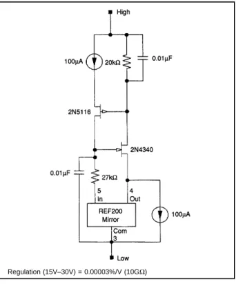
300µA Floating Cascoded Current Source Using REF200
The 300µA floating current source is shown in Figure 29. It is similar to the 200µA current source shown in Figure 28, except the current source in the cascoded sink section is derived from the mirror. The gate reference for the sink cascode is derived from the series combination of the mirror input and a 27kΩ resistor. The extra 100µA is obtained by summing the other 100µA current source into the sink cascode device. Compliance limits are the same as for the 200µA cascoded source.
400µA Floating Cascoded Current Source Using REF200
The 400µA floating cascoded current source is shown in Figure 30. It is the similar to the 300µA cascoded current source, except that the mirror is driven by a cascoded 200µA current source derived by the parallel combination of the two current sources in the REF200. The low voltage compli-ance of this circuit is about 1V better than the previous two circuits because the mirror compliance is about 1V better. High voltage compliance is still limited only by the break-down of the lower rated FET.
Regulation (15V–30V) = 0.00003%/V (10GΩ)
FIGURE 29. Cascoded 300µA Floating Current Source.
Regulation (15V–30V) = 0.00025%/V (10GΩ)
FIGURE 30. Cascoded 400µA Floating Current Source.
NOISE REDUCTION OF CURRENT SOURCES
In many modern systems, noise is the ultimate limit to accuracy. And in some systems, performance can be im-proved with a lower noise current source. Current source noise can be reduced by filtering, using the same basic principals used for noise reduction of voltage references. Reducing the noise bandwidth by filtering can reduce the total noise by the square root of the bandwidth reduction.
12 The value of the resistor used in the noise reduction circuit determines its ultimate performance. Although the noise of the resistor increases with the square root of its value, its noise degenerating effect reduces noise linearly. Therefore, the noise is reduced by the square root of the resistor increase. The practical limit for the noise reduction is the voltage drop which can be placed across the resistor. Mathematically, current noise due to the resistor is the resistor thermal noise divided by the resistor value.
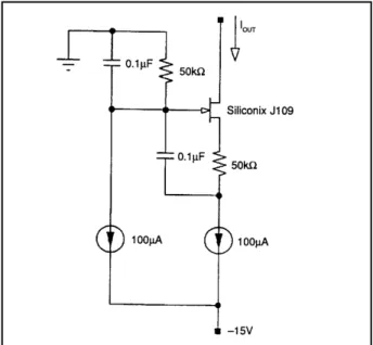
With a 50kΩ resistor, the minimum theoretical noise is .6pA/√Hz, with 10kΩ, it is 1.3pA/√Hz. Noise measurements of the circuit using both 10kΩ and 50kΩ resistors and the Siliconix J109 FET agree with these theoretical numbers within 20%.
The noise reduction circuit in Figure 31 has a low voltage compliance limit near ground. For compliance below ground, use the circuit shown in Figure 32.
One current source noise reduction circuit is shown in Figure 31. It is basically a FET cascode circuit with the addition of an RC noise filtering circuit. The FET, as biased by the 100µA current source, forces an accurate DC voltage across the circuit.
Without the capacitor, noise from the current source would feed directly through to the output. The capacitor filters the noise at a –3dB frequency of 1/(2 • π • R• C), or about 30Hz in this example. Filtering below this frequency will not reduce noise further, since the 30Hz pole is already below the 1/f corner of the current source, and noise can not be reduced by filtering in the 1/f region. Also, the noise of the FET and resistor are not filtered. Still, using this circuit, the noise is reduced from the typical 20pA/√Hz to less than 1pA/√Hz.
FIGURE 32. Current Noise Filtering Circuit with compli-ance below ground.
In addition to noise reduction, these circuits have the other advantages of a FET cascoded current sink; output imped-ance in the GΩ region, improved AC performance, and high voltage compliance limited only by the FET.
APPLICATIONS OF FIXED
CURRENT SOURCES
VOLTAGE REFERENCES USING CURRENT SOURCES
Many design problems can be easily solved with inexpen-sive, easy-to-use current sources like the REF200. Although applications are endless, the collection of circuits that fol-lows is intended to stimulate your thinking in several broad categories: fixed voltage references, floating voltage refer-ences, current excitation, fixed current referrefer-ences, steered current references, and biasing.
Current sources are a versatile means of forming voltage references. Why not just use a voltage reference? With a current source, a single resistor provides a programmable voltage source of any value. Low voltage references are often needed, and with this approach, it’s as easy to get a 1mV reference as it is to get a 10V reference. Also, the voltage can be referenced anywhere—to the positive rail, the negative rail, or floating anywhere in between.
When impedances driven by the voltage reference are high, the voltage output from the resistor derived voltage refer-ence can be used directly. The 100µV reference shown in Figure 33 can be used directly in voltage-to-frequency converter (VFC) auto-zero applications where an off-zero reference is needed (since zero frequency would take forever to measure, off-zero techniques are often used for calibrat-ing VFCs). Where a lower output impedance is needed, a simple buffer can be added as shown in Figure 34. IR NOISE= 1.3 • 10 –10
(
)
R R = 1.3 • 10 –10(
)
/ RFIGURE 31. Current noise from a current source can be filtered using this circuit.
FIGURE 33. 100µV Reference for VFC off-zeroing.
FIGURE 34. Buffered Voltage Reference.
For a floating voltage reference, simply drive the reference low side (grounded side of the voltage-setting resistor) as shown in Figure 34A. Notice that in addition to the swing limitations imposed by the op amp input common-mode range and output range, the reference high side swing is limited to 2.5V from the positive rail by the REF200's minimum compliance voltage. The low side swing is limited only by the op amp. If the reference voltage is more than about 3V this limitation can be eliminated by adding gain as shown in Figure 34B. In this example, the 1V across the reference setting-registor is amplified to 5V at the output. Since there is always 4V between the output and the op amp inputs, the high-side swing is not limited by the current source compliance or the op amp input common mode range. It is limited only by the op amp out put swing capability.
Where the voltage reference is lower than about 3V, the high side compliance will still be limited by the current source compliance. In these situations, consider the circuit shown in Figure 34C. In this case, the op amp noninverting input is driven while the current source connects to the other op amp input and a voltage setting resistor with its other terminal
connected to the output. High-side compliance is limited only by the op amp. Another advantage of this circuit is its high input inpedance. The disavantage is limited low side compliance. Current source compliance limits swing to the negative rail to 2.5V — regardless of the op amp input common mode range.
FIGURE 34A. Floating Voltage Reference.
FIGURE 34B. Floating Voltage Reference with high-side compliance limited only by op amp output swing capability.
FIGURE 34C. Floating Low Voltage Reference with high impedance input drive and high-side output compliance limited only by op amp output swing capability.
14
FIGURE 35. Op Amp Offset Adjustment Circuit uses the two 100µA current sources from a REF200 to provide accurate ±5mV references.
FIGURE 36. Op amp offset adjustment circuit using Bourns Trimpot®.
OP AMP OFFSET
ADJUSTMENT USING 5mV REFERENCE
Op amp offset adjustment circuits are another application for millivolt level references. Many op amps, especially duals and quads, have no built-in provision for offset adjustment. Even when offset adjustment pins are provided, using them can degrade offset voltage drift and stability (e.g. the drift of a typical bipolar input op amp is increased 3µV/°C for each millivolt of offset adjustment). External offset adjustment circuits are commonly used to solve these problems. Conventional external offset adjustment circuits can add problems of their own. Many of these circuits use the op amp power supplies as references. Power supply variation feeds directly into the op amp input. This error appears as poor power supply rejection. Likewise, noise from the power supplies appears as op amp input referred noise.
The circuits shown in Figures 35 and 36 solve these prob-lems. REF200 current sources provide regulated ±5mV references for stable offset adjustment. This approach pro-vides a truly precision offset adjustment free from problems associated with power supply variations, noise, and drift. The circuit shown in Figure 35 uses a pair of 51Ω resistors connected to ground to establish the ±5mV reference. A pot connected across this reference allows a ±5mV offset adjust-ment range. Additional pots can be connected, but be sure to maintain a parallel resistance >50Ω to get >±5mV range. The second circuit, Figure 36, uses a special potentiometer manufactured by Bourns. It is especially designed for op amp offset adjustment. It has a tap at the center of the element which can be connected to ground. Using this connection eliminates the 51Ω resistors needed in the first circuit.
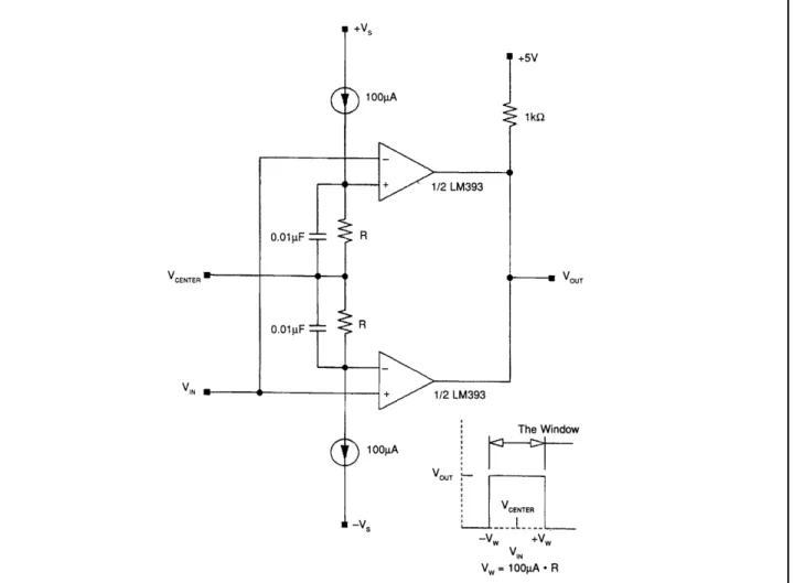
WINDOW COMPARATOR USING FLOATING VOLTAGE REFERENCE
The window comparator circuit, Figure 37, is an example of a floating reference application. Here, a pair of current sources is used to provide a floating bipolar window voltage driven by the VCENTER input. VO is low when VI is either above VCENTER + 100µA • R, or below VCENTER – 100µA • R. Otherwise, VO is high. By using different values for the programming resistors, the threshold can be set asymmetri-cally around VCENTER if desired.
RTD EXCITATION USING CURRENT REFERENCE
Current sources are often used for excitation of resistor type sensors such as RTDs. If the RTD is located remotely, as it often is, voltage drops in the interconnecting wire can cause
excessive errors. The usual solution to this problem is to use four wire Kelvin connections. Two wires are used to carry the current excitation signal to the RTD. The other two wires sense the voltage across the RTD. With no current flowing in the sense connection, there is no error due to wire resistance.
One problem is that the additional wiring can be very expensive. The three wire circuit shown in Figure 38 saves one wire. 200µA is used for excitation of a 1kΩ RTD, and a matching current from the current mirror is forced in the ground connection. The voltage drops through the two wires cancel thereby eliminating error.
Notice also, that one common wire (shown as a shield) can serve multiple sensors. Each additional RTD only needs one additional pair of wires.
16
FIGURE 38. RTD excitation with three-wire lead resistance compensation.
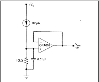
FIGURE 39. Precision positive dead-band circuit.
DEAD BAND CIRCUITS
USING CURRENT REFERENCE
Servo control systems frequently use dead-band and limiting circuits. The precision dead-band circuit shown in Figures 39 and 40 demonstrates the use of a current source as a fixed reference. To understand how it works, notice that, without the current reference, the circuit is an inverting half wave rectifier. Positive inputs drive the op amp output negative and feedback is through forward biased D1. No current flows through reverse biased D2, and the output is held at virtual ground by R2.
Negative inputs forward bias D2 and drive the output posi-tive. Feedback to the output through R2 eliminates error due to the diode drop, and the circuit functions as a precision
unity gain inverter (VO = –VI). (Adding the current reference pre-biases to the input so that the output remains at virtual ground until the input current through R1 exceeds 100µA.) The output is zero (dead) until VI < ±100µA • R1. An alternate approach would be to pre-bias the input through a precision resistor connected to a voltage reference, but that would add noise gain increasing offset, drift, and noise at the output.
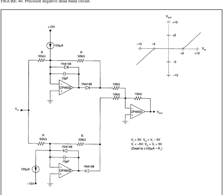
For a negative dead-band use the circuit shown in Figure 40. It’s the same circuit with the diodes reversed.
For a double dead-band, use the circuit shown in Figure 41. It uses both the positive and negative dead-band circuits summed together by a third amplifier.
FIGURE 41. Precision double dead-band circuit. FIGURE 40. Precision negative dead-band circuit.
18
BIDIRECTIONAL CURRENT SOURCES
One of the advantages in working with currents is that they can be steered by diodes or switches without error. As long as no current is lost through leakage, voltage drops in series with current signals do not diminish their accuracy. The bidirectional current source shown in Figure 42 is a versatile circuit building block and an excellent example of diode steering. This two-terminal element is basically a full-wave bridge rectifier circuit with a current source connected between its DC terminals. A positive signal on the left terminal with respect to the right reverse biases D3 and D4 and accurately steers current through D1 and D2. A negative signal reverses the situation and accurately steers the same current in the opposite direction.
For one diode drop better compliance, use the bidirectional current source shown in Figure 43. The disadvantages of this circuit are that two current sources are required, and the inherent current matching of the previous circuit is lost.
FIGURE 42. Bidirectional current source.
FIGURE 43. Bidirectional current source with improved compliance.
When R1 is added, the circuit still functions as a follower for small signals where the current through R1 is less than 100µA. When the current reaches 100µA, the current source becomes active and limits the output voltage. With the bidirectional current source, the circuit limits symmetrically in both directions.
LIMITING CIRCUITS USING
BIDIRECTIONAL CURRENT SOURCES
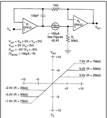
The precision double limiting circuit shown in Figure 44 puts the bidirectional current source to work. To understand how this circuit works, notice that without R1, it functions as a precision unity-gain amplifier. The input signal is con-nected to the non-inverting terminal of A1. Feedback to the inverting terminal is through the bidirectional current source, voltage-follower connected A2, and the 1kΩ resistor. When less than 100µA is demanded from the current source, it saturates and the total voltage drop across the bidirectional current source is less than about 2V plus two diode drops. Since no current flows in the 1kΩ resistor, the circuit output voltage must equal the input voltage and errors due to A2 and the drop across the current source are eliminated. The 1k-100pF network provides compensation for the extra phase shift in the feedback loop.
FIGURE 44. Precision double limiting circuit.
If a limit in just one direction is required, replace the bidirectional current source with a current source and single diode as shown in Figure 45. For limiting in the opposite direction, reverse the polarity of the current source and diode.
PRECISION TRIANGLE WAVEFORM GENERATOR USING BIDIRECTIONAL CURRENT SOURCES
The precision triangle waveform generator shown in Figure 46 makes use of two bidirectional current sources. One steers a precision current signal into the integrating capacitor connected to the inverting input of the op amp. The other steers a precision current into the 10kΩ resistor connected to the positive op amp terminal to provide ±1V hysteresis. The result is a relaxation oscillator with precision triangle and square wave outputs of ±1V.
DUTY CYCLE MODULATOR USING BIDIRECTIONAL CURRENT SOURCES
The precision duty cycle modulator shown in Figure 47 is a variation of the triangle generator. Here the integrating capacitor is replaced by a true integrator formed by A1 and C. This allows the summation of a ground referenced signal through the 100kΩ input resistor. With no input signal, the output is a square wave with 50% duty cycle. Input signals sum into the integrator through the 100kΩ resistor. The integrator then slews faster in one direction, and slower in the other. The result is a linear duty cycle modulation of the output signal. The modulator is said to be duty cycle rather than pulse width because the output frequency varies some-what with input signal. For a constant frequency duty cycle modulator add a resistor in series with the inverting input of A2 and drive that input with a resistor coupled clock signal.
FIGURE 46. Precision triangle waveform generator.
20
ment is critical. While single supply op amps have been available for many years, single supply IAs have not. What’s more, single supply IAs can not be made by simply using single supply op amps in the traditional manner. In a con-ventional IA topology the outputs as well as the inputs would need to swing to the negative rail. Although some op amps come close, no amplifier output can swing all the way to its power supply rail, especially when driving a load. The single supply IA circuit shown in Figure 49 solves this problem by simply level shifting the input signal up by a Vbe with a matched pair of matched PNP input transistors. The transistors are biased as emitter followers by the 100µA current sources in a REF200. The ensuing circuit is a traditional three op amp IA. OPA1013s are used for input amplifiers because they are designed for single supply op-eration and their output can also swing near the negative rail. The Burr-Brown INA105 is used as a difference amplifier. All critical resistor matching is taken care of by the INA105. The common mode range of the single supply IA typically extends to 0.5V below the negative rail with a typical CMR better than 86dB.
VOLTAGE CONTROLLED
CURRENT SOURCE USING INA105
The modified Howland current pump (Figures 50-52)is an extremely versatile voltage controlled current source. Since it has differential inputs, you can ground one input and drive the other to get either an inverting or noninverting transfer function. If you drive both inputs, the output current will be proportional to the voltage difference between the inputs. What’s more, unlike current sources made with a series pass element, which can either sink or source current, this current source has a bipolar output. It can both sink and source current.
Notice that the duty-cycle modulator has a true integrating input. This is in contrast to conventional modulators which simply use a comparator connected between the input signal and a precision triangle wave. With the conventional ap-proach, at crossing, input noise feeds through at the com-parator bandwidth resulting in jitter. Not only does the integrating input filter out input noise, it can be synchro-nized to input noise (such as 60Hz), completely notching out its effect. If integration takes place over one or more com-plete cycles of the noise signal, the undulations of the noise signal are exactly averaged out.
SLEW RATE LIMITER
In some applications, especially when driving inductors, it is necessary to limit the signal slew rate. The rate limiting circuit shown in Figure 48 uses a diode bridge for current steering in a different way. Here two current sources are connected, one to the positive terminal and one to the negative terminal, of the bridge. Without the capacitor, the circuit would act as a unity gain inverting amplifier. Feed-back through the 10kΩ– 10kΩ resistor network drives the left side of the bridge. The right side of the bridge follows, driving the op amp inverting input. Voltage offset due to diode mismatch can be mitigated by using a monolithic bridge such as the one specified. When the integrator capaci-tor is added, charging and discharging current must flow to maintain the virtual ground. But when that current exceeds 100µA, the bridge reverse biases limiting the output slew rate to 100µA/°C regardless of input signal rate.
SINGLE SUPPLY INSTRUMENTATION AMPLIFIER
Single power supply systems are common and the need for instrumentation amplifiers (IAs) to operate in this
Use of this circuit was limited in the past due to the critical resistor matching and resistor TCR tracking requirements. By using the INA105 difference amplifier, the circuit can be easily implemented with the addition of two 1% resistors. Matching of the external resistors is important, but since they add to the internal 25kΩ resistors, the matching require-ment is divided down by the ratio of resistance.
Output impedance of the current source is proportional to the common mode rejection (CMR) of the difference fier. Mismatch of feedback resistors in the difference
ampli-fier caused by the external resistors will degrade CMR and lower the current source output impedance. Resistor match of 0.002% is required for 100dB CMR in a unity gain difference amplifier. Depending on the value of the external resistor and output impedance requirement, it may be neces-sary to trim the external resistor.
When the value of the external resister becomes large consider the alternate circuit shown in Figure. 51.
FIGURE 51. Voltage-controlled current source with differ-ential inputs and bipolar output and circuit to eliminate feedback resistor error.
FIGURE 49. Single-supply instrumentation amplifier.
FIGURE 50. Voltage-controlled current source with differ-ential inputs and bipolar output.
22 You need an extra amplifier to drive the feedback resistor in the difference amplifier, but only one external resistor is required, and no matching or trimming is needed.
In any case the output impedance of the current source can be approximated by the following relationship:
ZO = RX • 10 [CMRR/20]
Where:
ZO = equivalent output impedance of current source [Ω] CMRR = difference amp common mode rejection ratio [dB]
(for Figure 50)
RX = parallel combination of external resistor and 25kΩ R • 25kΩ
RX = ———————— R + 25kΩ (for Figure 51)
RX = external resistor [Ω]
The INA105 can source 20mA and sink 5mA. If higher output current is required, add a current buffer as shown in Figure 52. The OPA633 shown allows output currents up to
±100mA. Since the buffer is within the feedback loop, its DC errors have no effect on the accuracy of the current source. When using other buffers make sure that their bandwidth is large enough not to degrade circuit stability. If you want voltage gain in the voltage to current converter, use the INA106 for a gain-of-ten difference amplifier. Don’t forget that source impedance adds directly to the input resistors of the difference amplifier which can degrade its performance. A source impedance mismatch of 5Ω will degrade the CMRR of the INA105 to 80dB. If you are driving the circuit from an amplifier or other low impedance source, this should not be a problem. If you have higher source impedances, buffer the driven input(s) of the differ-ence amplifier, or use an instrumentation amplifier such as the INA110 instead of a difference amplifier.
VOLTAGE CONTROLLED CURRENT SOURCE WITH INSTRUMENTATION AMPLIFIER INPUT —THE XTR101
The XTR101 is a floating current source designed for two wire 4-20mA current loop applications. It is a voltage controlled current source with a precision instrumentation amplifier input. It also contains two matched 1mA current sources which makes it suited for remote signal conditioning of a variety of transducers such as thermocouples, RTDs thermistors, and strain gauge bridges.
Figure 53 shows the XTR101 connected as a temperature controlled current source. The temperature sensing element is a thermocouple, and cold junction compensation is pro-vided by the diode.
The product data sheet for the XTR101, (PDS-627) gives operating details for the device and shows several other applications.
SINGLE SUPPLY VOLTAGE
CONTROLLED CURRENT SOURCE—THE XTR110
The XTR110 is a precision single supply voltage to current converter. Although it is designed specifically for three wire 4-20mA current transmission it can also be used in more general voltage to current source applications. As shown in Figure 54, it contains: a precision 10.0V reference and input resistor network for span offsetting (0V In = 4mA Out), a voltage to current converter for converting a ground refer-enced input signal to an output current sink, and a current mirror for turning the output of the current sink into a current source.
The current mirror has a gain ratio of 10:1 and uses an external pass transistor to minimize internal thermal feed-back and improve accuracy. Since the mirror transistor is external, an external mirror ratio setting resistor can be added for an arbitrarily high output current.
Both the voltage to current converter, and the current mirror use single supply op amps so that the input and output signals can go to zero. In the case of the mirror op amp, the common mode range goes to the positive power supply rail rather than common.
The following table shows a range of input-output spans that is available simply by pin strapping the XTR110.
Input Output
Range Range Pin Pin Pin Pin Pin
(V) (mA) 3 4 5 9 10
0-10 0-20 Com Input Com Com Com
2-10 4-20 Com Input Com Com Com
0-10 4-20 +10 Input Com Com Open
0-10 5-25 +10 Input Com Com Com
0-5 0-20 Com Com Input Com Com
1-5 4-20 Com Com Input Com Com
0-5 4-20 +10 Com Input Com Open
0-5 5-25 +10 Com Input Com Com
For more details and applications, request product data sheet PDS-555.
FIGURE 52. Voltage-controlled current source with differ-ential inputs and current boosted bipolar out-put.
FIGURE 53. Temperature-controlled current source using XTR101.
24
Matching resistor, RM, preserves the resistance match of the INA105 and maintains its high common-mode rejection (CMR). Because 100Ω is small compared to the 25kΩ difference resistors, a 1% tolerance is sufficient to maintain 86dB CMR.
The INA105 references the output signal to ground with a gain of one. For a 0-10mA input the output is 0 to –1V (a transfer function of –100V/A). If a positive transfer function is desired, interchange the input pins of the difference amplifier. To reference current signals to the positive rail, simply connect the sense resistor and the other difference amplifier input to that point.
The 25kΩ input impedance of the difference amplifier causes a slight error by shunting a portion of the input current signal. In the noninverting configuration, the match-ing resistor lowers the difference amplifier gain, but since the shunting input impedance of the noninverting input is 50kΩ, for a unity gain difference amp, the error turns out to be the same. For a 100Ω sense resistor, the error is a approximately 0.4%. For better accuracy, select a slightly higher value sense resistor to compensate for the error according to the following equation.
25k • X RS = RM = ———————
25k – X Where:
X = desired transfer function [V/A] For example:
For 1V/10mA (100V/A) from Figure 55: RS = RM = 100.4Ω
POWER AMP LOAD CURRENT
MONITORING USING THE INA105 OR THE INA117
The INA117 is a difference amplifier similar to the INA105 except that it has a 20/1 input divider allowing a ±200V common mode input range. It also has an internal gain of 20 providing an overall gain of one. The penalty is that ampli-fier DC errors, and resistor and ampliampli-fier noise are amplified by 20. Still for 200V applications that do not require gal-vanic isolation its has better performance than isolation amplifiers, and it does not require an isolated power supply. Figure 56 shows a circuit for measuring load current in a bridge amplifier application using the INA117. At low frequencies, a sense resistor could be inserted in series with the load, and an instrumentation amplifier used to directly monitor the load current. However, under high frequency or transient conditions, CMR errors would limit accuracy. This approach eliminates these problems by gleaning the load current from measurements of amplifier supply current. The power supply current of one of the bridge op amps is measured using INA117s and 0.2Ω sense resistors con-nected to the power supplies. Because the 0.2Ω sense resis-tor adds negligible resistance error to the 380kΩ input resistors of the INA117s, no matching resistors are required.
CURRENT RECEIVER WITH COMPLIANCE TO BOTH POWER SUPPLY RAILS USING THE INA105
Measuring current signals can be as simple as feeding the current into a precision resistor (V = I • R). If needed, the voltage developed across the resistor can be buffered or amplified with an operational amplifier.
If common-mode signals are present on the current return end of the sense resistor, an instrumentation amplifier (IA) can be used to reject the common mode signal and reference the output signal to ground. However, a limitation of con-ventional IAs is that their common mode input range is limited to less than 10V.
When you need to reference the current return of the sense resistor to a higher common mode voltage, consider one of the following difference amplifiers.
Input Common Other
Model Mode Range Features
(1)
INA105 ± 20V
INA117 ±200V
RCV420 ± 40V (2)
Figure 55 shows a current receiver using the INA105. The input current signal is sensed across 100Ω resistor, RS, connected to the negative power supply rail. Connecting the sense resistor to a power supply rail instead of ground maximizes the voltage drop available across the current transmitter.
Voltage divider action of the feedback resistors within the INA105 divide the common-mode input by two. Therefore, common mode input signals of up to ±20V are attenuated to an acceptable level of no more than ±10V at the op amp inputs.
NOTES: (1) Common-mode input range specified for operation on standard
±15V power supplies. (2) Also contains a precision reference and offsetting circuitry to get 0-5V outputs with 4-20mA inputs.
FIGURE 55. Current-to-voltage converter referenced to the negative power supply rail.
FIGURE 56. Bridge amplifier load current monitor using the INA117. To understand how the circuit works, notice that since no
current flows into the inputs of A1: ILOAD = I1 – I2 If R1 = R2 = R Then e1 = I1 • R, e2 = –I2 • R, and e1 + e2 = ILOAD • R
The INA105 is connected as a noninverting summing ampli-fier with a gain of 5 (the accurate matching of the two 25kΩ input resistors makes a very accurate summing amplifier). Then
eO = 5(e1 + e2) = 5(ILOAD • R), since
R = 0.2Ω, eO = ILOAD [1V/A]
4 to 20mA CURRENT LOOP RECEIVER WITH 0 to 5V OUTPUT USES THE RCV420
The RCV420 is a current-to-voltage converter designed specifically for conversion of 4-20mA input currents into 0-5V outputs. A pair of precision 75Ω sense resistors are provided internally allowing both inverting and noninverting transfer functions. Input common mode signals up to ±40V can be accommodated due to the internal 4/1 input attenua-tor. Also, the precision 10.0V reference used for span offseting is available to the user.
Figure 57 shows a typical application. For more details and applications, request product data sheet PDS-837.
VIRTUAL GROUND
CURRENT-TO-VOLTAGE CONVERTER
When current-to-voltage conversion with no voltage burden is needed, used the transimpedance amplifier Figures 58— 61. In this circuit, an op amp drives the current input node to virtual ground by forcing a current equal to IIN through the feedback resistor, RFB. Notice that the transfer function is inverted:
26
FIGURE 58. Virtual ground current-to-voltage converter. FIGURE 59. Virtual ground current-to-voltage converter redrawn to Illustrate phase delay due to input capacitance and feedback resistor.
FIGURE 57. 4-20mA current loop receiver using the RCV420.
NOTE: (1) May Connect to Gnd or up to ±40V.
The feedback capacitor, CFB, may be needed for circuit stability. To see why, consider the redrawn circuit, Figure 59. CIN represents the input capacitance of the circuit and includes input source capacitance, and op amp input capaci-tance. Notice that RFB and CIN form a single pole filter in the feedback path to the op amp input. Phase delay through this circuit subtracts from the op amp phase margin which may result in instability, especially with the large values of RFB often used in these circuits. If CFB≥ CIN, the phase delay will be less than 20° assuring stability with most unity-gain-stable amplifiers.
PHOTODIODE AMPLIFIER USING VIRTUAL GROUND I/V CONVERTER
The photodiode amplifier shown inFigure 60 is a common application of the transimpedance (current-to-voltage) am-plifier. In this application, the shunt capacitance of the photodiode reacting with the relatively large feedback resis-tor creates excess noise gain. The 1pF feedback capaciresis-tor
minimizes the peaking and improves stability as discussed previously. Capacitors with the small values often required may be difficult to obtain. By using a capacitor divider circuit shown in Figure 60A, a larger value capacitor can be used. In this example, the 10pF capacitor, C1, is reduced to an effective value of 1pF by the R4, R5 10/1 divider. The 100 pF capacitor, C3, keeps the Impedance of the divider low beyond the C1, R4 || R5 zero to maintain C1's effect. It also produces a second-order (40dB/decade) roll-off approxi-mately one decade beyond the C1/10, R2 pole.
The addition of two passive components to the standard configuration as shown in Figure 61 introduces a second pole that significantly reduces noise. The modification also has other advantages.
The added pole of the improved circuit is formed with R3 and C2. Because the pole is placed within the feedback loop, the amplifier maintains its low output impedance. If the pole were placed outside the feedback loop, an additional buffer would be required. The extra buffer would add additional noise and DC error.
FIGURE 60A. Standard Transimpedance Amplifier with capacitor divider and added feedback pole.
FIGURE 62. Transimpedance signal response of standard and improved photodiode amplifier.
Figure 63 shows the noise gain of both circuits. The noise problem is due to the noise gain zero formed by the relatively high photodiode shunt capacitance, CO, reacting with the high 10MΩ feedback resistor. The noise zero occurs at: (R1 + R3)
fZ = ——————————— ~ 673Hz in this example. 2 • π • R1 • R3 • (C0 + C1)
Both curves show peaking in the noise gain at about 673Hz due to the zero formed by the photodiode shunt capacitance. The added pole of the improved circuit rolls off the noise gain at a lower frequency, which reduces the noise above 20kHz. Since the signal bandwidth is 16kHz, the region of the spectrum above 20kHz contains only noise, not signal. With the values show, the improved circuit has 3 times less noise. With the OPA602 (voltage noise = 12nV/√Hz), and including resistor noise, the improved circuit has 1Hz to 100MHz noise of 68µVrms vs 205µVrms for the standard circuit.
FIGURE 60. Standard transimpedance photodiode amplifier.
Photodiode Equivalent Circuit R1 = 100MΩ
CO = 25pF
FIGURE 61. Improved transimpedance photodiode ampli-fier.
The signal bandwidth of both circuits is 16kHz: 1 f–3dB = ————————— [Hz] ➝ standard circuit 2 • π • R2 • C1 1 f-–3dB = ——————————— [Hz]➝ improved circuit 2 • π • (R2 • C1 • R3 • C2)1/2
Where, for the improved circuit: C1 • R2 = 2(C2 • R3 )
and R2 >> R3
In the standard circuit, a single 16kHz pole is formed by the 1pF capacitance in the feedback loop. The improved circuit
exhibits two pole response. With C1 • R2 = 2 • C2 • R3, the transfer function is two pole Butterworth (maximally flat in the passband). Figure 62 shows the transimpedance fre-quency response of the two circuits. At DC, the gain is 140dB or 10V/µA. The frequency response of both circuits is 3dB down at 16kHz. The conventional circuit rolls off at 20dB/decade, while the improved circuit rolls off at 40dB/ decade.
28
FIGURES 64 and 65. Photodiode amplifier using floating virtual ground current-to-voltage converter.
FIGURE 63. Noise gain of standard and improved photodiode amplifier.
Another advantage of the improved circuit is its ability to drive capacitive loads. Since the output of the circuit is connected to a large capacitor, C2, driving a little extra capacitance presents no stability problems. Although the circuit has low DC impedance, the AC transfer function is affected by load. With reasonable loads, the effect is mini-mal. With the values shown, a load of 10kΩ in parallel with 100pF has little effect on circuit response.
For applications where the photodiode can be floated con-sider the noninverting I/V converter shown in Figures 64 and 65. Notice that the buffer amplifier forces zero volts across the photodiode as in the conventional transimpedance amplifier configuration.
FET input amplifiers are commonly used for photodiode amplifier applications because of their low input bias cur-rents. However, FET amplifier bias currents increase dra-matically at high temperatures (doubling approximately ev-ery 8 to 10°C). Seemingly small input bias currents at 25°C can become intolerable at high temperature. An amplifier with only 1pA bias current at 25°C could have nearly 6nA bias current at 125°C.
The difference between input bias currents, offset curent, is often much better than the absolute bias current. The typical bias current of an OPA156, for example, is 30pA, while its offset current is 3pA.
If amplifier bias current is a problem consider the circuit shown in Figure 66. The added bias current cancellation resistor R2 cancels the effect of matching op amp input bias currents. This can provide a ten-to-one or better improve-ment in performance since voltage offset is due only to IOS (offset current) reacting with 5MΩ.
A word of caution. Many amplifiers, especially bipolar input amplifiers, achieve low bias current with internal bias cur-rent cancellation circuitry. There may be little or no differ-ence between their IB and IOS. In this case external bias current cancellation will not improve performance.
FIGURE 66. Differential Photodiode Transimpedance Amplifier gives bias current cancellation. FIGURE 65.
GLOSSARY
ABBREVIATIONS, DEFINITIONS
Bidirectional Current Source—A floating current source that provides a constant current independent of the polarity of applied voltage bias.
Current Source—This may be a general term for any current source, current sink, or floating current source. In this text it usually refers to a current generating device referenced to a positive fixed potential such as +VS of a power supply. The load must be connected between the current source and a more negative potential.
Current Sink—Current generating device referenced to a negative fixed potential such as –VS of a power supply. The load must be connected between the current sink and a more positive potential.
Difet®—Burr-Brown’s trademark for an integrated circuit
process which uses dielectric (DI) instead of reverse biased junctions (JI) to isolate devices. This technique eliminates the substrate leakage inherent in JI processes. The result is lower input bias currents for FET input amplifiers, and potential for higher temperature operation and radiation hardness.
Floating Current Source—A current generating device with both ends uncommitted. The load may be connected to either end, or a floating current source may be connected arbitrary between two loads. The current sources in the REF200 are floating current sources. A floating current source may require external power supplies. The floating current sources in the REF200 are self powered, and require no external power supply.
IA—Instrumentation Amplifier. An IA is not an op amp. Unlike an op amp, an IA amplifies the signal at its inputs by
a fixed gain while rejecting the common mode signal. An op amp amplifies the signal at its inputs by its open loop gain (ideally infinity). An op amp therefore requires feedback components to make a useful amplifier. It normally takes three op amps and seven precision resistors to make an IA. IB—Bias current. The DC current that flows into or out of the input terminals of an amplifier.
IC—Integrated circuit. Often implies monolithic integrated circuit, which is a single-chip electronic circuit.
IOS—Offset current. The difference in IB of the two inputs of an amplifier.
Op Amp—Operational amplifier. An operational amplifier is a very high gain direct current amplifier with differential inputs. It is intended for applications where the transfer function is determined by external feedback components. RTD—Resistor Temperature Device. A precision tempera-ture transducer using platinum as the active element. Values at 0°C of 100Ω, 500Ω, and 1000Ω are standard. Due to the high cost of platinum 1kΩ RTDs are becoming more popu-lar.
TCR—Temperature coefficient of resistance. The change of DC resistance with temperature of a resistor. Usually ex-pressed in parts per million per °C [ppm/°C].
TCR Tracking—The match or tracking over temperature of the TCR of two or more resistors.
Transconductance Amplifier—A voltage to current con-verter.
Transimpedance Amplifier—A current to voltage con-verter. (Sometimes called transadmittance).
IMPORTANT NOTICE
Texas Instruments and its subsidiaries (TI) reserve the right to make changes to their products or to discontinue any product or service without notice, and advise customers to obtain the latest version of relevant information to verify, before placing orders, that information being relied on is current and complete. All products are sold subject to the terms and conditions of sale supplied at the time of order acknowledgment, including those pertaining to warranty, patent infringement, and limitation of liability.
TI warrants performance of its semiconductor products to the specifications applicable at the time of sale in accordance with TI’s standard warranty. Testing and other quality control techniques are utilized to the extent TI deems necessary to support this warranty. Specific testing of all parameters of each device is not necessarily performed, except those mandated by government requirements.
Customers are responsible for their applications using TI components.
In order to minimize risks associated with the customer’s applications, adequate design and operating safeguards must be provided by the customer to minimize inherent or procedural hazards.
TI assumes no liability for applications assistance or customer product design. TI does not warrant or represent that any license, either express or implied, is granted under any patent right, copyright, mask work right, or other intellectual property right of TI covering or relating to any combination, machine, or process in which such semiconductor products or services might be or are used. TI’s publication of information regarding any third party’s products or services does not constitute TI’s approval, warranty or endorsement thereof.