1
3003faTYPICAL APPLICATION
FEATURES
APPLICATIONS
DESCRIPTION
LED1 8 × 3 = 24 LEDs 350mA PER STRINGVMAX SHDN VIN PWM LED2 LT3003 LED3 0.1Ω VEE GND OT1 OT2 CAP 10µH 1nF 10µF 0.33µF LED VIN VIN 3V TO 16V VC 3003 TA01a 1µF 1µF PVIN 32V GND SIMPLIFIED LT3476 SW PWM PWM DIMMING
TOTAL LED CURRENT (mA) 0 60 EFFICIENCY (%) 65 70 75 80 90 200 400 600 800 3003 TA01b 1000 1200 85 PVIN = 32V NUMBER OF LEDS = 8 × 3 = 24
3-Channel LED
Ballaster with PWM
The LT®3003 drives three separate strings of LEDs up to 350mA/channel with 3% accurate current matching, resulting in uniform LED brightness and intensity. This approach is superior to conventional methods of running three separate channels with external ballast resistors requiring expensive factory calibration.
The LT3003 operates in boost, buck and buck-boost mode. A True Color PWM Dimming ratio of up to 3000:1 is achiev-able using a logic-level signal at the PWM pin for all modes without the need for external level-shifting circuitry. For applications with input supply above and below the output voltage of the LED strings, the LT3003 allows the LEDs to be returned to the input supply (buck-boost mode) instead of being limited to only SEPIC solutions.
The LT3003 is ideal for high power LED driver applications such as TFT LCD backlighting and heads-up displays. Ad-ditional overtemperature outputs allow appropriate system management for increased reliability.
The LT3003 is available in a small 10-pin MSE package.
■ High Power LED Ballaster ■ Automotive Lighting
■ Video Cameras
■ TFT LCD Backlighting
■ 3% LED Current Matching
■ Up to 350mA Continuous Current per LED String
■ Up to 3000:1 True Color PWMTM Dimming Range
■ PWM Input Disconnects LED Strings
■ Can Operate in Buck, Boost and Buck-Boost Modes ■ Wide Input Range: 3V to 40V
■ Overtemperature Outputs
■ Works with LT1618, LT3477, LT3474, LT3475,
LT3476, LTC®
3783
■ Thermally Enhanced 10-Pin MSOP Package
, LT, LTC and LTM are registered trademarks of Linear Technology Corporation. True Color PWM is a trademark of Linear Technolology Corporation.
All other trademarks are the property of their respective owners.
2
3003fa
ELECTRICAL CHARACTERISTICS
PACKAGE/ORDER INFORMATION
ABSOLUTE MAXIMUM RATINGS
VIN ...40V LED1, LED2, LED3 ...48V VMAX, SHDN ...48V VIN – VEE ...36V VEE ...36V PWM ...15V OT1, OT2 ...6V Operating Junction Temperature Range
(Notes 2, 3, 4) ... –40°C to 125°C Storage Temperature Range ... –65°C to 150°C Lead Temperature (Soldering, 10 sec) ... 300°C
(Note 1)
The ● denotes the specifi cations which apply over the full operating
temperature range, otherwise specifi cations are at TA = 25°C. PWM = 1V, VMAX = 4V, VIN = 3V, VEE = 0V, ILED2 = 100mA, OT1 = OT2 = Open, SHDN = VIN.
PARAMETER CONDITIONS MIN TYP MAX UNITS
VIN Operational Input Voltage VEE = 0V, ILED1,2,3 = 100mA
VEE = 4V, ILED1,2,3 = 100mA ● 3 36 40 V V Minimum (VIN – VEE) VEE = 0V to 36V 2.7 3 V
VIN Quiescent Current PWM = 1V, ILED1,2,3 = 100mA
PWM = 0V, VLED1 = VLED2 = VLED3
10.5
470 600
mA µA
VIN Shutdown Current SHDN = 0V, ILED1,2,3 = 0mA 2 4 10 µA
VMAX Quiescent Current PWM = 1V, ILED2 = 100mA
PWM = 0V, VLED1 = VLED2 = VLED3
55 20 90 300 µA nA
SHDN Pin Threshold ILED2 = 100mA, VLED1 = VLED2 = VLED3 ● 0.25 0.7 1 V
LED Current Matching ILED2 = 350mA, VLED1 = VLED2 = VLED3 –3 0 +3 %
|LED2 – LED1|, |LED2 – LED3| LED Current Matching with LED Pin Voltage Mismatch
ILED2 = 350mA,
(|VLED2 – VLED1| + |VLED2 – VLED3|) = 700mV
–3.5 0.5 +3.5 %
LED Pin Voltage ILED2 = 100mA 0.7 0.8 0.9 V
LED1, LED2, LED3 Maximum Current VLED1,2,3 < 1.5V 375 500 550 mA
LED1, LED2, LED3 Maximum Leakage Current PWM = 0V, VLED1,2,3 = 48V 0.1 1 µA
PWM Switching Threshold ILED1,2,3 = 100mA ● 0.3 0.5 0.7 V
Turn-On Delay (PWM On to ILED On) PWM = 0V to 1V, ILED > 50mA 2 µs
VEE Pin Current in Buck Mode PWM = 0V, VMAX = 40V, VIN = 39V, VEE = 36V 0.1 1 µA
Overtemperature Sense Point (OT1, OT2) (Note 4) 125 °C
Overtemperature Hysteresis Point (Note 5) –6° from Overtemp
Sense Point
°C
OT1 Pull-Down Current OT1 = 0.3V (Note 4) 100 µA
1 2 3 4 5 LED1 LED2 LED3 VMAX VIN 10 9 8 7 6 VEE SHDN OT2 OT1 PWM TOP VIEW 11 MSE PACKAGE 10-LEAD PLASTIC MSOP
TJMAX = 125°C, θJA = 35°C/W
EXPOSED PAD (PIN 11) IS GND, MUST BE SOLDERED TO PCB
ORDER PART NUMBER MSE PART MARKING
LT3003EMSE LTCFF
Order Options Tape and Reel: Add #TR
Lead Free: Add #PBF Lead Free Tape and Reel: Add #TRPBF
Lead Free Part Marking: http://www.linear.com/leadfree/
3
3003fa
TYPICAL PERFORMANCE CHARACTERISTICS
PARAMETER CONDITIONS MIN TYP MAX UNITS
OT2 Pull-Down Current OT2 = 0.3V (Note 4) 300 µA
OT1, OT2 Leakage Current OT1 = OT2 = 5V 1 µA
Note 1: Stresses beyond those listed under Absolute Maximum Ratings may cause permanent damage to the device. Exposure to any Absolute Maximum Rating condition for extended periods may affect device reliability and lifetime.
Note 2: The LT3003E is guaranteed to meet performance specifi cations from 0°C to 85°C junction temperature. Specifi cations over the –40°C to 125°C operating junction temperature range are assured by design, characterization and correlation with statistical process controls.
Note 3: This IC includes overtemperature protection that is intended to protect the device during momentary overload conditions. Junction temperature will exceed 125°C when overtemperature protection is active. Continuous operation above the specifi ed maximum operating junction temperature may impair device reliability.
Note 4: Correlation to static test at TA = 25°C.
Note 5: Guaranteed by design.
ILED1,3 to ILED2 Matching
ILED (mA) 50 35 30 25 20 15 10 5 0 200 300 3003 G02 100 150 250 350
INPUT QUIESCENT CURRENT (mA)
TJ = 27°C
JUNCTION TEMPERATURE (°C)
–50 0
VEE
PIN CURRENT • –1 (nA)
50 150 200 250 500 350 0 50 75 3003 G03 100 400 450 300 –25 25 100 125 10µs AFTER PWM = 0
VIN Quiescent Current vs ILED
VEE Pin Current (Out of the Pin) vs Temperature
VMAX Pin Current vs Temperature
VIN Shutdown Current
vs Temperature (VLED1,2,3 – VEE) vs ILED
JUNCTION TEMPERATURE (°C)
–50 0
VMAX
PIN CURRENT (nA)
1 3 4 5 10 7 0 50 75 3003 G04 2 8 9 6 –25 25 100 125 10µs AFTER PWM = 0 JUNCTION TEMPERATURE (°C) –50 4 5 7 25 75 3003 G05 3 2 –25 0 50 100 125 1 0 6 VIN SHUTDOWN CURRENT ( µ A) SHDN = 0 JUNCTION TEMPERATURE (°C) –50 ILED1,3 vs I LED2 (%) 25 3003 G01 2.0 1.0 –25 0 50 0.5 0 3.0 2.5 1.5 75 100 125 ILED1,3 – ILED2 ILED2 ILED2 = 350mA
VLED1 = VLED2 = VLED3
ILED (mA) (VLED1,2,3 – V EE ) (mV) 1000 1050 1100 300 3003 G06 950 900 100 200 50 150 250 350 400 850 800 1150
The ● denotes the specifi cations which apply over the full operating
temperature range, otherwise specifi cations are at TA = 25°C. PWM = 1V, VMAX = 4V, VIN = 3V, VEE = 0V, ILED2 = 100mA, OT1 = OT2 = Open, SHDN = VIN.
TA = 25°C unless otherwise noted.
4
3003fa
PIN FUNCTIONS
TYPICAL PERFORMANCE CHARACTERISTICS
LED1 (Pin 1): Controlled current input for a string of LEDs with a cathode lead connected to the pin. Connect the fi rst string of LEDs to this pin.
LED2 (Pin 2): Controlled current input for a string of LEDs with a cathode lead connected to the pin. Connect the sec-ond string of LEDs to this pin.
LED3 (Pin 3): Controlled current input for a string of LEDs with a cathode lead connected to the pin. Connect the third string of LEDs to this pin.
VMAX (Pin 4):
• Boost: Connect to VOUT
• Buck Mode: Connect to Input Supply
• Buck-Boost Mode: Connect to VOUT
VIN (Pin 5): Input Supply, Upper Rail. This pin must be locally bypassed with a capacitor to ground. VIN powers the internal control circuitry.
• Boost: Connect to Input Supply • Buck Mode: Connect to Input Supply
• Buck-Boost Mode: Connect to VOUT
PWM (Pin 6): Input Pin for PWM Dimming Control. A
PWM signal above 0.5V (on threshold) turns the LT3003
channels on. A PWM signal below 0.5V completely discon-nects each LED string. If the application does not require PWM dimming, then the PWM pin can be left either open (an internal 10µA source current pulls PWM high) or it can be connected to a supply between 0.5V to 15V. OT1 (Pin 7): Overtemperature Output. OT1 pulls 100µA from the pin when the junction temperature exceeds 125°C. The part has to cool down by 6°C for the fl ag to reset; ideal for providing an overtemperature fl ag to the system microprocessor.
OT2 (Pin 8): Overtemperature Output. OT2 Pulls 300µA from the pin when the junction temperature exceeds 125°C. The part has to cool down by 6°C for the fl ag to reset; ideal for connecting to the switching regulator gm error amplifi er output to defeat switching.
SHDN (Pin 9): Micropower Shutdown Pin. Below 0.7V
shuts down the IC. Typically IVIN = 4µA for SHDN = 0V. • Boost: Connect to System Shutdown Signal or VIN • Buck Mode: Connect to System Shutdown Signal
or VIN
• Buck-Boost Mode: If PWM dimming, connect to PWM (Pin 6); if no PWM dimming, connect to system shut-down signal or VIN
VIN Quiescent Current vs ILED VIN Shutdown Current vs VIN
ILED (mA) 50 35 30 25 20 15 10 5 0 200 300 3003 G07 100 150 250 350 VIN
QUIESCENT CURRENT (mA)
VIN (V) 3 VIN SHUTDOWN CURRENT ( µ A) 8 12 3003 G08 4 0 13 23 33 8 18 28 38 16 6 10 2 14 SHDN = 0
5
3003fa
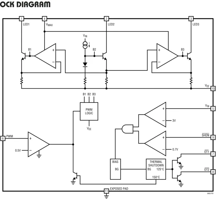
BLOCK DIAGRAM
Figure 1. Block Diagram
1 2 – + – + – + 4 VEE B1 B2 B3 LED1 PWM 0.5V VMAX LED2 11 EXPOSED PAD LED3 3 VIN 3V 5 VEE SHDN 0.7V 9 OT1 7 PWM LOGIC THERMAL SHUTDOWN BIAS BG BG 125°C 150°C OT2 3003 F01 8 6 – + 10 – + B2 B1 VIN B3 VEE (Pin 10): Lower Rail.
• Boost: Connect to System Ground • Buck Mode: Connect to Inductor
• Buck-Boost Mode: Connect to Input Supply
Exposed Pad (Pin 11): GND. The ground for the IC should be soldered to a continuous copper ground plane under the LT3003 die. Soldering the Exposed Pad to the copper ground plane under the device will reduce thermal resis-tance and increase the power capability of the LT3003.
PIN FUNCTIONS
6
3003fa The LT3003 is an easy-to-use 3-channel LED ballaster.
It allows three strings of LEDs to be driven in parallel with accurate LED current matching. A PWM pin is also provided allowing LED currents to be turned on and off at very low duty cycles for very wide LED dimming ranges. For reliable system thermal management, two output fl ags, OT1 and OT2, are provided to indicate when the junction temperature exceeds 125°C.
The Block Diagram in Figure 1 best illustrates the features of LT3003. The LT3003 internal bias circuitry is turned on when VIN > 3V and SHDN > 0.7V. For LED current to be active in each channel, the PWM pin must exceed 0.5V. VMAX should be connected to the highest supply in the application (see various application modes of boost, buck, buck-boost in the Typical Applications section).
The LT3003 ballasting feature is achieved by using the current monitored in the LED2 channel to control the current in channels LED1 and LED3. A servo loop exists for each channel LED1 and LED3 that compares the cur-rent in each channel to the LED2 reference channel. The current in LED2 channel is determined by the LED current programmed by the partner LED driver. Details of how LED current can be programmed by the partner IC are covered in the Typical Applications section using various ICs as LED drivers. Maximum fault current in each of the LT3003 LED pins is internally limited to 550mA. If any LED string experiences an open-circuit fault, all LED string currents are turned off.
The LT3003 PWM pin has unique level-shifting circuitry to allow a simple logic-level PWM signal to turn each LED pin current on and off regardless of the VEE pin voltage. This allows very simple PWM dimming control of LED current without any need for external level-shifting components in buck mode and buck-boost mode applications. Care is taken to ensure low current (nano amps) in the VEE and VMAX pins 10µs after PWM low edge. This feature mini-mizes leakage currents in each application to maximize PWM dimming ratio. Details of PWM dimming and criti-cal parameters are given in the Applications Information section PWM Dimming.
The LT3003 incorporates internal junction temperature sensing and provides two open-collector outputs, OT1 and OT2, which become active low when junction tem-perature exceeds 125°C. OT1 is sized to pull 100µA and can be used as an input to the microprocessor for system thermal management. OT2 is sized to pull 300µA to defeat switching for most of LTC’s LED drivers by pulling down the gm error amplifi er output. LT3003 is forced to a “zero LED current state” by a special internal protection circuit when junction temperature reaches 150°C.
To calculate the LT3003 junction temperature, see Thermal Calculations in the Applications Information section.
OPERATION
7
3003fa Input Capacitor Selection
The LT3003 is typically driven from the same input voltage used for the partner LED driver IC. The LED driver and inductor govern the requirements for the input capacitor of the application. A ceramic input capacitor in the range of 1µF to 10µF works for most applications. In cases where the LT3003 input voltage is derived separately from the LED driver, a 1µF input capacitor works well.
LED Current Matching
An LED driver programs the LED current and LT3003 ac-tively ballasts three separate strings of LEDs. The currents in all three channels will be matched to better than ±3%. To achieve best current matching, (VIN – VEE) should be between 3V and 10V. A low (VIN – VEE) also minimizes LT3003 internal power dissipation (see Thermal Calcula-tion secCalcula-tion for more informaCalcula-tion).
PWM Dimming
The LT3003 has a wide PWM dimming range for constant color LED dimming. PWM dimming is superior to analog dimming as it preserves true color quality. PWM dimming control with the LT3003 is achieved using a simple ground referenced PWM signal with a 0.5V on/off threshold. The LEDs operate at either programmed or zero current but their brightness changes with the PWM signal duty cycle. When PWM is low, LED strings are completely discon-nected. In addition, the LT3003 switches to low power standby mode ~10µs after PWM low edge, resulting in higher system power effi ciency.
For the widest dimming range, the PWM signal should be 100Hz. The human eye is typically sensitive to fl ickering below ~80Hz. Operating the PWM higher than 100Hz results in a reduced PWM dimming ratio.
Achieving high PWM dimming ratios require attention to circuit leakages, such as reverse bias leakage currents through the external Schottky. Hence, for high PWM dim-ming ratios, components should be chosen to minimize leakage currents.
If an application does not require PWM dimming, the PWM pin can be left open (unconnected) and an internal 10µA source current pulls PWM high.
Boost PWM Dimming
The LT3003 supports up to a 3000:1 PWM dimming ratio with a 100Hz PWM dimming frequency. To achieve such high PWM ratios, leakages of the LED driver and other external components should be minimal.
Buck Mode: PWM Dimming
The LT3003 supports up to a 3000:1 PWM dimming ratio in buck mode. The PWM dimming in buck mode is achieved by an architecture that allows the LT3003 power ground (VEE) to move with output capacitor voltage. PWM dim-ming control is achieved by a simple ground referenced PWM signal, eliminating the need for any external level-shift component.
High PWM dimming ratios require very low VEE and
VMAX pin currents during the PWM off state. The LT3003
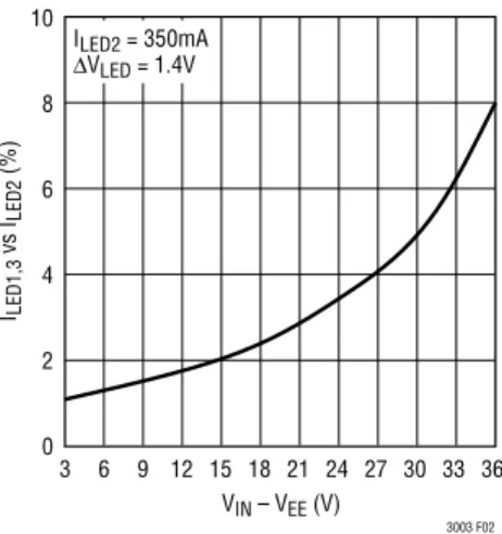
VIN – VEE (V) 3 ILED1,3 vs I LED2 (%) 8 12 3003 F02 2 6 9 0 10 6 4 36 33 30 27 24 21 18 15 ILED2 = 350mA ∆VLED = 1.4V
Figure 2. ILED Matching vs (VIN – VEE)
LED Pin Current Range
The steady-state operational current range for each LED pin is between 100mA and 350mA. Internal protection circuitry limits absolute maximum pin current to 550mA.
LED Open-Circuit Protection
If any LED string is open, then currents in all three chan-nels reduce to zero. The driver chip, which supplies LED current, should have an overvoltage clamp to protect the LT3003 from high LED pin voltages.
8
3003fa uses novel circuit techniques to reduce VEE and VMAX pin currents to nano amp range ~10µs after PWM low edge. This preserves the output capacitor voltage and results in higher PWM dimming ratios.
Buck-Boost Mode: PWM Dimming
The LT3003 can also perform PWM dimming in buck-boost mode. The buck-boost confi guration requires the PWM and SHDN pins to be tied together. This confi guration can support up to a 2000:1 PWM dimming ratio.
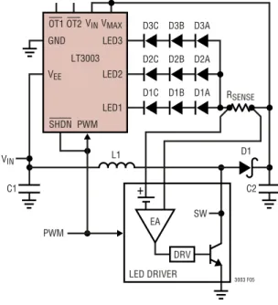
DRV LED DRIVER SW PWM L1 D1 C1 C2 VIN RSENSE
D1A D2A D3A D1B D2B D3B D1C D2C D3C + LED1 PWM SHDN VIN OT1 OT2 LED2 LT3003 LED3 VEE GND 3003 F03 VMAX EA
Figure 3. Boost Mode
DRV LED DRIVER SW C1 C2 D1 VIN RSENSE
D1A D2A D3A D1B D2B D3B D1C D2C D3C + LED1 PWM L1 PWM OT1 OT2 SHDN LED2 LT3003 LED3 VEE GND 3003 F04 VIN VMAX EA
Figure 4. Buck Mode
C1 C2 D3C D3B D3A 3003 F05 LED3 D2C D2B D2A LED2 GND VEE VIN D1C D1B D1A LED1 OT1 OT2 SHDN PWM PWM VINVMAX LT3003 DRV LED DRIVER SW + EA L1 D1 RSENSE
Figure 5. Buck-Boost Mode
Overtemperature Protection
The LT3003 incorporates internal junction temperature sensing and provides two open-collector outputs, OT1 and OT2, which become active low when junction temperature exceeds 125°C. The active OT1 output can sink 100µA of current and can be connected to system microprocessor. The active low OT2 output can sink 300µA of current and can be connected to the switching regulator’s gm error amplifi er output to defeat switching. The LT3003 has to cool down by 6°C (119°C) for OT1 and OT2 outputs to reset (collector outputs high).
9
3003fa In addition, LT3003 has an internal 150°C overtemperature
protection circuitry that resets the chip to zero LED current mode. This prevents the chip from continuous operation at high temperature.
Thermal Calculations
To maximize output power capability in an application without exceeding the LT3003 125°C maximum operational junction temperature, it is useful to be able to calculate power dissipation within the IC. The power dissipation within the LT3003 comes from four main sources: switch DC loss, switch loss due to LED VLED mismatch and input quiescent current.
1. Switch DC Loss:
PSW(DC) = ILED • VLED • 3
(See (VLED1,2,3 – VEE) vs ILED Typical Performance Characteristics graph.)
2. Switch Loss due to VLED Mismatch: PSW(ΔVLED) = Total VLED mismatch • ILED 3. Input Quiescent Loss:
PQ = (VIN – VEE) • (IQ – 1mA) + 1mA • VIN
IQ =3 ILED + mA
40 3
•
4. Total Power Dissipation:
PTOT = PSW(DC) + PSW(ΔVLED) + PQ 5. LT3003 Junction Temperature: TJ (LT3003) = TA + θJA(PTOT); θJA(PTOT) = PTOT • 35°C/W Example VIN = 3V; VEE = 0V; ILED = 350mA/string; • IQ =3 350mA+ mA= mA 40 3 29 25 • . Total VLED mismatch = 1V:
• e.g., LED string 1 voltage drop = 6V; LED string 2 voltage drop = 5.7V; LED string 3 voltage drop = 5.3V
• Total VLED mismatch = (6V – 5.7V) + (6V – 5.3V) = 1V VLED = 1.1V at ILED = 350mA (see (VLED – VEE) vs ILED Typical Performance Characteristics graph).
1. PSW(DC) = 3 • 350mA • (1.1V) = 1.16W 2. PSW(LED) = 1000mV • 350mA = 350mW
3. PQ = (3 – 0) • (29.25 – 1)mA + 3 • 1mA = 88mW
4. PTOT = 1.1W + 350mW + 88mW ≈1.6W
The LT3003 uses a thermally enhanced 10-lead MSE package. With proper soldering of the Exposed Pad to the underside of the package, combined with a full copper plane underneath the device, the thermal resistance (θJA)
is about 35°C/W. For an ambient temperature of TA = 25°C, the junction temperature of the LT3003, for the example application described above, can be calculated as: 5. TJ = TA + θJA • PTOT = 25°C + 35°C/W • 1.6W
= 81°C
Minimizing LT3003 Internal Power Dissipation
The LT3003 requires at least 3V headroom between VIN and VEE. Hence, for systems with high system input volt-age and low VEE (such as running multiple series LEDs in a Buck Mode), it is benefi cial to lower the level of VIN pin voltage (LT3003 upper rail) with an external zener to reduce power dissipation in the chip. Therefore, it is recom-mended to limit (VIN – VEE) to less than 10V. To achieve best performance, (VIN – VEE) should equal 3V.
10
3003fa 1.05A Buck Mode LT3003 with the LT3476
LED LED LED LED R1 0.1Ω LED LED 1 2 9 5 4 10 C2 0.33µF 1nF C1 1µF R3 21k 4.7µF 35V 1µF PVIN 32V VIN 3V TO 16V L1 10µH D1 D2 20V 3 6 3003 TA02a OT1 7 OT2 LT3003 VIN VMAX 8 GND 11 LED1 LED2 LED3 8 LEDs PER STRING; 350mA PER STRING
C1: TDK C1608X7R1C105K
C2: TAIYO YUDEN GMK212BJ334MG-T D1: DIODES INC. DFLS140
L1: TOKO A916CY-100M-P3 LED: LUMILEDS LUXEON
SHDN VEE PWM CAP1 VIN SHDN LT3476 GND NC 3 18 33 2 7 37 6 LED1 REF VADJ1 35 PWM1 29 SW1 RT 28 39 SW1 1 VC1 19-21, 30-32
TOTAL LED CURRENT (mA) 0 60 EFFICIENCY (%) 65 70 75 80 90 200 400 600 800 3003 TA02b 1000 1200 85 PVIN = 33V NUMBER OF LEDS = 8 × 3 = 24 Effi ciency
TYPICAL APPLICATIONS
11
3003fa 330mA Boost LT3003 with the LT3477
LT3003 VIN VIN C3 1µF 25V 3003 TA03a ILED
110mA PER STRING 6 to 8
LEDs PER STRING
4 5 9 11 10 VMAX PWM 8 7 6 6 13 14 16 17 D1 11 3 2 1 VOUT 4V LED1 LED2 LED3
VEE GND SHDN OT1 OT2 FBN ISP2 3 7 8 5 12 2 4 21 15 PWM R3 6.81k ISN2 FBP VREF RT VC D2 1N4148W SHDN LT3477 ISP1 ISN1 SW SW GND GND SS NC NC NC 1 10 9 VIN IADJ1 IADJ2 18 19 20 R4 0.3Ω 1% R5 1.15M 1% L1 4.7µH VIN 8V TO 16V R6 45.3k 1% C3 0.033µF C4 4.7µF 50V VOUT C2 22nF C1, C3: TAIYO YUDEN TMK212BJ105MG-BR C4: MURATA GRM32ER71H475KA88L D1: DIODES INC. DFLS140 L1: SUMIDA CDRH5D16-4R7 Q1 2N7002 C1 1µF 25V PWM DIMMING RATIO 1 TOTAL I LED (mA) 10 100 10000 3003 TA03b 1 0.1 10 100 1000 1000
ILED = 110mA PER STRING
NUMBER OF LEDS = 8 × 3 = 24 VIN (V) 8 50 EFFICIENCY (%) 55 65 70 75 100 85 10 12 13 3003 TA03b 60 90 95 80 9 11 14 15 16
ILED = 110mA PER STRING
NUMBER OF LEDS = 8 × 3 = 24
PWM Dimming Effi ciency
12
3003fa 300mA Buck-Boost Mode LT3003 with the LT3477
LT3003 VIN 1 2 3 6 9 8 7 VMAX PWM 7 6 D1 4 5 D3 LED1 LED1 LED2 LED3 VEE GND
SHDN OT2 OT1 LED2 LED3 ILED = 100mA
LED4 LED5 LED6 LED7 LED8 LED9 LED10 LED11 LED12
FBN SHDN SS VC LT3477 ISP1 ISN1 SW GND FBP VREF ISP2 ISN2 RT VIN IADJ1 IADJ2 10µH R0.33SENSEΩ 3.3µF 50V CER D1: ZETEX ZLLS1000 D2: DIODES INC 1N4148 D3: PHILIPS PDZ9.1B NMOS: ZETEX 2N7002 NMOS D2 PWM 3003 TA04a 280k 10k 10nF 33nF CER VIN 8V TO 16V 33µF CER 1µF 0V 5V 100Hz 6.81k Effi ciency VIN (V) 6 68 EFFICIENCY (%) 70 72 74 76 80 8 10 12 14 3003 TA04b 16 18 78 ILED = 200mA ILED = 100mA NUMBER OF LEDS = 4 × 3 = 12
TYPICAL APPLICATIONS
13
3003fa 1A Buck Mode LT3003 with the LT1618
Effi ciency LT3003 LED2 LED3 LED1 D1 14V R1 1M VIN 5V C3 1µF 50V L1 10µH 1.5A PWM 100Hz, 5V 500:1 MAX PWM DIMMING RATIO COUT 1µF 50V CER 220pF GND PWM VMAX ILED = 333mA PER STRING VEE VIN SHDN OT1 OT2 C1 4.7µF 50V CER 10nF 3003 TA05a 1k 1N4148W ZLLS1000 RSENSE 0.05Ω 1%, 1A ISN LT1618 ISP VIN SHDN SW Q4 2N7002 VC IADJ GND FB NC 1µF 10V CER VIN 32V
TOTAL LED CURRENT (A) 0 77 EFFICIENCY (%) 78 79 80 81 82 83 0.2 0.4 0.6 0.8 3003 TA05b 1.0 NUMBER OF LEDS = 6 × 3 = 18
TYPICAL APPLICATIONS
14
3003fa 1A Buck LT3003 with the LT3475
Effi ciency LT3003 GND 20V LED1 LED2 LED3 VMAX VIN VEE SHDN OT2 OT1 PWM PWM1 100Hz 2000:1 MAX PWM DIMMING RATIO LED1 LED4 LED7 LED2
330mA PER STRING 3S 3P LUXEON I WHITE LED5 LED8 LED3 LED6 LED9 C3 1µF 50V VIN 5 6 16 11 20 8 10 7 3 1 4 R1 20k VIN SHDN PWM1 PWM2 BOOST1 OUT1 17 REF SW1 LED1 D1 1N4448W D2 B240A C1 0.22µF X5R R4 1.0k L1 10µH SUMIDA BOOST2 OUT2 SW2 9 2 GND RT GND LT3475 LED2 SECOND CHANNEL ONE OF TWO CHANNELS SHOWN R8 2.0k 19 12 VADJ1 VADJ2 R10 10k R12 11.8k 1% R13 1.0M C7 220pF Q3 2N7002 C5 0.1µF C3 3300pF COUT1 2.2µF 16V CIN1 4.7µF 50V 13 15 14 21 fSW = 1MHz 3003 TA06a 18 VC1 VC2 VIN 24V
TOTAL LED CURRENT (A) 0 50 EFFICIENCY (%) 65 70 80 0.2 0.4 0.6 0.8 3003 TA06b 1.0 90 100 55 65 75 85 95 1.2
TYPICAL APPLICATIONS
15
3003fa Information furnished by Linear Technology Corporation is believed to be accurate and reliable.
However, no responsibility is assumed for its use. Linear Technology Corporation makes no represen-tation that the interconnection of its circuits as described herein will not infringe on existing patent rights.
MSE Package 10-Lead Plastic MSOP
(Reference LTC DWG # 05-08-1664) MSOP (MSE) 0603 0.53 ± 0.152 (.021 ± .006) SEATING PLANE 0.18 (.007) 1.10 (.043) MAX 0.17 – 0.27 (.007 – .011) TYP 0.86 (.034) REF 0.50 (.0197) BSC 1 2 3 4 5 4.90 ± 0.152 (.193 ± .006) 0.497 ± 0.076 (.0196 ± .003) REF 8 9 10 10 1 7 6 3.00 ± 0.102 (.118 ± .004) (NOTE 3) 3.00 ± 0.102 (.118 ± .004) (NOTE 4) NOTE: 1. DIMENSIONS IN MILLIMETER/(INCH) 2. DRAWING NOT TO SCALE
3. DIMENSION DOES NOT INCLUDE MOLD FLASH, PROTRUSIONS OR GATE BURRS.
MOLD FLASH, PROTRUSIONS OR GATE BURRS SHALL NOT EXCEED 0.152mm (.006") PER SIDE 4. DIMENSION DOES NOT INCLUDE INTERLEAD FLASH OR PROTRUSIONS.
INTERLEAD FLASH OR PROTRUSIONS SHALL NOT EXCEED 0.152mm (.006") PER SIDE 5. LEAD COPLANARITY (BOTTOM OF LEADS AFTER FORMING) SHALL BE 0.102mm (.004") MAX
0.254 (.010) 0° – 6° TYP DETAIL “A” DETAIL “A” GAUGE PLANE 5.23 (.206) MIN 3.20 – 3.45 (.126 – .136) 0.889 ± 0.127 (.035 ± .005)
RECOMMENDED SOLDER PAD LAYOUT
0.305 ± 0.038 (.0120 ± .0015) TYP 2.083 ± 0.102 (.082 ± .004) 2.794 ± 0.102 (.110 ± .004) 0.50 (.0197) BSC BOTTOM VIEW OF EXPOSED PAD OPTION
1.83 ± 0.102 (.072 ± .004) 2.06 ± 0.102 (.081 ± .004) 0.127 ± 0.076 (.005 ± .003)
PACKAGE DESCRIPTION
16
3003fa
Linear Technology Corporation
1630 McCarthy Blvd., Milpitas, CA 95035-7417
(408) 432-1900 ● FAX: (408) 434-0507 ● www.linear.com © LINEAR TECHNOLOGY CORPORATION 2006
LT 0107 REV A • PRINTED IN USA
PART NUMBER DESCRIPTION COMMENTS
LT1618 Constant-Current/Constant-Voltage DC/DC Converter Drives 20 White LEDs from Li-Ion, 10-Lead MS Package
LT1932 Constant Current,1.2MHz, High Effi ciency White LED Boost
Regulator
VIN: 1V to 10V, VOUT(MAX) = 34V, IQ = 1.2mA, ISD < 1µA, ThinSOTTM
Package
LT1942 Quad DC/DC Converter for Triple Output TFT Supply Plus Boost
LED Driver, with a 2-Channel Ballaster
TFT Supply: Three Switching Regulators (Two Boost, One Inverting)
LED Supply: Up to Two Strings of 10 LEDs. VIN: 2.6V to 16V,
VOUT(MAX) = 45V, IQ = 7mA, ISD < 1µA, Low Profi le QFN package.
LT3475 36V, 2MHz, Dual 1.5A Step-Down LED Driver VIN: 4V to 36V, 200kHz to 2MHz, TSSOP20E Package, 3000:1
Dimming
LT3477 3A, 3.5mHz, Constant-Current DC/DC Converter with Dual
Rail Sense. Can Drive LEDs in Boost, Buck and Buck-Boost Confi gurations
VIN: 2.5V to 25V, VOUT(MAX) = 42V, ISD < 1µA, QFN/TSSOP Packages
LT3478 4.5A Constant Current BOOST LED Driver with PWM VIN: 2.7V to 36V, VOUT(MAX) = 40V, ILED(MAX) = 1.05A, ISD < 5µA,
FE16 Package
LT3479 3A, 3.5MHz, 42V Full Featured Boost/Inverter Converter with
Soft-Start
VIN: 2.5V to 24V, VOUT(MAX) = 40V, IQ = 5mA, ISD < 1µA, DFN/TSSOP
Packages
LT3474 36V, 2MHz, Step-Down 1A LED Driver VIN: 4V to 36V, 200kHz to 2MHz, TSSOP16E Package, 400:1
Dimming
LTC3205 Multi-Display LED Controller, Step-Up/Step-Down Fractional
Charge Pump, Independent Current and Dimming Control
VIN: 2.8V to 4.5V, 800MHz, QFN Package
LTC3783 PWM LED Power and Boost, Flyback and SEPIC Controller VIN: 3.6V to 36V, 300kHz, DFN, TSSOP16E Package, 3000:1
Dimming ThinSOT is a trademark of Linear Technology Corporation.