Volume 4, Issue 1, January 2015
Optical Signal Processing Through Efficient
Electro Optic Modulators in Advanced Optical
Communication Networks Under Thermo-optic
Effects
Ahmed Nabih Zaki Rashed1*, Abd El-Naser A. Mohammed2 and Fatma Mohammed Aref Mahmoud Houssien3
1,2,3Electronics and Electrical Communications Engineering Department
Faculty of Electronic Engineering, Menouf 32951, Menoufia University, EGYPT
*E-mail: [email protected]
Abstract— Semiconductor optical modulator devices plays an important role in several rapidly developing areas of broadband communications, such as optical networking, metropolitan/access communications and computing systems due to their easier processibility and integration over inorganic counterparts. Optical telecommunication systems at high data rate require external modulation. An electro-optic modulator (EOM) is used for modulating the intensity of the laser beam according to the logical levels of the digital data. This paper has presented the important transmission characteristics, operation efficiency, and modulation speed performance design parameters of different electro-optic polymer modulators. The switching voltage, figure of merit, extinction ratio, modulation, transit time, modulator performance speed, and DC half wavelength length product are the major important design parameters of our interesting. As well as we have investigated semiconductor electro-optic modulators such as silicon (Si), gallium arsenide (GaAs), and indium phosphoide (InP) under thermo-optic effects over wide range of the affecting parameters for integrated photonics applications. Optical interconnect technology is expected as a key solution to solving major performance limitations in high performance computing caused by bus bandwidth bottleneck, latency and power consumption issues. Our results are validated against published experimental work and showed good agreement and enhancement.
Index Terms— Integrated photonics, Thermo-Optic, Broadband communications, and Mach-Zehnder (MZ) modulator.
I.INTRODUCTION
Over the past few years, the demands for high performance computers, ever increasing instructions per cycle and high energy efficiency, have fuelled the rapid development of multicore and many core microprocessors. With the recent advent of quad core processors into the market [1], coupled with the laboratory demonstration of a teraflop processor containing 80 cores, the need for interconnects supporting gigascale and terascale input/output has become imperative. Although present implementations of chip to chip copper interconnects are being pushed to deliver gigascale bandwidths with the design of transceivers that use active or passive equalizers, this is unlikely to be a frequency scalable option. On a parallel front, optical technology has been successfully deployed in long haul fiber communications for more than two decades now. Individual components targeted toward these applications have been developed to the extent of delivering bandwidths as large as 40 Gb/s. Multiple
wavelength division multiplexing (WDM) is capable of terascale data rates [2].
It would therefore seem intuitive to extensively employ similar optical technology in short reach applications such as rack to rack and board to board communications. However, this approach has not gathered momentum and the primary reason has been the high costs of materials such as III-V semiconductors and lithium niobate, which are inherently suited for photonic applications. Thus, developing a cost-effective optical technology has become essential for its adoption in the computer industry. Interest in silicon photonics has been spurred predominantly by the low cost of silicon. In addition, its high volume manufacturability and the potential of electronics and photonics integration in the all pervasive microelectronics applications have added a further boost to this field. Silicon photonics is now being enabled by the successful demonstration of the requisite building blocks on silicon such as fast silicon optical modulators [3], SiGe photodetectors [4], silicon Raman lasers [5], silicon optical amplifiers [6], silicon wavelength converters [7], and hybrid silicon lasers. A high speed silicon photonic transceiver circuit which monolithically integrates all of these functionalities would be the ultimate culmination point expected to provide a low-cost solution for future optical interconnects. Silicon optical modulators are one of the key building blocks which have been extensively studied. High-speed data transmission at 10 Gb/s [8], 30 Gb/s [9], and 40 Gb/s [10] has been demonstrated using silicon modulators with different device configurations. Combining these gigascale silicon modulators with recently developed hybrid silicon lasers [11] and using WDM, one could create a single chip that can transmit data at Tb/s data rate for future high performance computing applications and mega data centers.
II.SIMPLE OPTICAL COMMUNICATION LINK WITH MZ MODULATOR
Fig. 1. Schematic view of optical communication link with MZ modulator.
It can be readily seen that optical modulators are a key component in an optical communications link. There are several commercially techniques to modulate a laser source: direct laser modulation, and electro-optic modulator with electrode modulation length L, and spacing between electrodes d are all currently commercially available. Each type of modulation has unique benefits and limitations [12].
III.MATHEMATICAL MODEL ANALYSIS
The thermo-optic effect is present in all transparent materials and describes the dependence of the material index of refraction on temperature. Mathematically, this can be expressed in the following form [13-16]:
T dT n
n e e (1)
Where dne/dT is the thermo-optic coefficient, ΔT=(T-T0) is
the difference between ambient temperature (T), and room temperature (T0), and ne is the effective refractive index of
the material based thermal EO intensity modulator is given by the following formula:
2 , 6 2 2 5 2 4 2 2 3 2 2 2 2 1 A A A A A A ne (2)
2 2 6 2 6 6 5 2 2 4 2 4 4 3 2 2 2 2 2 2 1 2 A T A A A A T A A A A T A A A n dT dn e e (3)
The set of parameters of empirical equation coefficients for different polymeric materials based EO intensity modulators are recast and dimensionally as listed in Table 1 as a function of ambient temperature T, and room temperature T0. The set of different polymeric materials based EO
modulators and their electro-optic and absorption coefficients at third optical transmission window (at λ=1.55 μm)are listed in Table 1 [17, 18].
Table 1: Electro-optic and absorption coefficients for semiconductor materials at 3rd optical transmission window [12, 17, 19, 22].
Coefficients Materials based EO modulators
Silicon (Si) Gallium Arsenide (GaAs) Indium Phosphide (InP)
A1 1.0668429 (T/T0) 4.08765 (T/T0) 1.2876532 (T/T0)
A2 0.301516485 (T/T0)2 0.2088764 (T/T0)2 0.1197543 (T/T0)2
A3 0.0030434748 (T/T0) 0.7432544 (T/T0) 0.77432987 (T/T0)
A4 1.13475115 (T/T0)2 0.3956432 (T/T0)2 0.36541232 (T/T0)2
A5 1.5413308 (T/T0) 0.9887654 (T/T0) 2.9876521 (T/T0)
A6 1104 (T/T0)2 27.654387 (T/T0)2 153.75232 (T/T0)2
Electro-optic coefficient (r41) 15 Pm/volt 1.43 Pm/Volt 5.8 Pm/Volt
Material absorption coefficient (α) 0.1 dB/cm 0.5 dB/cm 3 dB/cm
The thermo-optic effect in silicon is large and as such can be used to impart large variations in refractive index with modest increases in material temperature. When such a change occurs uniformly over a finite length, L, then the change in optical phase relative to unperturbed propagation is given by [19, 20]:
dT dn T L
2 , (4)
Where L is the length of the modulation electrode and T is the temperature rise over this length. When this phase term is applied to a symmetrical two beam, the resulting modulated output current as a function of bias current is given by:
cos 1 500 0 IbiasI (5)
Based on MATLAB curve fitting program, the fitting relation between bias current (Ibias) in mA and applied bias
voltage (Vbias) in Volts can be given by [21]: 2 0564 . 0 743 . 0 546 .
0 bias bias
bias V V
I (6)
Where Vπ is the voltage required to change the output light
intensity from its maximum value to its minimum value can be:
, 2 n3 r41L
d V
(7)
Where d is the distance between the top and the bottom electrodes, L is the length of the modulation electrode, λ is the operating optical signal wavelength, r41 is the
electro-optic coefficient, and Г is confinement factor, and is defined as the overlap integration of the modulating electrical field and the optical mode. The change in effective refractive index for the transverse magnetic polarization is [22]:
, 5
.
0 3 41
L r n V n bias
(8)
The thermal sensitivity of EOM under thermo-optic effect can be given by [23]:
, dT dn n T
SM K-1 (9)
Volume 4, Issue 1, January 2015
, 10 0.1
V
FoM (10)
Where α is the material absorption coefficient, and Vπ is the
switching voltage for 100% modulation at the operating frequency. This figure of merit expresses the amount of modulated optical power that can be made available at the output of a modulator, for a certain amount of radio frequency drive power [26]. Therefore, the higher the FoM, the higher the gain and the better. Also based on MATLAB curve fitting program, the fitting relations between the extinction ratio (ER), modulation efficiency (ηm) against Vπ
can be given by:
, 19349 . 0
20 V V2
ER (11)
, 8182 . 0 163 . 4 4 .
46 2
m V V (12)
Where the root mean square errors for the previous fitting equations are 0.00598%, 0.003785% respectively. The transit time of EO polymeric modulators is given by [27]:
, c n
L
d
nsec (13)
To obtain a high modulation speed, the transit time should be as small as possible. The 3-dB bandwidth which is a guide of device operation efficiency can be expressed as [23, 27, 28]:
L c n
f3dB2 , GHz (14)
The transmission modulation bit rate length product can be described by [22]:
, L B
PR Rm Gbit.cm/sec (15)
Where the modulation bit rate with non return to zero coding can be expressed by the following expression [29]:
d Rm B
7 . 0
Gbit/sec (16)
IV.SIMULATION RESULTS AND PERFORMANCE EVALUATION
We have investigated the development of different semiconductor electro-optic modulators for high speed performance operation in optical communication networks over wide range of the affecting operating parameters as shown in Table 2.
Table 2: Proposed operating parameters for different semiconductor EOMs [3, 5, 7, 12, 15].
Operating parameter Symbol Value
Operating signal wavelength λ 1.55 μm Electrode modulator length L 1 ≤ L, cm ≤ 2 Distance between electrodes d 10 ≤ d, µm ≤ 50 Bias voltage Vbias 1 ≤ Vbiass, Volt ≤ 10
Confinement factor Г 0.9
Room temperature T0 300 K
Ambient temperature T 300 K-350 K
Based on the modeling equations analysis over wide range of the operating parameters, and the series of the Figs. (2-26), the following features are assured:
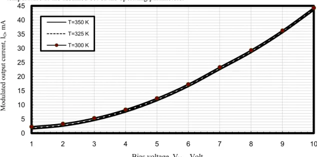
i) Figs. (2-4) have indicated that modulated output current increases for different electro-optic modulators under study with increasing both ambient temperature variations and applied bias voltage. It is found that silicon electro-optic modulator has presented the highest modulated output current in compared with other modulators.
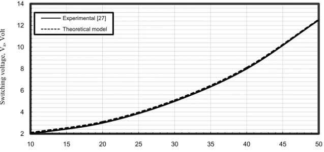
ii) As shown in Figs. (5-7) have demonstrated that switching voltage increases with increasing distance between electrodes for different electro-optic modulators under study. As well as it is evident that silicon electro-optic modulator has presented the lowest switching voltage in compared with other modulators. iii) Figs. (8-10) have indicated that modulator thermal
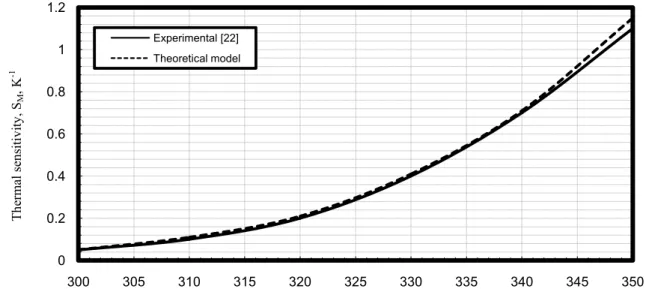
sensitivity increases with increasing ambient temperature variations for different electro-optic modulators under study. As well as it is indicated that indium phosphide electro-optic modulator has presented the lowest thermal sensitivity in compared with other modulators.
iv) Figs. (11-13) have assured that figure of merit increases for different electro-optic modulators under study with increasing electrode modulator length and decreasing ambient temperature variations. As well as it is evident that silicon electro-optic modulator has presented the highest figure of merit in compared with other modulators.
Bias voltage, Vbias, Volt
Fig. 2. Variations of modulated output current for silicon modulator against variations of bias voltage and ambient temperature at the assumed set of the operating parameters.
Bias voltage, Vbias, Volt
Fig. 3. Variations of modulated output current for gallium arsenide modulator against variations of bias voltage and ambient temperature at the assumed set of the operating parameters.
Bias voltage, Vbias, Volt
Fig. 4. Variations of modulated output current for indium phosphide modulator against variations of bias voltage and ambient temperature at the assumed set of the operating parameters.
0 10 20 30 40 50 60
1 2 3 4 5 6 7 8 9 10
T=350 K
T=325 K
T=300 K
0 10 20 30 40 50 60
1 2 3 4 5 6 7 8 9 10
T=350 K
T=325 K
T=300 K
0 5 10 15 20 25 30 35 40 45
1 2 3 4 5 6 7 8 9 10
T=350 K
T=325 K
T=300 K
M
od
ulate
d
ou
tp
ut
cu
rre
nt,
IO
, m
A
M
od
ulate
d
ou
tp
ut
cu
rre
nt,
IO
, m
A
M
od
ulate
d
ou
tp
ut
cu
rre
nt,
IO
, m
Volume 4, Issue 1, January 2015
Distance between electrodes, d, μm
Fig. 5. Switching voltage in relation to distance between electrodes with electrode modulator length (L=1.5 cm) for silicon modulator at the assumed set of the operating parameters.
Distance between electrodes, d, μm
Fig. 6. Switching voltage in relation to distance between electrodes with electrode modulator length (L=1.5 cm) for gallium arsenide modulator at the assumed set of the operating parameters.
Distance between electrodes, d, μm
Fig. 7. Switching voltage in relation to distance between electrodes with electrode modulator length (L=1.5 cm) for indium phosphide modulator at the assumed set of the operating parameters.
0.2 0.4 0.6 0.8 1 1.2 1.4
10 15 20 25 30 35 40 45 50
Experimental [18]
Theoretical model
2 4 6 8 10 12 14
10 15 20 25 30 35 40 45 50
Experimental [27]
Theoretical model
0.5 1 1.5 2 2.5 3 3.5
10 15 20 25 30 35 40 45 50
Experimental [22]
Theoretical model
S
witch
in
g
vo
lt
ag
e,
Vπ
, V
olt
S
witch
in
g
vo
lt
ag
e,
Vπ
, V
olt
S
witch
in
g
vo
lt
ag
e,
Vπ
, V
Ambient temperature, T, K
Fig. 8. Variations of silicon modulator thermal sensitivity against variations of ambient temperature at the assumed set of the operating parameters.
Ambient temperature, T, K
Fig. 9. Variations of gallium arsenide modulator thermal sensitivity against variations of ambient temperature at the assumed set of the operating parameters.
Ambient temperature, T, K
Fig. 10. Variations of indium phosphide modulator thermal sensitivity against variations of ambient temperature at the assumed set of the operating parameters.
0.4 0.6 0.8 1 1.2 1.4 1.6 1.8
300 305 310 315 320 325 330 335 340 345 350
Experimental [18]
Theoretical model
0.5 1 1.5 2 2.5 3
300 305 310 315 320 325 330 335 340 345 350
Experimental [27]
Theoretical model
0 0.2 0.4 0.6 0.8 1 1.2
300 305 310 315 320 325 330 335 340 345 350
Experimental [22] Theoretical model
Th
erm
al
se
nsiti
vi
ty
, SM
, K
-1
Th
erm
al
se
nsiti
vi
ty
, SM
, K
-1
Th
erm
al
se
nsiti
vi
ty
, S
M
, K
Volume 4, Issue 1, January 2015
Electrode modulator length, L, cm
Fig. 11. Figure of merit of silicon modulator in relation to electrode modulator length and ambient temperatures at the assumed set of the operating parameters.
Electrode modulator length, L, cm
Fig. 12. Figure of merit of gallium arsenide modulator in relation to electrode modulator length and ambient temperatures at the assumed set of the operating parameters.
Electrode modulator length, L, cm
Fig. 13. Figure of merit of indium phosphide modulator in relation to electrode modulator length and ambient temperatures at the assumed set of the operating parameters.
0 0.1 0.2 0.3 0.4 0.5 0.6 0.7 0.8 0.9
1 1.1 1.2 1.3 1.4 1.5 1.6 1.7 1.8 1.9 2
T=300 K
T=325 K
T=350 K
0 0.1 0.2 0.3 0.4 0.5 0.6
1 1.1 1.2 1.3 1.4 1.5 1.6 1.7 1.8 1.9 2
T=300 K
T=325 K
T=350 K
0 0.05 0.1 0.15 0.2 0.25 0.3 0.35 0.4 0.45
1 1.1 1.2 1.3 1.4 1.5 1.6 1.7 1.8 1.9 2
T=300 K
T=325 K
T=350 K
F
ig
ure
o
f
m
erit
, F
oM
, V
-1 .c
m
-1
F
ig
ure
o
f
m
erit
, F
oM
, V
-1 .c
m
-1
F
ig
ure
o
f
m
erit
, F
oM
, V
-1 .c
m
Distance between electrodes, d, μm
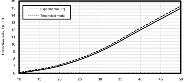
Fig. 14. Extinction ratio in relation to distance between electrodes with electrode modulator length (L=1.5 cm) for silicon modulator at the assumed set of the operating parameters.
Distance between electrodes, d, μm
Fig. 15. Extinction ratio in relation to distance between electrodes with electrode modulator length (L=1.5 cm) for gallium arsenide modulator at the assumed set of the operating parameters.
Distance between electrodes, d, μm
Fig. 16. Extinction ratio in relation to distance between electrodes with electrode modulator length (L=1.5 cm) for indium phosphide modulator at the assumed set of the operating parameters.
9 10 11 12 13 14 15 16 17 18 19
10 15 20 25 30 35 40 45 50
Experimental [18]
Theoretical model
6 7 8 9 10 11 12 13 14 15 16
10 15 20 25 30 35 40 45 50
Experimental [27]
Theoretical model
4 5 6 7 8 9 10 11 12 13
10 15 20 25 30 35 40 45 50
Experimental [22]
Theoretical model
Ex
tin
cti
on
ra
tio
, ER,
d
B
Ex
tin
cti
on
ra
tio
, ER,
d
B
Ex
tin
cti
on
ra
tio
, ER,
d
Volume 4, Issue 1, January 2015
Distance between electrodes, d, μm
Fig. 17. Modulation efficiency in relation to distance between electrodes with electrode modulator length (L=1.5 cm) for silicon modulator at the assumed set of the operating parameters.
Distance between electrodes, d, μm
Fig. 18. Modulation efficiency in relation to distance between electrodes with electrode modulator length (L=1.5 cm) for gallium arsenide modulator at the assumed set of the operating parameters.
Distance between electrodes, d, μm
Fig. 19. Modulation efficiency in relation to distance between electrodes with electrode modulator length (L=1.5 cm) for indium phosphide modulator at the assumed set of the operating parameters.
55 57.5 60 62.5 65 67.5 70 72.5
10 15 20 25 30 35 40 45 50
Experimental [18]
Theoretical model
45 47.5 50 52.5 55 57.5 60 62.5 65
10 15 20 25 30 35 40 45 50
Experimental [27]
Theoretical model
35 37.5 40 42.5 45 47.5 50 52.5 55 57.5
10 15 20 25 30 35 40 45 50
Experimental [22]
Theoretical model
M
od
ulati
on
e
fficie
nc
y,
ηm
, %
M
od
ulati
on
e
fficie
nc
y,
ηm
, %
M
od
ulati
on
e
fficie
nc
y,
ηm
, %
Electrode modulator length, L, cm
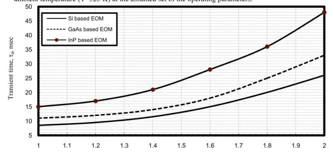
Fig. 20. Variations of transient time for different elect-optic modulators under study versus electrode modulator length with room temperature (T0=300 K) at the assumed set of the operating parameters.
Electrode modulator length, L, cm
Fig. 21. Variations of transient time for different elect-optic modulators under study versus electrode modulator length with ambient temperature (T=325 K) at the assumed set of the operating parameters.
Electrode modulator length, L, cm
Fig. 22. Variations of transient time for different elect-optic modulators under study versus electrode modulator length with ambient temperature (T=350 K) at the assumed set of the operating parameters.
5 10 15 20 25
1 1.1 1.2 1.3 1.4 1.5 1.6 1.7 1.8 1.9 2
Si based EOM GaAs based EOM
InP based EOM
5 10 15 20 25 30 35 40
1 1.1 1.2 1.3 1.4 1.5 1.6 1.7 1.8 1.9 2
Si based EOM
GaAs based EOM
InP based EOM
5 10 15 20 25 30 35 40 45 50
1 1.1 1.2 1.3 1.4 1.5 1.6 1.7 1.8 1.9 2
Si based EOM
GaAs based EOM
InP based EOM
Tran
sie
nt
ti
m
e,
τd
, n
se
c
Tran
sie
nt
ti
m
e,
τd
, n
se
c
Tran
sie
nt
ti
m
e,
τd
, n
se
Volume 4, Issue 1, January 2015
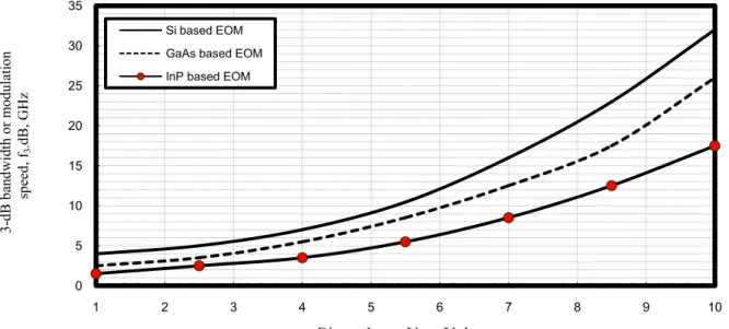
Bias voltage, Vbias, Volt
Fig. 23. Variations of modulation speed for different elect-optic modulators under study versus bias voltage with room temperature (T0=300 K) at the assumed set of the operating parameters.
Bias voltage, Vbias, Volt
Fig. 24. Variations of modulation speed for different elect-optic modulators under study versus bias voltage with ambient temperature (T=325 K) at the assumed set of the operating parameters.
Bias voltage, Vbias, Volt
Fig. 25. Variations of modulation speed for different elect-optic modulators under study versus bias voltage with ambient temperature (T=350 K) at the assumed set of the operating parameters.
0 5 10 15 20 25 30 35 40 45 50
1 2 3 4 5 6 7 8 9 10
Si based EOM
GaAs based EOM
InP based EOM
0 5 10 15 20 25 30 35
1 2 3 4 5 6 7 8 9 10
Si based EOM
GaAs based EOM
InP based EOM
0 5 10 15 20 25 30
1 2 3 4 5 6 7 8 9 10
Si based EOM
GaAs based EOM InP based EOM
3
-d
B
ba
nd
wid
th
o
r
m
od
ulati
on
sp
ee
d,
f
3-dB,
GH
z
3
-dB
b
an
dwid
th
o
r
m
od
ulati
on
sp
ee
d,
f
3-dB,
GH
z
3
-d
B
ba
nd
wid
th
o
r
m
od
ulati
on
sp
ee
d,
f
3-dB,
GH
Ambient temperature, T, K
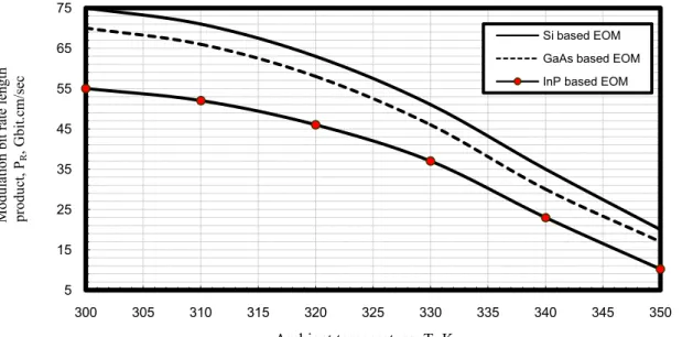
Fig. 26. Modulation bit rate length product for different electro-optic modulators in relation to ambient temperature variations at the assumed set of the operating parameters.
vi) Figs. (20-22) have assured that modulator transient time increases with increasing both electrode modulator length and ambient temperature variations for different electro-optic modulators under study. As well as it is evident that silicon electro-optic modulator has presented the lowest transient time in compared with other modulators.
vii) As shown in Figs. (23-25) have demonstrated that modulation operation speed increases with increasing applied bias voltage and decreasing ambient temperature variations for different electro-optic modulators under study. As well as it is indicated that silicon electro-optic modulator has presented the highest modulation operation speed in compared with other modulators.
viii) Fig. 26 has assured that modulation bit rate length product decreases with increasing ambient temperature variations for different electro-optic modulators under study. It is observed that silicon electro-optic modulator has presented the highest modulation bit rate length product in compared with other modulators under the same operation conditions.
V.CONCLUSIONS
Optical interconnect technology is expected as a key solution to solving major performance limitations in high performance computing caused by bus bandwidth bottleneck, latency and power consumption issues. A critical component in an optical interconnect is a high speed optical modulator with low power/energy consumption and a small footprint. While electro-optic modulators have been developed with speed up to multi GHz. It is theoretically found that silicon electro-optic modulators has presented the highest modulated output current, modulation speed, figure of merit modulation bit rate length product and the lowest transient time, switching voltage with medium stable thermal stability in compared with other modulators under study within the same operating conditions. as well as it is evident the dramatic effects of ambient temperatures variations on the performance of all different electro-optic modulators.
REFERENCES
[1] J. Macario, P. Yao, R. Shireen, C. A. Schuetz, S. Y. Shi, and D. W. Prather, “Development of electro-optic phase modulator for 94 GHz imaging system,” Journal of Lightwave Technology, vol. 27, pp. 5698–5703, 2009. [2] Ahmed Nabih Zaki Rashed, Abd El–Naser A. Mohamed,
and Sakr A. S. Hanafy, “An Accurate Model for Economical Budget Study and Performance Analysis of Silica and Plastic Optical fibers for Short Range Optical Communication Network Applications With Different Multiplexing Techniques,” International Journal of Advanced Research in Computer Science and Electronics Engineering (IJARCSEE), Vol. 2, No. 12, pp. 744-764, December 2013.
[3] H.-H. Chang, A. W. Fang, M. N. Sysak, H. Park, R. Jones, O. Cohen, O. Raday, M. Paniccia, and J. E. Bowers, “1310 nm silicon evanescent laser,” Opt. Express, vol. 15, pp. 11466–11471, 2007.
[4] A. W. Fang, B. R. Koch, K. Gan, H. Park, R. Jones, O. Cohen, M. Paniccia, D. Blumenthal, and J. E. Bowers, “A racetrack mode-locked silicon evanescent lasers,” Opt. Express, vol. 16, no. 2, pp. 1393–1398, 2008.
[5] Y. Liao, H. Zhou, and Z. Meng, “Modulation efficiency of a LiNbO3 waveguide electro-optic intensity modulator
operating at highmicrowave frequency,” Optics Letters, vol. 34, no. 12, pp. 1822–1824, 2009.
[6] Ahmed Nabih Zaki Rashed, Abd El–Naser A. Mohamed, and Abdo said Abdo, “Optical Interference Filters Transmission Performance Efficiency Under Temperature Variations Effects,” International Journal of Advanced Research in Computer Science and Electronics Engineering (IJARCSEE), Vol. 3, No. 1, pp. 1-10, January 2014.
[7] Y. Enami, C. T. Derose, D.Mathine et al., “Hybrid polymersol gel waveguide modulators with exceptionally large electrooptic coefficients,” Nature Photonics, vol. 1, no. 3, pp. 180–185, 2007.
[8] C. Koos, P. Vorreau, T. Vallaitis et al., “All-optical high-speed signal processing with silicon-organic hybrid slot waveguides,” Nature Photonics, vol. 3, no. 4, pp. 216–219, 2009.
[9] Ahmed Nabih Zaki Rashed, Hamdy A. Sharshar and Heba Abd El-hamid, “Transmission Characteristics and Design Considerations of Different Acousto-Optic Modulators in
5 15 25 35 45 55 65
300 305 310 315 320 325 330 335 340 345 350
Si based EOM
GaAs based EOM
InP based EOM
M
od
ulati
on
b
it
ra
te l
en
gth
pro
du
ct,
PR
, Gb
it.
cm
/se
Volume 4, Issue 1, January 2015
Optical Transmission Communication Systems,”International Journal of Advanced Research in Electronics and Communication Engineering (IJARECE), Vol. 3, No. 8, pp. 770-785, August 2014.
[10] T. Gorman, S. Haxha, and J. J. Ju, “Ultra-high-speed deeply etched electrooptic polymer modulator with profiled cross section,” Journal of Lightwave Technology, vol. 27, no. 1, pp. 68–76, 2009.
[11] Ahmed Nabih Zaki Rashed, and Abd El-Fattah A. Saad, “Different Electro-Optical Modulators For High Transmission-Data Rates And Signal-Quality Enhancement,” Journal of Russian Laser Research, Vol. 34, No. 4, pp. 336-345, July 2013.
[12] Ahmed Nabih Zaki Rashed, Abd El–Naser A. Mohamed, Mohamed S. F. Tabbour and Marwa M. S. Azar, “Thermal Penalty and Sensitivity Effects on the Optical Bit Rate Transmission Networks,” International Journal of Science, Engineering and Technology Research (IJSETR), Vol. 3, No. 9, pp. 2267-2274, September 2014.
[13] H. Park, Y.-H. Kuo, A. W. Fang, R. Jones, O. Cohen, M. Paniccia, and J. E. Bowers, “A hybrid AlGaInAs-silicon evanescent preamplifier and photodetector,” Opt. Express, vol. 15, no. 21, pp. 230–232, 2007.
[14] Y. Koike, T. Ishigure, and E. Nihei, “High-Bandwidth Graded-Index Polymer Optical Fiber,” J. Lightwave Technol., Vol. 13, No. 9, pp. 1475-1489, July, 1995. [15] T. Ishigure, E. Nihei, and Y. Koike, “ Optimum
Refractive Index Profile of The Grade-Index Polymer Optical Fiber, Toward Gigabit Data Link,” Appl. Opt., Vol. 35, No. 12, pp. 2048-2053, 1996.
[16] S.T. Cundiff, B.C. Callings, L. Bovine, and W. H.Knox, “Propagation of Lightly Chirped Pulses in the Graded-Index Polymer Optical Fiber Systm, Toward Gigabit Data Links,” Appl. Opt., Vol.13, No. 35, pp. 2048-2053, 1996. [17] A. Tagaya, S. Teramoto, E. Nihei, K. Sasaki, and Y.
Koike,“ High-Power and High-Gain Organic Dye-Doped Polymer Optical Fiber Amplifiers: Novel Techniques For Preparation and Spectral Investigation,” Appl. Opt., Vol. 36, No. 28, pp. 572-578, 1997.
[18] A. Liu, L. Liao, D. Rubin, H. Nguyen, B. Ciftcioglu, Y. Chetrit, N. Izhaky, and M. Paniccia, “High-speed optical modulation based on carrier depletion in a silicon waveguide,” Opt. Express, vol. 2, pp. 660–668, 2007. [19] Q. Xu, B. Schmidt, S. Pradhan, and M. Lipson,
“Micrometre-scale silicon electrooptic modulator,” Nature, vol. 435, pp. 325–327, 2005.
[20] Y.-H.Kuo, H.-W. Chen, and J. E. Bowers, “A hybrid silicon evanescent electroabsorption modulator,” in Proc. Optical Fiber Communication Conf., San Diego, CA, 2008.
[21] S. Shi and D. W. Prather, “Dual rf-optical slot waveguide for ultra broadband modulation with a sub volt Vp,” Applied Physics Letters, vol. 96, No. 3, pp. 201-212, 2010. [22] H. Ohe, H. Shimizu, and Y. Nakano, “InGaAlAs
multiple-quantum well optical phase modulators based on carrier depletion,” IEEE Photon. Technol. Lett., vol. 19, no. 22, pp. 1816–1818, Nov. 15, 2007.
[23] D. Liang, E. A. Lucero, and J. E. Bowers, “Highly efficient vertical outgassing channels for robust, void-free, low-temperature direct wafer bonding,” in Proc. 35th Conf. Physics Chemistry Semiconductor Interfaces, Santa Fe, NM, 2008.
[24] Abd El–Naser A. Mohamed, Ahmed Nabih Zaki Rashed, Sakr A. S. Hanafy, and Amira I. M. Bendary “Electrooptic Polymer Modulators Performance Improvement With Pulse Code Modulation Scheme in Modern Optical Communication Networks,” International Journal of Computer Science and Telecommunications (IJCST), Vol. 2, No. 6, pp. 30-39, Sep. 2011.
[25] D. Janner, M. Belmonte, and V. Pruneri, “Tailoring the electro-optic response and improving the performance of integrated LiNbO3 modulators by domain engineering,”
Journal of Lightwave Technology, vol. 25, no. 9, pp. 2402–2409, 2007.
[26] Abd El–Naser Mohamed, Mohamed Metawe'e, Ahmed Nabih Zaki Rashed, Amira Bendary, “Recent Progress of LiNbO3 Based Electrooptic Modulators with Non Return
to Zero (NRZ) Coding in High Speed Photonic Networks,” International Journal of Information and Communication Technology Research, Vol. 1, No. 2, pp. 55-63, June 2011. [27] Q. Y. Lu, W. H. Guo, D. Byrne, and J. F. Donegan, “Design of low V-pi high-speed GaAs travelling-wave electrooptic phase modulators using an n-i-p-n structure,” IEEE Photonics Technology Letters, vol. 20, pp. 1805– 1807, 2008.
[28] H. Rong, A. Liu, R. Nicolaescu, and M. Paniccia, “Raman gain and nonlinear optical absorption measurements in a low-loss silicon waveguide,” Appl. Phys. Lett., vol. 85, no. 12, pp. 2196–2198, 2004.
[29] Abd El–Naser A. Mohamed, Mohamed Metwae'e, Ahmed Nabih Zaki Rashed, and Amira I. M. Bendary “Ultra High Speed Semiconductor Electrooptic Modulator Devices for Gigahertz Operation in Optical Communication Systems,” International Electrical Engineering Journal, Vol. 2, No. 3, pp. 560-570, 2011.
Authors Profile
Dr. Ahmed Nabih Zaki Rashed
was born in Menouf city, Menoufia State, Egypt country in 23 July, 1976. Received the B.Sc., M.Sc., and Ph.D. scientific degrees in the Electronics and Electrical Communications Engineering Department from Faculty of Electronic Engineering, Menoufia University in May 1999, July 2005, and 28 February 2010 respectively. Currently, his job carrier is a scientific lecturer in Electronics and Electrical Communications Engineering Department, Faculty of Electronic Engineering, Menoufia university, Menouf 32951.reviewer member in high impact scientific research international journals in the field of electronics, electrical communication systems, optoelectronics, information technology and advanced optical communication systems and networks. His personal electronic mail ID (E-mail:[email protected]). He has supervised four PhD students and three MSc. students successfully and four Ph. D students and Seven MSc. students are currently pursuing their research under guidance. His published paper under the title "High reliability optical interconnections for short range applications in high performance optical communication systems" in Optics and Laser Technology, Elsevier Publisher has achieved most popular download articles in 2013.
Eng. Fatma Mohammed Aref
Mahmoud Houssien was born in
cairo city, Egypt in 5 April 1979. Received the B.Sc., and M.Sc. scientific degrees in the Electronics and Communications Engineering
Department from Faculty of
Engineering, Zagazig University in 2000, and 2012 respectively.
Currently, she is an electronics and communications engineer on the Operation and Maintenance of the Transmission Sector for the Middle and East Delta in Telecom Egypt. She is over ten years working in Transmission Sector for the Middle and East Delta in Telecom Egypt and contributed in many projects during execution, operation, and maintenance for Alcatel-Lucent, Nortel Networks, Siemens Products, Cisco Networks and ZTE Switches. She has spent two weeks in training course under the DWDM Optical Devices from Alcatel-Lucent University, France. Her scientific master science thesis has focused on Local Area Optical Communication Networks especially via utilizing Polymer Optical Fibers. She is currently pursuing the Ph.D. degree in transmission schemes, structures of optical laser diode sources and photodetectors, channel modeling in optical communication networks, optoelectronic devices and the field of advanced optical
communication systems at Electronics and Electrical
![Table 1: Electro-optic and absorption coefficients for semiconductor materials at 3 rd optical transmission window [12, 17, 19, 22]](https://thumb-us.123doks.com/thumbv2/123dok_us/8086481.2142620/2.892.473.800.227.344/table-electro-absorption-coefficients-semiconductor-materials-optical-transmission.webp)