Journal of Global Pharma Technology
Available Online at:
www.jgpt.co.in
RESEARCH ARTICLE
Some of Optical Properties to Titanum Dioxide thin Films at
different Calcined Temperatures
Khadijh. S. Mohan
1,Hayder. M. Mohsin
2,Noor. M. Awad
31. University of Al Zahra for Women, Iraq.
2. Directorate General of Education of Karbala, Ministry of Education ,Iraq.
3. Ministry of Interior, Iraq.
Abstract
The thin films of titanium dioxide were prepared by sol-gel technique and were deposited by using spin coating method. Some of the optical properties were diagnosed at different annealing temperatures. Films prepared have been calcined at various temperatures degree for 1 hours or less for each film. The changes of optical properties with the effect of temperatures like optical absorption, optical transmittance and optical reflectivity have been diagnosed and characterized by ultra violet-visible spectrophotometer device. By the way the optical refractive index and optical energy gap were calculated from the relationship mathematical equations that will be mentioned in the results and discussion. It is worth noting that the curves were modified by using polynomial correction. Optical absorptions have been increased with annealing temperatures, optical reflectivity and optical refractive index with increasing of annealing temperature at the wavelengths confined between ~ 600nm to ~800nm, while the optical transmittance showed an opposite results of the optical absorbance and optical energy gaps decreasing with increasing of calcined temperatures.
Keywords: Sol-gel, Calcined temperaturesand optical transmittance.
Introduction
"Thin film" technology is one of the most important technologies that contributed to the development of the semiconductor study and gave a clear idea of many physical properties [1]. The term thin films is usually called a layer or several layers of certain atoms whose thickness may not exceed one micron to many hundreds Nano produced by condensing material (atoms or molecules ) which have unique important properties that differ from whether they are a thick particle such as physical and engineering properties [2].
Thin film is used in the manufacture of electronic devices in the form of resistors, capacitors, transistors and others [3]. It is the basis for the manufacture of solar and photovoltaic cells [4]. It is also used in the manufacture of electro-optical reagents within specific spectral ranges and has many applications [5]. Thin film deposition techniques are divided into two types. Physical techniques and chemical techniques. Physical techniques includes physical vapor
depositions (P.V. D) [6], electron beam vapor
deposition (E. B. P. V. D) [7], sputtering
technique [8], pulsed laser deposition (P. L.
D) [9] , Cathodic arc deposition (Arc-P. V. D)
[10] and electro hydro dynamics (E. H. D) [11].There are many chemical techniques to deposit various thin films include, Langmuir-Blodgett method [12], spin coating technique
[13], dip-coating technique [14], chemical
vapor deposition technique (C. V. D) [15],
plasma-enhanced chemical vapor
deposition (P. E. C. V. D) [16], atomic layer
deposition (ALD) [17] and sol-gel
technique[18].
solid glass (amorphous) at low temperatures and under atmospheric pressure. Sol-gel can be defined according to thermodynamic principles as a relatively stable solid phase formation at a certain temperature, Liquid (solution).One of the advanced ceramic materials production techniques. Sol is a colloidal solution, while gel is a gelatinous compound. In this process the solution is converted from metal compounds or suspended from very fine particles into a liquid (which is called coarse) to a very sticky mass (so-called gel).
There are two different processes for the interaction of the gel-gel, depending on whether a transformer is used in the process or colloid. In the case of salts, the resulting gel material will consist of identifiable colloid particles that have been linked to each other across surface forces to form a network. In the case of a normal solution, the solution produced by organic compounds is a typical solution (eg, metal alkoxides), the resulting gel will in most cases consist of a network of polymeric chains formed by the hydrolysis reactions (hydrolysis) and condensation.
As a method of manufacturing ceramic materials, the sal-gel process has a number of advantages. Due to the easy purification of liquids (being the initial starting material of the process), it is possible to produce materials with high purity. Materials with exceptionally good chemical homogeneity can also be produced, which are highly desirable, especially in the case of complex oxides, because the mixing of components takes place at the molecular level during chemical reactions. Low condensation temperatures are another good feature. We must not forget the existence of real disadvantages. Initial starting materials (eg, metal alkosides) are somewhat expensive. We mentioned earlier difficulties in the usual drying phase during which cracks, sprains and significant
shrinkage are general problems. Because of these specific problems during the drying phase, the sol-gel method is used slightly in the manufacture of mono-ceramic materials. But has seen considerable use in the manufacture of small or fine products such as thin films, fibers and powders. Its use in these areas is expected to grow steadily in the future [20]. Titanium dioxides have found many, wide and important applications in sevrial fields of materials engineering including industrial photo voltaic and dye sensitized solar cell, catalysis or photo catalysis, in electronic based devices and I.C [21].
These applications realized with micron or many Nano structured titania in form powders or films [22]. Therefore, this research has been interested in supporting the knowledge process and providing it with concepts about expanding the possible applications of this useful material, as well as the thousands of researchers who put their interest in scientific research.
Experimental Steps
Chemically, the basic solution was prepared completely by solving 6 ml of titanium isopropoxide C12H28O4Ti (TIP) adding as
drops to ~40 ml ethanol C2H5OH then add
10 ml of concentrated acetic acid CH3COOH
. All of the solutions mentioned were supplied from Sigma -Aldrich Company with non-trivial purity arrives to 99% to some of them. Mixed solution has kept in perfect sealed dark flask and stirred for ~ 15 minutes. Next step was very important step which is included cleaning glass substrate; the substrates have been washed well by distilled water and then acetone. Thin films have been prepared by dropping chemical solution on glass substrate by spin coating technique at 3000 rpm at room temperature. The films have been annealed at temperatures (~360, ~460, ~550 and ~700) °C for (60) minutes.
Table 1: Films codes, thicknesses and calcined temperatures at rotate speed 3 krpm Film code T(oC) (d) Thickness (nm)
.T1 ~360 ~ 24.7 .T2 ~460 ~ 23.35 .T3 ~550 ~ 25.70 .T4 ~700 ~ 24.50
Results and Discussions
The Optical AbsorptionFig.(1) refers to optical absorbance of prepared thin films at different annealing
800to ~900) nm, at this point can say this is because of the presence of surface voids and some cracks on the films (K. K. Saini et al. 2007) or because of the thinness of films prepared. But through concentrated observation we founded that in the visible wavelengths between (600-800) nm that absorbance rise with increasing the calcined temperature at ~460, ~550 and ~700) oC this is may be because of attributed to the
growing crystalline phases of titanium dioxide and grains sizes as well as, this results agree with researchers results (Dongsun Yoo et al.; 2006).First figure and Figure (2) below. The highest optical absorption has been recorded at calcined temperature of ~360 o C at wavelength ~600 nm. See table no (2) and Figure (2) refer to the values of absorption at ~700 nm.
Fig. 1: absorbance with wavelength at different annealig temperatures
Table 2: Optical absorption with the various temperature at wavelenghth700 nm Films cods T(oC) Absorbance
.T1 360 0 .13 .T2 460 0.096
.T3 550 0.100 .T4 700 0.109
Fig. 2: Optical absorption values with various temperatures at λ=700 nm
The Optical Transmittance
The values of the visible optical transmittance at especially between (600 to 800) nm were normal, regular and recognizable, so at this region we can say also the visible optical transmittance rise with increasing of annealing temperatures ~460, ~550 and ~700 oC this is may be
because of growing grain size and crystalline phases of TiO2 like this results
reported by researchers (R. Mechiakh et al.
be selected as solar cell filter because of their
high optical transmittance at this wavelengths and because of their low optical transmittance at (ultraviolet region).
Fig.3: Transmittance with wavelength at different annealig temperatures
Table 2: Optical transmittance with the various temperature at wavelenghth700 nm Films cods T(oC) Transmittance
.T1 360 0 .73 .T2 460 0.800 .T3 550 0.799 .T4 700 0.780
Fig. 4: Optical transmittance values with various temperatures at λ=700 nm
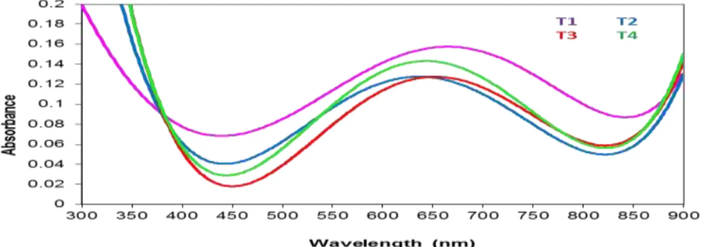
The Optical Reflectance and Refractive Index
Here we will discuss the optical reflectance and refractive indices. As we notice in Figures (5and 6) we see the optical reflective spectrum curves have same optical absorption as a functions of the wavelengths with different temperatures because of the
same reasons obtained by (K.K. Saini ET al.2007). The optical reflectivity values were smaller than optical transmittance because of high transparency.
T=1-(A+R)………. (1).
Where R is optical reflectivity, A is optical absorbance and T is optical transmittance.
Fig. 6: Reflectance values with various temperatures at λ=700 nm
The optical refractive index rises with increasing of wavelength at UV regions and some region of the visible wavelength till to ~ 630 nm and then decreases at other parts ,
these results are degree with (Gao et al., 2004), show Figures (7) and (8) for more details. The refractive index has been calculated by using below equation
2
...
...
...
1
1
)
1
(
4
2 2
R
R
R
K
R
n
N is optical refractive index, R is optical reflectance and K is optical extinction coefficient.
Fig.7: Refractive index with wavelength at different annealig temperatures
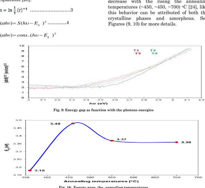
The Optical Energy Gaps
By absorption coefficients energy gaps have been calculated by using the following equations [20].
………..3
L g
E h S
hv) ( )
( …………4
2 ) ..(
)
(hv cons hEg
When r is thickness ,T is optical transmittance and hv is photon energy.
By (αhv) 1/2 we were noting the energy gaps
decrease with the rising the annealing temperatures (~450, ~450, ~700) oC [24], like
this behavior can be attributed of both the crystalline phases and amorphous. See Figures (9, 10) for more details.
Fig. 9: Energy gap as function with the photons energies
Fig. 10: Energy gaps the annealing temperatures
Conclusions
By concentrating observation we saw that region between the wavelengths ~(600-800) nm that optical absorbance rise with increasing the temperature (~460, ~550 and ~700) oC, and say this because growing
crystalline of TiO2 three phases and grain
size growing as well as.
The transmittance values at visible light were normal, especially between ~(600-800) nm was regular and so recognizable, so the transmittance decrease with rising of temperatures (~460,~550 and ~700) oC.
According to the above results conclusions, like those thin films use as a filter of solar cell because of high optical transmittance visible regions and because of r low optical transmittance at uv wavelengths.
The optical reflectivity ware smaller than optical transmittance because of high optical transparency.
The relationship between of the optical refractive index and annealing temperatures was an abnormal and different behavior in the refractive indices and their relationship with annealing temperature. However, in the region after ~630 nm, the results showed that the refractive index rising with an increase in temperature.
References
1. G Korotchenkov (2013) "Thin metal films". Handbook of Gas Sensor Materials. Integrated Analytical Systems. Springer, 153-166. ISBN 978-1-4614-7164-6.
2. Frank FC, Van der Merwe JH (1949) "One-Dimensional Dislocations. II. Misfit ting Monolayer’s and Oriented Overgrowth". Proceedings of the Royal Society of London. Series A, Mathematical and Physical Sciences, 198 (1053): 216-225.
3. M Ohring (2001) Materials Science of Thin Films (2nd Ed.). Boston: Academic Press. ISBN 9780125249751.
4. Pearce J, Lau A (2002) "Net Energy Analysis for Sustainable Energy Production from Silicon Based Solar Cells". ISBN 978-0-7918-1689-9. 5. K Seshan, ed. (2012) Handbook of Thin Film
Deposition (3rd ed.). Amsterdam: Elsevier. ISBN 978-1-4377-7873-1.
6. Mahan, John E (2000) Physical Vapor Deposition of Thin Films. New York: John Wiley & Sons, ISBN 0-471-33001-9.
7. Madou MJ (2002) "Fundamentals of Micro fabrication: The science of Miniaturization" 2nd Ed., CRC Press, 135-6.
8. MW Thompson (1962) "Energy spectrum of ejected atoms during the high- energy sputtering of gold". Phil. Mag., 18 (152): 377. 9. Ohtomo A, Hwang HY (2007) "Growth mode
control of the free carrier density in SrTiO [sub 3-δ] films". Journal of Applied Physics, 102 (8): 083704.
10. DA Karpov (1997) "Cathodic arc sources and macro particle are filtering", Surface and Coatings technology, 96: 22-23.
11. Wall, Staffan (2010) "The history of electro kinetic phenomena." Current Opinion in Colloid & Interface Science 15.3 (2010): 119-124.
12. I.R. Peterson, "Langmuir Blodgett Films ", J. Phys. D 23, 4, (1990) 379–95.
13. Wilson SK, Hunt R, Duffy BR (2000) "The rates of spreading in spin coating". J. Fluid Mech. 413: 65-88.
14. Scriven LE (1988) "Physics and applications of dip coating and spin coating". Better ceramics through chemistry III, 717-729.
15. Falub CV, Von Kanel, H Isa, F Bergamaschini, R Marzegalli, A Chrastina, D Isella, G Muller, E Niedermann, P Miglio L (15 March 2012) "Scaling Hetero-Epitaxy from Layers to Three-Dimensional Crystals". Science, 335 (6074): 1330-1334.
16. El amrani, A Menous, I Mahiou, L Tadjine, R Touati, A Lefgoum A (2008-10-01). "Silicon nitride film for solar cells". Renewable Energy, 33 (10): 2289-2293.
17. Butt Hans-Jurgen, Graf Karlheinz, Kappl Michael (2013). Physics and Chemistry of Interfaces (Third, Revised Ed.). ISBN 978-3-527-41216-7.
18. Klein LC, Garvey GJ (1980) "Kinetics of the Sol-Gel Transition" Journal of Non-Crystalline Solids, 38: 45.
19. Brinker CJ, GW Scherer (1990) Sol-Gel Science: The Physics and Chemistry of Sol-Gel Processing. Academic Press. ISBN 978-0-12-134970-7.
20. Hench LL, JK West (1990) "The Sol-Gel Process". Chemical Reviews, 90: 33-72.
21. Carp O, Huisman CL, Reller A (2004) Photo induced reactivity of titanium dioxide. Prog. Solid-State Chem., 32: 33-117.
22. Abou-Helal MO, Seeber WT (2002) Appl. Surf. Sci., 195: 53-62.
23. SH Oh, DJ Kim, SH Hahn, EJ Kim (2003) Mater. Lett., 57(26-27). 4151.
24. J Tauc, R Grigorovich, A Vancu (1966) Physics. Stat., 15: 627.