EGIGATEK Bluetooth 4.0 LE
Single Mode module datasheet
Doc. Version : 20141012
Product ID
eGM-A20A/B/C
Product Name Bluetooth 4.0 LE single mode module Firmware Version
Hardware Version Rev.1.0.2
1. DESCRIPTION
Bluetooth v4.0 Low Energy specifies two types(single mode and dual mode) of implementation.
Single mode chips implement the low energy specification and consume a fraction of the power of classic Bluetooth to allow the short-range wireless standard to extend to coin cell battery applications. Single mode BLE is not backwards compatible with previous Bluetooth standards.
Dual mode chips combine low energy with the power of classic Bluetooth and to become a defacto feature in new Bluetooth enabled cellular phones and computers. Dual mode BLE is backwards compatible but targeted to gateway products.
eGM-A20 is product from CSR's single mode BLE solution. CSR µEnergy enables ultra low-power connectivity and basic data transfer for applications previously limited by the power consumption, size constraints andcomplexity of other wireless standards. The CSRµEnergy platform provides everything required tocreate a Bluetooth low energy product with RF, baseband, MCU, qualified Bluetooth v4.0 stack and customer application running on a single IC.
2. FEATURES
■ Bluetooth Low Energy available with CSR1010 QFN ■ Bluetooth v4.0 specification
■ Single mode Bluetooth low energy
■ 7.5dBm Bluetooth low energy maximum TX output power ■ -92.5dBm Bluetooth low energy RX sensitivity
ATT, GATT, SMP, L2CAP, GAP
■ RSSI monitoring for proximity applications ■ <600nA ultra low consumption in dormant mode ■ Integrated 32kHz and 16MHz crystal or system clock ■ Switch-mode power supply
■ Programmable general purpose PIO controller ■ 10-bit ADC ■ 11 digital PIOs ■ 3 analogue AIOs ■ UART ■ 512KB EEPROM ■ 3 PWM modules ■ Wake-up interrupt
■ 64KB RAM and 64KB ROM ■ Watchdog timer
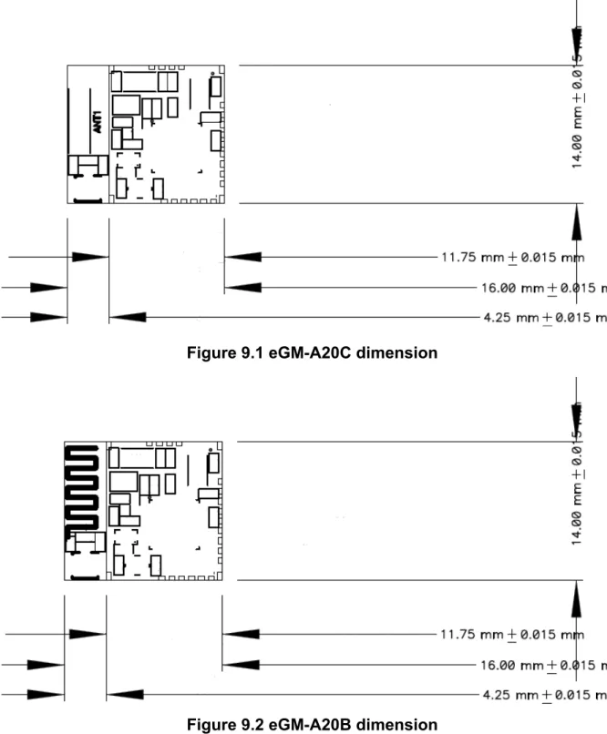
■ Dimensions:
eGM-A20A : 11.75 mm x 14.0 mm x 2.5 mm
eGM-A20B with printed antenna : 16.0 mm x 14.0 mm x 2.5 mm eGM-A20C with chip antenna : 16.0 mm x 14.0 mm x 2.5 mm ■ Storage temperature range: -40ºC ~ +85ºC
■ Operating temperature range: -30ºC ~ +85ºC ■Manufactured in conformance with RoHS
3. APPLICATIONS
Building an ecosystem using Bluetooth low energy
Bluetooth low energy enables the transfer of simple data sets between compact devices opening up a completely new class of Bluetooth applications such as watches, TV remote controls, medical sensors and fitness trainers.
Bluetooth low energy takes less time to make a connection than conventional Bluetooth wireless technology and can consume approximately 1/20th of the power of Bluetooth Basic Rate. Supports profiles for sensors, watches, HIDs and time synchronization.
Typical Bluetooth low energy applications: ■ Sports and fitness
■ Commercial ■ Watches
■ Human interface devices
3.1
Device Details
3.1.1 Bluetooth Radio■ On-chip balun (50Ω impedance in TX and RX modes) ■ No external trimming is required in production
■ Bluetooth v4.0 specification compliant 3.1.2 Bluetooth Transmitter
■ 7.5dBm RF transmit power with level control from integrated 6-bit DAC over a dynamic range >30dB
■ No external power amplifier or TX/RX switch required 3.1.3 Bluetooth Receiver
■ -92.5dBm sensitivity ■ Integrated channel filters
■ Digital demodulator for improved sensitivity and cochannel rejection ■ Fast AGC for enhanced dynamic range
3.1.4 Synthesiser
■ Fully integrated synthesiser requires no external VCO varactor diode, resonator or loop filter
3.1.5 Baseband and Software
■ Hardware MAC for all packet types enables packet handling without the need to involve the MCU
3.1.6 Physical Interfaces ■ SPI master interface
■ SPI programming and debug interface ■ I²C
■ Digital PIOs ■ Analogue AIOs
3.1.7 Auxiliary Features ■ Battery monitor
■ Power management features include software shutdown and hardware wake-up ■ Run in low power modes from an external 32.768kHz clock signal
■ Integrated switch-mode power supply ■ Linear regulator (internal use only)
■ Power-on-reset cell detects low supply voltage 3.1.8 Bluetooth Stack
■ Support for Bluetooth v4.0 specification features: ■ Master and slave operation
■ Including encryption
■ Software stack in firmware includes: ■ GAP
■ L2CAP
■ Security manager ■ Attribute protocol ■ Attribute profile
4. ELECTRICAL CHARACTERISTICS
4.1
Absolute Maximum Ratings
Rating Min Max Unit
Storage temperature -40 +85 ℃
4.2
Recommended Operating Conditions
Operating Condition Min Typ Max Unit
Operating temperature range -30 - 85 ℃
4.3
Input/Output Terminal Characteristics
4.3.1 Digital TerminalsInput Voltage Levels Min Typ Max Unit
VIL input logic level low -0.4 - 0.4 V
VIH input logic level high 0.7 x VDD - VDD+0.4 V
Tr/Tf - - 25 ns
Output Voltage Levels Min Typ Max Unit
VOL output logic level low, lOL = 4.0mA - - 0.4 V
VOH output logic level high, lOH = -4.0mA
0.75 x VDD
- - V
Tr/Tf 1.2 - 5 ns
Input and Tristate Currents Min Typ Max Unit
With strong pull-up -150 -40 -10 µA
I²C with strong pull-up -250 - - µA
With strong pull-down 10 40 150 µA
With weak pull-up -5.0 -1.0 -0.33 µA
With weak pull-down 0.33 1.0 5.0 µA
CI input capacitance 1.0 - 5.0 pF
4.3.2 AIO
Input Voltage Levels Min Typ Max Unit
5.
CURRENT CONSUMPTION
Mode Description Total Typical Current at
3V Dormant All functions are shutdown. To wake up toggle the
WAKE pin.
<600nA Hibernate VDD_PADS = ON, REFCLK = OFF, SLEEPCLK =
ON, VDD_BAT = ON
<1.5µA Deep sleep VDD_PADS = ON, REFCLK = OFF, SLEEPCLK =
ON, VDD_BAT = ON, RAM = ON, digital circuits = ON, SMPS = ON (low-power mode), 1ms wake-up time
<5µA
Idle VDD_PADS = ON, REFCLK = ON, SLEEPCLK = ON, VDD_BAT = ON, RAM = ON, digital circuits = ON, MCU = IDLE, <1µs wake-up time
-1mA
6.
SERIAL INTERFACES
6.1 Application Interface
6.1.1 UART Interface
eGM-A20 provides a simple mechanism for communicating with other serial devices using the RS232 protocol. 2 signals implement the UART function, UART_TX and UART_RX. When eGM-A20 is connected to another digital device, UART_RX and UART_TX transfer data between the 2 devices.
UART configuration parameters, e.g. baud rate and data format, are set using eGM-A20 firmware. When selected in firmware PIO[0] is assigned to a UART_TX output and PIO[1] is assigned to a UART_RX input. The UART CTS and RTS signals can be assigned to any PIO pin by the on-chip firmware.
Note: To communicate with the UART at its maximum data rate using a standard PC, the PC requires an accelerated serial port adapter card.
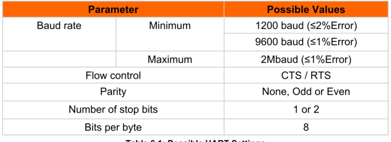
Parameter Possible Values
Baud rate Minimum 1200 baud (≤2%Error)
9600 baud (≤1%Error)
Maximum 2Mbaud (≤1%Error)
Flow control CTS / RTS
Parity None, Odd or Even
Number of stop bits 1 or 2
Bits per byte 8
Table 6.1: Possible UART Settings
6.1.1.1 UART Configuration While in Deep Sleep
The maximum baud rate is 9600 baud during deep sleep.
6.2 SPI Master Interface
The SPI master memory interface in the module is overlaid to uses a further 3 PIOs for the extra pins.
SPI Interface Pin
Flash_VDD PIO[2]
SF_DIN PIO[3]
SF_CS# PIO[4]
SF_CLK I2C_SCL
SF_DOUT I2C_SDA
7. BLOCK DIAGRAM
8. PIN DESCRIPTION
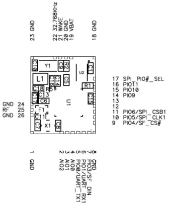
8.1 Pin Numbering
Figure 8.3 eGM-A20A Pin Numbering
8.2 Pin Definition
PIN Name No Description
GND 1 Ground
AIO2 2 Analogue programmable I/O line.
AIO1 3 Analogue programmable I/O line.
AIO0 4 Analogue programmable I/O line.
PIO0 UART_TX1 5 Programmable I/O line or UART TX.
PIO1 UART_RX1 6 Programmable I/O line or UART RX.
PIO3 SF_DIN 7 Programmable I/O line or SPI serial flash data (SF_DIN) input.
GND 8 Ground
PIO4 SF_CS# 9 Programmable I/O line or SPI serial flash chip select (SF_CS#).
PIO5 SPI_CLK1 10 Programmable I/O line or debug SPI CLK
selected by SPI_PIO#.
PIO6 SPI_CSB1 11 Programmable I/O line or debug SPI chip select (CS#) selected by SPI_PIO#.
PIO7 SPI_MOSI1 12 Programmable I/O line or debug SPI MOSI selected by SPI_PIO#.
MOSI selected by SPI_PIO#.
PIO8 SPI_MISO1 13 Programmable I/O line or debug SPI MISO selected by SPI_PIO#
MISO selected MISO selected
PIO9 14 Programmable I/O line.
PIO11 16 Programmable I/O line.
SPI_PIO#_SEL 17 Selects SPI debug on PIO(3.3V SPI mode, 0V PIO mode 10~13) .
GND 18 Ground
VBAT 19 Battery input and regulator enable (active
high).
GND 20 Ground
WAKE 21 Input to wake from hibernate.
32.768KHz_IN 22 Crystal
GND 23 Ground
GND 24 Ground(for eGM-A20A only)
RF 25 Bluetooth transmitter/receiver(for eGM-A20A
only)
9. MECHANICAL CHARACTERICS
9.1 Dimensions
Figure 9.1 eGM-A20C dimension
Figure 9.3 eGM-A20A dimension
9.2 Recommended Land Pattern
Figure 9.5 eGM-A20A land pattern
9.3
Typical Solder Reflow Profile
Temperature profile for reflow soldering9.4 Housing Guidelines
The individual case must be checked to decide whether a specific housing is suitable for the use of the internal antenna. A plastic housing must at least fulfill the following requirements:
² Non-conductive material, non-RF-blocking plastics ² No metallic coating
9.5 Antenna Issues
eGM-A20 is shipped with 3 different antenna designs: eGM-A20C comprises a ceramic antenna which as a component is soldered to the circuit board. This is functional for a eGM-A20B or C integrated into a plastic housing. No additional antenna is required.
For an external antenna to be set in, e.g. because the eGM-A20 is integrated into a metal housing, the ceramic antenna is replaced.
eGM-A20A routes the antenna signal to pin 25. The gain of the external antenna shall not exceed +2dBi.
When using an external Antenna the antenna is fixed and cannot be removed or replaced by the end user. The performance of the internal antenna respectively the external antenna has in any case to be checked within the final integration environment. Adjacent PCBs, components, cables, housings etc. could otherwise influence the radiation pattern or be influenced by the radio wave energy.
It must be ensured that the antenna is not co-located or operating in conjunction with any other antennas, transmitters, cables or connectors. When the internal ceramic antenna is used, certain restrictions are to be considered.
10. APPROVALS/CERTIFICATIONS
The eGM-A20A or B or C has been tested to comply to the appropriate EU, FCC and IC directives. CE testing is intended for end products only. Therefore CE testing is not mandatory for a Bluetooth Module sold to OEM’s. However EGIGA TECHNOLOGIES CO LTD provides CE tested modules for customers in order to ease CE compliance assessment of end products and to minimize test effort.
10.1 Declaration of Conformity CE
The eGM-A20A or B or C fully complies with the essential requirements of the following EU directives:
R&TTE 1999/5/EC (Variant /C for external antenna with less than +2dBi gain) RoHS 2011/65/EC
10.2 FCC Compliance
The eGM-A20B or C has been tested to fulfill the FCC requirements. Test reports are available on request. Grants of the Full Modular Approval will be shown below. eGM-A20A only:
For selling products implementing the eGM-A20A in the USA you’ll have to apply for a Class II Permissive Change from the FCC authorities. Depending on antenna gain and other factors the FCC TCB will issue a reduced test plan for re-testing. EGIGATEK can assist customers with conducting this procedure on request. Especially the test plan reduction and cost optimization may be items worth to look at.
10.2.1 FCC Grant 10.2.2 FCC Statement
This device complies with 47 CFR Part 2 and Part 15 of the FCC Rules and with. Operation is subject to the following two conditions:
(1) this device may not cause harmful interference, and
(2) this device must accept any interference received, including interference that may cause undesired operation.
10.2.4 FCC Warning
You are cautioned that changes or modifications not expressly approved by the part responsible for compliance could void the user’s authority to operate the equipment. This equipment has been tested and found to comply with the limits for a Class B digital device, pursuant to Part 15 of the FCC Rules. These limits are designed to provide reasonable protection against harmful interference in a residential installation. This equipment generates, uses and can radiate radio frequency energy and, if not installed and used in accordance with the instructions, may cause harmful interference to radio communications. However, there is no guarantee that interference will not occur in a particular installation. If this equipment does cause harmful interference to radio or television reception, which can be determined by turning the equipment off and on, the user is encouraged to try to correct the interference by one or more of the following measures:
l Reorient or relocate the receiving antenna.
l Increase the separation between the equipment and receiver.
l Connect the equipment into an outlet on a circuit different from that to which the receiver is connected.
l Consult the dealer or an experienced radio/TV technician for help. 10.2.5 FCC RF Radiation Exposure Statement
The eGM-A20B or C complies with the FCC/ radiation exposure limits set forth for an uncontrolled environment. End users must follow the specific operating instructions for satisfying RF exposure compliance. This transmitter must not be co-located or operating in conjunction with any other antenna or transmitter.
The output power is < 10mW EIRP and therefore according to “FCC KDB 447498 D01 General RF Exposure Guidance v05” Appendix A, table “SAR Exclusion Threshold”, excluded from SAR testing for test separation distances ≥5mm and if it is not used in co-locations with other antennas. If the product implementing the eGM-A20B or C has other antennas in co-location or separation distances < 5mm an FCC TCB should be asked for a Class II Permissive Change.
RF exposure evaluation of devices implementing the eGM-A20A should be done with the collaboration of the FCC TCB working on the Class II Permissive Change Request.
10.2.6 FCC Labeling Requirements for the End Product
Any end product integrating the Model: eGM-A20A or B or C must be labeled with at least the following information:
This device contains transmitter with FCC ID: 2ABQH-eGMA20
10.3 IC Compliance
The eGM-A20A has been tested to fulfill the IC requirements. Test reports RSS-210 of Industry Canada are available on request. Grants of the Full Modular Approval will be shown below.
For selling products implementing the eGM-A20B or C in Canada you’ll have to apply for a Class II Permissive Change from the IC authorities. Depending on antenna gain and other factors the IC TCB will issue a reduced test plan for re-testing. EGIGATEK can assist customers with conducting this procedure on request. Especially the test plan reduction and cost optimization may be items worth to look at.
10.3.1 IC Grant 10.3.2 IC Statement
This device complies with Industry Canada license-exempt RSS standard(s). Operation is subject to the following two conditions:
(1) this device may not cause interference, and
(2) this device must accept any interference, including interference that may cause undesired operation of the device.
Cet appareil numerique de est conforme aux normes canadiennes licence-exempt RSS standard(s).
Son fonctionnement est soumis aux deux conditions suivantes : (1) cet appareil ne doit pas causer d'interference et
(2) cet appareil doit accepter toute interference, notamment les interferences qui peuvent affecter son fonctionnement.
10.3.3 IC Caution
Warning: Changes or modifications made to this equipment not expressly approved by EGIGA TECHNOLOGIES CO LTD may void the IC authorization to operate this equipment.
Request.
10.3.5 IC Labeling Requirements for the End Product
Any end product integrating the Model: eGM-A20A or B or C must be labeled with at least the following information:
This device contains transmitter with IC-ID: 11696A-eGMA20
10.3.6 IC Label Information
The eGM-A20 shows IC-ID on the product label. IC allows to state the IC-ID in the product manual. This product has been granted to do so.
Model: eGM-A20A or B or C The IC-ID is: 11696A-eGMA20
10.4 TELEC Compliance
10.5 Bluetooth Qualification
The eGM-A20 is a qualified design according to the Bluetooth Qualification Program Reference Document (PRD) V2.1 The Qualified Design ID (QDID) is:
B022156
According to the Bluetooth SIG rules (Qualification Program Reference Document – PRD V2.1) you are required to perform the mandatory End Product Listing (EPL) for your product.
10.6 RoHS/SVHC Declaration
The actual version of RoHS Supplier Declaration according to the EU Directive 2011/65/EC.
11. PACKAGE
Tray Type
a. Carrier not be exceed 1mm in 100mm.
b. Packing dimensions meet : 390mm * 270mm * 15mm c. Material : white anti-static polystyrene
d. Component load per tray : 100pcs