Tunable Versatile High Input Impedance Voltage-Mode
Universal Biquadratic Filter Based on DDCCs
Jiun-Wei HORNG, To-Yao CHIU, Zih-Yang JHAO
Dept. of Electronic Engineering, Chung Yuan Christian University, Chung-Li, 32023, Taiwan [email protected]
Abstract. A high input impedance voltage-mode universal biquadratic filter with three input terminals and seven output terminals is presented. The proposed circuit uses three differential difference current conveyors (DDCCs), four resistors and two grounded capacitors. The proposed circuit can realize all the standard filter functions, namely, lowpass, bandpass, highpass, notch and allpass, simulta-neously. The proposed circuit offers the features of high input impedance, using only grounded capacitors, and orthogonal controllability of resonance angular frequency and quality factor.
Keywords
Current conveyor, biquadratic filter, active circuit, voltage-mode.
1.
Introduction
The differential difference current conveyors (DDCC) [1] or differential voltage current conveyors (DVCC) [2], [3] have received considerable attention on realizing multi-function filters and oscillators. This is due to the fact that the addition and subtraction operations for voltage signals can be performed easily.
High input impedance voltage-mode active filters are of great interest because several cells of this kind can be directly connected in cascade to implement higher order filters [4]-[6]. Besides the use of only grounded capacitors and resistors are beneficial from the point of view of inte-grated circuit fabrications [7]-[9].
Several high input impedance voltage-mode universal biquads each with multi-input terminals were presented in [5], [10]-[14]. Five kinds of standard filter functions can be derived by the selections of different input voltage termi-nals in these circuits. However, only one standard filter function can be obtained in each realization of [5], [10]-[12]. Moreover, four kinds of standard filter functions at most can be obtained, simultaneously, in each circuit reali-zation of [13], [14]. Moreover, the resonance angular fre-quencies and quality factors of these circuits cannot be orthogonally controllable. Three multi-inputs and one
out-put universal biquads were presented in [15]-[17]. Al-though the resonance angular frequencies and quality fac-tors of these circuits can be orthogonally controllable, they require passive components matching conditions in the realizations of some filter functions. Two high input im-pedance three-inputs and one output universal biquads were presented in [18]. However, the resonance angular frequency and quality factor of the first proposed circuit cannot be orthogonally controllable and both circuits re-quire passive components matching conditions in the reali-zation of allpass filter functions.
The circuits that consist of more filter functions mean more applications they can be used. Therefore, many high input impedance circuits that can realize all of the standard filter functions; namely highpass, bandpass, lowpass, notch and allpass from the same circuit configuration simultane-ously were presented in the literatures [15], [19]-[25]. However, the resonance angular frequencies and quality factors of the circuits in [15], [19], [20] cannot be orthogonally controllable. The circuits in [21]-[25] have the feature of orthogonally controllable of resonance angular frequencies and quality factors but they use floating resistors.
In this paper, a new high input impedance voltage-mode universal biquadratic filter with three input terminals and seven output terminals using three DDCCs is pre-sented. The proposed circuit uses four resistors and two grounded capacitors. The proposed circuit has the follow-ing features: (i) high input impedance, (ii) usfollow-ing only grounded capacitors, (iii) five kinds of standard filter func-tions can be obtained simultaneously from the same circuit configuration, and (iv) orthogonal controllability of reso-nance angular frequency and quality factor. Moreover, if one of the output terminals at the proposed circuit is not required (deleted), five kinds of filter functions still can be obtained from the circuit by appropriate selecting the input terminals. This circuit configuration needs not passive component matching condition in the realization of all filter types and using only grounded passive components. With respect to the multi-inputs universal biquads in [5], [10]-[14], the resonance angular frequency and quality factor can be orthogonally controllable in the proposed circuit. With respect to the three inputs universal biquads in [15]-[18], the proposed circuit needs no passive
compo-nents matching conditions in the realization of allpass filter functions. Comparisons of some multi-inputs biquads are given in Tab. 1. Tab. 1 shows the features of the proposed circuit in orthogonally controllable of resonance angular frequency and quality factor and using only grounded pas-sive components. Comparisons of some multi-outputs biquads that can realize all of the standard filter functions simultaneously are given in Tab. 2.
2.
Circuit Description
Using standard notation, the port relations of an ideal DDCC can be characterized by
zk z x y y y zk z y y y xv
v
i
v
v
v
i
...
i
i
i
i
v
...
0
...
0
1
0
0
0
...
...
...
...
...
...
...
0
...
0
1
0
0
0
0
...
0
0
0
0
0
0
...
0
0
0
0
0
0
...
0
0
0
0
0
0
...
0
0
1
1
1
1 3 2 1 1 3 2 1 (1)where the plus and minus signs indicate whether the con-veyor is configured as a non-inverting or inverting type circuit, termed DDCC+ or DDCC-.
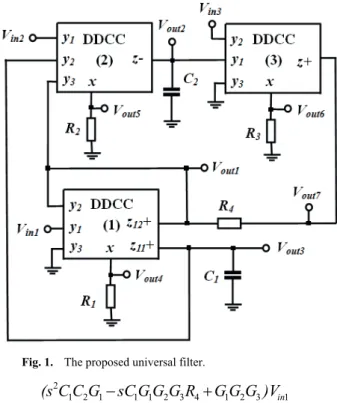
The proposed configuration is shown in Fig. 1. The output voltages can be expressed as:
3 2 1 3 2 1 1 2 1 2 3 3 2 1 2 2 3 2 1 1 3 2 1 1 2 1 2 1 ) ( G G G G G sC G C C s V G C C s V G G sC V G G G G C C s V in in in out (2) 3 2 1 3 2 1 1 2 1 2 3 3 2 1 3 2 1 2 2 1 1 1 2 1 1 2 s CCG sCGG GGG )V G G G G G (sC V G G sC V G G sC V in in in out (3) 3 2 1 3 2 1 1 2 1 2 3 3 1 2 2 3 2 1 1 3 2 1 3 G G G G G sC G C C s V G G sC V G G G V G G G V in in in out (4) 3 2 1 3 2 1 1 2 1 2 3 3 2 1 2 2 3 2 1 1 3 2 1 4 G G G G G sC G C C s V G C C s V G G sC V G G sC V in in in out (5) 3 2 1 3 2 1 1 2 1 2 3 3 1 2 3 2 1 2 2 1 2 1 2 1 1 2 1 2 5 ) ( G G G G G sC G C C s V G G sC G C C s V G C C s V G C C s V in in in out (6) 3 2 1 3 2 1 1 2 1 2 3 1 2 1 2 2 2 1 1 1 2 1 1 6 G G G G G sC G C C s V G C C s V G G sC V G G sC V in in in out (7)
Fig. 1. The proposed universal filter.
3 2 1 3 2 1 1 2 1 2 3 4 3 1 2 1 2 3 2 1 2 2 4 3 2 1 1 3 2 1 1 3 2 1 4 3 2 1 1 1 2 1 2 7 ) ( ) ( G G G G G sC G C C s V R G G C C s G C C s V R G G G sC G G sC )V G G G R G G G sC G C C (s V in in in out (8) From (2)–(8), we can see that six circuit types can be obtained from Fig. 1:
(1) If Vin2 = Vin3 = 0 (grounded); Vin1 = input voltage
signal, a notch filter can be obtained at Vout1, three
band-pass filters can be obtained at Vout2, Vout4 and Vout6, a
low-pass filter can be obtained at Vout3, a highpass filter can be
obtained at Vout5 and and if R4 = R1, an allpass filter can be
obtained at Vout7.
(2) If Vin1= Vin3 = 0 (grounded); Vin2 = input voltage
signal, five bandpass filters can be obtained at Vout1, Vout2, Vout4, Vout6and Vout7, a lowpass filter can be obtained at Vout3, and a highpass filter can be obtained at Vout5.
(3) If Vin1= Vin2 = 0 (grounded); Vin3 = input voltage
signal, four highpass filters can be obtained at Vout1, Vout4, Vout6and Vout7 and a bandpass filter can be obtained at Vout3.
(4) If Vin3 = 0 (grounded), then Vin1 = Vin2 = input
volt-age signal, an allpass filter can be obtained at Vout1, three
bandpass filters can be obtained at Vout2, Vout4 and Vout6,
a lowpass filter can be obtained at Vout3 and a highpass
filter can be obtained at Vout5.
(5) If Vin2 = 0 (grounded), then Vin1 = Vin3 = input
volt-age signal and R3 = R1, two lowpass filters can be obtained
at Vout1 and Vout2 and a bandpass filter can be obtained at Vout5.
(6) If Vin1 = 0 (grounded), then Vin2 = Vin3 = input
volt-age signal and R3 = R1, a lowpass filter can be obtained at Vout2 and a bandpass filter can be obtained at Vout5.
Active device Needs inverting inputs Grounded passive components Floating passive components Matching constraints High input impedance ωo/Q orthogonal controllability Kinds of filter functions simultaneously [5] three CCIIs yes 0 4 no yes no 1 [10] three DDCCs no 4 0 no yes no 1 [11] one DDCC one FDCCII no 4 0 no yes no 1 [12] three DDCCs no 5 0 yes yes no 1 [13] three DDCCs no 4 0 no yes no 4 [14] One DDCC one FDCCII no 4 0 no yes no 4 [15] Fig. 3 three DVCCs
no 5 0 yes yes yes 1
[16] four CFAs
no 3 4 yes yes yes 1
[17] three CFAs
no 4 3 yes yes yes 1
[18], Fig. 1 three DVCCs no 5 1 yes yes no 1 [18], Fig. 2 two DVCCs one DDCC
no 6 0 yes yes yes 1
New circuit
three DDCCs
no 5 0 no yes yes 4
Tab. 1. Comparisons of some multi-inputs biquads (The resistor R4 in the proposed circuit is shorted).
Active device Grounded passive components Floating passive components Matching constraints High input impedance ωo/Q orthogonal controllability [15], Fig. 2 three DVCCs 5 0 yes yes no [19], Fig. 1 two FDCCIIs 4 0 no yes no [20] three DDCCs 3 1 no yes no [21] five CFAs
5 3 yes yes yes
[22] two DVCCs
3 2 yes no yes
[23] three DVCCs
3 2 yes yes yes
[24] three DDCCs
4 1 no yes yes
[25] three DVCCs
4 2 yes yes yes
New circuit
three DDCCs
5 1 yes yes yes
The resonance angular frequency 0 and quality
factor Q are obtained by
2 1 3 2 C C G G o
, (9) 3 2 1 2 1 G G C C G Q . (10)In first circuit type, all standard filter functions can be simultaneously obtained from the same circuit configura-tion. If the output terminal Vout7 is not required, the floating
resistor R4 is not needed and can be shorted. Note that if
the output terminal Vout7 is not needed, five kinds of filter
functions still can be realized by appropriate selecting the input terminals without component matching condition and using only grounded passive components.
The proposed circuit uses grounded capacitors, which are attractive for integrated circuit implementation [7]. Due to the three input signals, Vin1, Vin2 and Vin3, are connected
to the high input impedance input nodes of the three DDCCs (the y port of the DDCC), respectively, the pro-posed circuit enjoys the feature of high input impedance. From (9), (10), the resonance angular frequency can be controlled by R2 or R3. The quality factor can be
independ-ently controlled by R1. Therefore, the resonance angular
frequency and quality factor can be orthogonally controlla-ble.
3.
Sensitivities Analysis
Taking the non-idealities of the DDCC into account, the relationship of the terminal voltages and currents can be rewritten as x y y y k k k k z y y y x i v v v s s s s i i i i v 3 2 1 3 2 1 3 2 1 ) ( 0 0 0 0 0 0 0 0 0 0 0 0 0 0 0 0 ) ( ) ( ) (
(11)where k1(s), k2(s), and k3(s) represent the frequency
transfer functions of the internal voltage followers and k(s) represent the frequency transfer function of the
inter-nal current follower of the k-th DDCC. They can be ap-proximated by first order lowpass functions, which can be considered to have a unity value for frequencies much lower than their corner frequencies [2]. If the circuit is working at frequencies much lower than the corner fre-quencies of k1(s), k2(s), k3(s) and k(s), then
k1(s) = k1 = 1 - k1 and k1 (k1 << 1) denotes the volt-age tracking error from y1 terminal to x terminal of the k-th
DDCC, k2(s) = k2 = 1 - k2 and k2 (k2 << 1) denotes
the voltage tracking error from y2 terminal to x terminal of
the k-th DDCC, k3(s) = k3 = 1 - k3 and k3 (k3 << 1) denotes the voltage tracking error from y3 terminal to x
terminal of the k-th DDCC and k(s) = k = 1 - ki and ki
(ki << 1) denotes the current tracking error of the k-th
DDCC. The denominator of the non-ideal output voltage function for Fig. 1 becomes
3 2 11 31 22 12 3 2 1 3 2 31 23 3 2 1 12 12 1 2 1 2 β β β α α α G G G β β α α G G sC G C C s D(s)
. (12) The resonance angular frequency 0 and qualityfactor Q become , 12 2 1 3 2 11 31 22 3 2
C C β β β α G G o (13) . 3 2 31 3 2 1 12 11 22 2 23 12 1 β β G G C β α C G Q
(14)The active and passive sensitivities of 0 and Q are
shown as 2 1 2 1 3 2 12 3 2 11 31 22, , , , , , o o o o C C G G S S S S ; 1 1 23 12 Q G Q Q S S S ; ; 2 1 3 2 31 12 11 22, , , , Q Q S S 2 1 3 2 1 2 , , Q G G C Q C S S .
All the active and passive sensitivities are no larger than 1.
4.
Influence of Parasitic Elements
A non-ideal DDCC model is shown in Fig. 2 [26]. It is shown that the real DDCC has parasitic resistors and capacitors from the y1, y2, y3 and z terminals to the ground,
and also, a series resistor at the input terminal x. Taking into account the non-ideal DDCCs and assuming the cir-cuits are working at frequencies much lower than the cor-ner frequencies of i(s), and j(s), namely, ij 1.
Moreover, in practical DDCCs, the external resistors can be chosen to be much smaller than the parasitic resistors at the y and z terminals of DDCCs and much greater than the parasitic resistors at the x terminals of DDCCs, i.e. Ry, Rz
>> Rk >> Rx. The external capacitances C1 and C2 can be
chosen to be much greater than the parasitic capacitors at the y and z terminals of DDCCs, i.e. Cy, Cz << C1, C2.
Furthermore, assuming that the resistances R4 = R1 and the
parasitic capacitances at the y terminals and z terminals of the DDCCs are equal, i.e. Cy Cz.
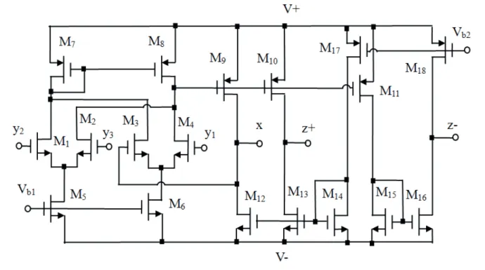
Fig. 3. The CMOS realization of the DDCC.
Fig. 2. The non-ideal DDCC model.
Under these conditions, the denominator of Fig. 1 becomes ' ' ' ' ' ' ' ' ' ' ' ' ' 4 ' ' 2 ) ( 3 2 2 1 3 2 1 1 2 1 2 1 2 1 2 1 3 2 2 1 4 G G G G G G sC G C C s G C C C s C C C s s D z z (15) where 22 11 1 1' C Cz Cy C
,
C2' C2 Cz2 Cy31,
1 1 1' R Rx R ,
R2' R2 Rx2,
R3' R3Rx3.
In (15), undesirable factors are yielded by the non-idealities of the DDCCs. The capacitance Cz becomes
effective at very high frequency. To minimize the effects of the DDCCs’ non-idealities, the operation angular fre-quency should be restricted to the following conditions
min { z C R' 2 1 1 , ' ' ' 1 2 1 3 2 2C R R C z }. (16) Moreover, application of the Routh-Hurwitz test to the denominator of (15) shows that Cz may causeinstabil-ity. According to this test, the transfer functions is stable if } ' ' 2 ' ' ' ' ' 8 ), ' 2 ' ' ( max{ ' 2 1 1 3 2 1 2 1 2 2 1 3 2 2 C G G G C G C C G G G C C z z . (17)
It is not difficult to satisfy this condition, since the external capacitance C2 can be chosen very much greater
than Cz.
5.
Simulation Results
HSPICE simulations were carried out to demonstrate the feasibility of the proposed circuit in Fig. 1. The DDCC was realized by the CMOS implementation of Elwan and Soliman [2] (by ungrounding the gate of MOSFET M2 and
treating this as the third y-input y3) and is redrawn in
Fig. 3. The simulations use TSMC (Taiwan Semiconductor Manufacturing Company, Ltd.) 0.18μm level 49 CMOS technology process parameters. The supply voltages are
V+ = +1.25 V, V- = -1.25 V, Vb1 = -0.45 V and Vb2 = 0.3 V.
The dimensions of the NMOS transistors in the DDCC are set to be W = 4.5 μm and L = 0.9 μm. The dimensions of the PMOS transistors in the DDCC are set to be W = 9 μm and L = 0.9 μm. Fig. 4 (a)-(g) represent the simulated fre-quency responses for the notch (Vout1), inverting bandpass
(Vout2), lowpass (Vout3), bandpass (Vout4), highpass (Vout5),
Fig. 1, respectively, designed with Vin2 = Vin3 = 0
(grounded), Vin1 = input voltage signal, Q = 1 and fo = 1.5915 MHz: C1= C2 = 10 pF and R1 = R2 = R3 = R4=
10 k. Fig. 5 represents the INOISE and ONOISE simula-tion results of the bandpass filter at Vout4. Fig. 6 shows the
the total harmonic distortion (THD) of the Vout2 and Vout4
(a)
(b)
(c)
output voltages (bandpass signals). They are given at 1.5915 MHz operation frequency with Vin1 = input voltage
signal, Vin2 = Vin3 = 0 (grounded) and Q = 1: C1 = C2 =
10 pF and R1 = R2 = R3= R4 = 10 k. Fig. 6 shows that the
THDs of Vout2 and Vout4 are less than 3 percent at 1000 mV
output voltages (peak to peak).
(d)
(e)
(g)
Fig. 4. Simulated frequency responses of Fig. 1 designed with
Vin2 = Vin3 = 0 (grounded), Vin1 = input voltage signal:
(a) notch filter (Vout1), (b) inverting bandpass filter
(Vout2), (c) lowpass filter (Vout3), (d) bandpass filter
(Vout4), (e) highpass filter (Vout5), (f) inverting bandpass
filter (Vout6), (g) allpass filter (Vout7).
Fig. 5. INOISE and ONOISE simulation results of the
proposed bandpass filter at Vout4.
Fig. 6. THD analysis results of the proposed bandpass filters at Vout2 and Vout4.
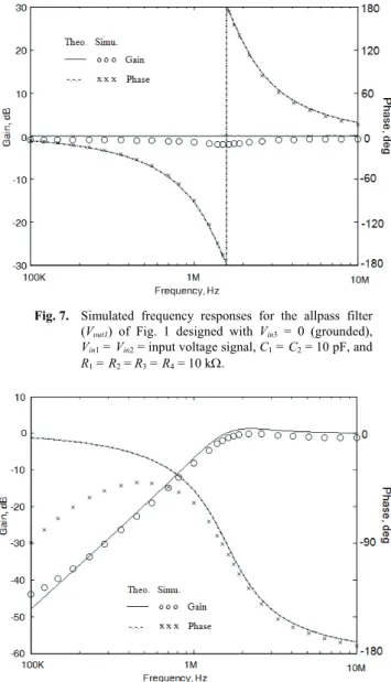
Fig. 7 represents the simulated frequency responses for the allpass (Vout1) filter of Fig. 1, designed with Vin3 = 0
(grounded), Vin1 = Vin2 = input voltage signal, Q = 1 and fo
= 1.5915 MHz: C1 = C2 = 10 pF and R1 = R2 = R3 = R4=
10 k. Fig. 8 represents the simulated gain responses for the inverting highpass (Vout1) filter of Fig. 1, designed with Vin1 = Vin2 = 0 (grounded); Vin3 = input voltage signal, Q =
1 and fo = 1.5915 MHz: C1 = C2 = 10 pF and R1= R2 = R3
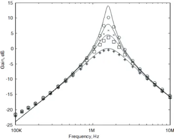
= R4= 10 k. Fig. 9 represents the simulated frequency
responses for the inverting bandpass (Vout2) filter of Fig. 1
as the resistor R1 in Q is varied designed with Vin2 = Vin3 =
0 (grounded) and Vin1 = input voltage signal: C1 = C2 =
10 pF and R2 = R3 = R4= 10 k. The quality factor was
found to vary as 3.157, 1.988, 1.468 and 0.994 for four values of R1as 2 k, 4 k, 6 k and 10 k, respectively.
All the simulation results are coherent and support the theoretical analyses.
Fig. 7. Simulated frequency responses for the allpass filter (Vout1) of Fig. 1 designed with Vin3 = 0 (grounded), Vin1= Vin2 = input voltage signal, C1 = C2 = 10 pF, and R1 = R2 = R3= R4 = 10 k.
Fig. 8. Simulated gain responses for the highpass filter (Vout1)
of Fig. 1 designed with Vin1 = Vin2 = 0 (grounded); Vin3 = input voltage signal, C1 = C2 = 10 pF, and R1 = R2 = R3= R4 = 10 k.
Fig. 9. Simulated frequency responses for the inverting bandpass filter of Fig. 1 designed with C1 = C2 = 10 pF
and R2 = R3 = R4 = 10kΩ.
____ , ideal curve; o o o, R1 = 2 kΩ; x x x, R1 = 4 kΩ;
□ □ □,R1 = 6 kΩ; * * *, R1 = 10 kΩ.
The DDCC has parasitic resistor from the z terminal to the ground (Rz) [26]. When the z terminal load of the
DDCC is a capacitor (C), it introduces a pole produced by
Rz and C at low frequency. This can explain why Fig. 4(b),
4(d), 4(f) and Fig. 8 have non-ideal phase responses at low frequencies. This effect can be minimized by using larger loading capacitors.
6.
Conclusion
In this paper, a new high input impedance voltage-mode universal biquadratic filter with three input terminals and seven output terminals is presented. The proposed circuit uses three DDCCs, four resistors and two grounded capacitors and offers the following advantages: high input impedance, the use of only grounded capacitors, the versa-tility to synthesize lowpass, bandpass, highpass, notch, and allpass responses, simultaneously and orthogonal control-lability of resonance angular frequency and quality factor. Finally, it should be mentioned that if the output ter-minal Vout7 at the proposed circuit is not required, the
float-ing resistor R4 can be deleted. Note that five kinds of filter
functions still can be obtained from this circuit by appro-priate selecting the input terminals. This circuit configura-tion needs not passive component matching condiconfigura-tion in the realizations of all filter functions and using only grounded passive components.
Acknowledgment
The authors would like to thank the reviewers for their suggestions. The National Science Council, Republic of China supported this work under grant number NSC 101-2221-E-033-070.
References
[1] CHIU, W., LIU, S. I., TSAO, H. W., CHEN, J. J. CMOS differential difference current conveyors and their applications.
IEE Proceedings-Circuits Devices and Systems, 1996, vol. 143, p. 91-96.
[2] ELWAN, H. O., SOLIMAN, A. M. Novel CMOS differential voltage current conveyor and its applications. IEE Proceedings-Circuits, Devices and Systems, 1997, vol. 144, p. 195-200. [3] PAL, K. Modified current conveyors and their applications.
Microelectronics Journal, 1989, vol. 20, p. 37-40.
[4] FABRE, A., DAYOUB, F., DURUISSEAU, L., KAMOUN, M. High input impedance insensitive second-order filters implemented from current conveyors. IEEE Transactions on Circuits and Systems-I: Fundamental Theory and Applications, 1994, vol. 41, p. 918-921.
[5] HORNG, J. W. High-input impedance voltage-mode universal biquadratic filter using three plus-type CCIIs. IEEE Transactions on Circuits and Systems-II: Analog and Digital Signal Processing, 2001, vol. 48, p. 996-997.
[6] KOTON, J., HERENCSAR, N., VRBA, K. KHN-equivalent voltage-mode filters using universal voltage conveyors. AEU International Journal of Electronics and Communications, 2011, vol. 65, p. 154-160.
[7] BHUSHAN, M., NEWCOMB, R.W. Grounding of capacitors in integrated circuits. Electronics Letters, 1967, vol. 3, p. 148-149. [8] CHANG, C. M., SOLIMAN, A. M., SWAMY, M. N. S. Analytical
synthesis of low-sensitivity high-order voltage-mode DDCC and FDCCII-grounded R and C all-pass filter structures. IEEE Transactions on Circuits and Systems I: Regular Papers, 2007, vol. 54, p. 1430-1443.
[9] GUPTA, S.., SENANI, R. Realisation of current-mode SRCOs using all grounded passive elements. Frequenz, 2003, vol. 57, p. 26-37.
[10] CHIU, W. Y., HORNG, J. W. High-input and low-output impedance voltage-mode universal biquadratic filter using DDCCs. IEEE Transactions on Circuits and Systems Part II: Express Briefs, 2007, vol. 54, p. 649-652.
[11] CHEN, H. P., YANG, W. S. High-input and low-output impedance voltage-mode universal DDCC and FDCCII filter. IEICE Transactions on Electronics, 2008, vol. 91-C, p. 666 - 669. [12] LEE, C. N. Fully cascadable mixed-mode universal filter biquad
using DDCCs and grounded passive components. Journal of Circuits, Systems, and Computers, 2011, vol. 20, p. 607 - 620. [13] HORNG, J. W. High input impedance voltage-mode universal
biquadratic filter with three inputs using DDCCs. Circuits, Systems, and Signal Processing, 2008, vol. 27, p. 553-562. [14] CHEN, H. P. Versatile multifunction universal voltage-mode
biquadratic filter. AEU International Journal of Electronics and Communications, 2010, vol. 64, p. 983-987.
[15] MINAEI, S., YUCE, E. All-grounded passive elements voltage-mode DVCC-based universal filters. Circuits, Systems, and Signal Processing, 2010, vol. 29, p. 295-309.
[16] NIKOLOUDIS, S., PSYCHALINOS, C. Multiple input single output universal biquad filter with current feedback operational amplifiers. Circuits, Systems, and Signal Processing, 2010, vol. 29, p. 1167-1180.
[17] TOPALOGLU, S., SAGBAS, M., ANDAY, F. Three-input single-output second-order filters using current-feedback amplifiers. AEU International Journal of Electronics and Communications, 2012, vol. 66, p. 683-686.
[18] HORNG, J. W., HSU, C. H., TSENG, C. Y. High input impedance voltage-mode universal biquadratic filters with three inputs using three CCs and grounding capacitors. Radioengineering, 2012, vol. 21, p. 290-296.
[19] CHEN, H. P. Voltage-mode FDCCII-based universal filters. AEU International Journal of Electronics and Communications, 2008, vol. 62, p. 320-323.
[20] HORNG, J. W., CHIU, W. Y. High input impedance DDCC-based voltage-mode universal biquadratic filter with three inputs and five outputs. Indian Journal of Engineering & Materials Sciences, 2011, vol. 18, p. 183-190.
[21] ABUELMA’ATTI, M. T., AL-ZAHER, H. A. New universal filter with one input and five outputs using current-feedback amplifiers.
Analog Integrated Circuits and Signal Processing, 1998, vol. 16, p. 239-244.
[22] HORNG, J. W. Lossless inductance simulation and voltage-mode universal biquadratic filter with one input and five outputs using DVCCs. Analog Integrated Circuits and Signal Processing, 2010, vol. 62, p. 407-413.
[23] MAHESHWARI, S., MOHAN, J., CHAUHAN, D. S. High input impedance voltage-mode universal filter and quadrature oscillator.
Journal of Circuits, Systems, and Computers, 2010, vol. 19, p. 1597- 1607.
[24] CHIU, W. Y., HORNG, J. W. High input impedance voltage-mode universal biquadratic filter with three inputs and six outputs using three DDCCs. Circuits, Systems and Signal Processing, 2012, vol. 31, p. 19-30.
[25] HORNG, J. W., HOU, C. L, CHANG, C. M., CHOU, H. P., LIN, C. T. High input impedance voltage-mode universal biquadratic filter with one input and five outputs using current conveyors.
Circuits, Systems and Signal Processing, 2006, vol. 25, p. 767-777. [26] MAHESHWARI, S. Quadrature oscillator using grounded
compo-nents with current and voltage outputs. IET Circuits, Devices and Systems, 2009, vol. 3, p. 153-160.
About Authors ...
Jiun-Wei HORNG was born in Tainan, Taiwan, Republic of China, in 1971. He received the B.S. degree in Elec-tronic Engineering from Chung Yuan Christian University, Chung-Li, Taiwan, in 1993, and the Ph.D. degree from National Taiwan University, Taipei, Taiwan, in 1997. From 1997 to 1999, he served as a Second-Lieutenant in China Army Force. From 1999 to 2000, he joined CHROMA ATE INC. where he worked in the area of video pattern generator technologies. Since 2000, he was with the Department of Electronic Engineering, Chung Yuan Christian University, Chung-Li, Taiwan. He is now a Professor. Dr. Horng joins the Editorial Board of Active and Passive Electronic Components from 2010. He joins the Editorial Board of Radioengineering from 2011. He joins the Editorial Board of Journal of Engineering from 2012. His teaching and research interests are in the areas of circuits and systems, analog electronics, active filter design and current-mode signal processing.
To-Yao CHIU is now working toward the M.S. degree in Electronic Engineering at Chung Yuan Christian Univer-sity, Chung-Li, Taiwan. His research interests are in the area of analog filter design, electronic circuit design and simulation.
Zih-Yang JHAO is now working toward the M.S. degree in Electronic Engineering at Chung Yuan Christian Univer-sity, Chung-Li, Taiwan. His research interests are in the area of analog filter design, electronic circuit design and simulation.