High Input Impedance Voltage-Mode Biquad Filter
Using VD-DIBAs
Winai JAIKLA
1, Dalibor BIOLEK
2,3, Surapong SIRIPONGDEE
1, Josef BAJER
21 Dept. of Engineering Education, Faculty of Industrial Education, King Mongkut’s Institute of Technology Ladkrabang,
Bangkok, 10520, Thailand
2 Dept. of Electrical Engineering, Faculty of Military Technology, University of Defense Brno, Kounicova 65,
662 10 Brno, Czech Republic
3 Dept. of Microelectronics, Faculty of Electrical Engineering and Communications, Brno University of Technology,
Technická 10, 616 00 Brno, Czech Republic
[email protected], [email protected], [email protected], [email protected]
Abstract. This paper deals with a single-input multiple-output biquadratic filter providing three functions (low-pass, high-pass and band-pass) based on voltage differ-encing differential input buffered amplifier (VD-DIBA). The quality factor and pole frequency can be electronically tuned via the bias current. The proposed circuit uses two VD-DIBAs and two grounded capacitors without any ex-ternal resistors, which is suitable to further develop into an integrated circuit. Moreover, the circuit possesses high input impedance, providing easy voltage-mode cascading. It is shown that the filter structure can be easily extended to multi-input filter without any additional components, providing also all-pass and band-reject properties. The PSPICE simulation results are included, verifying the key characteristics of the proposed filter. The given results agree well with the theoretical presumptions.
Keywords
Analog filter, VD-DIBA, voltage-mode, single input-multiple output.
1.
Introduction
Analog active filter is one of the standard research topics in the circuit design. It is commonly utilized block for continuous-time analog signal processing. It is gener-ally used in many fields, such as communications, meas-urement, instrumentation, and control systems [1]. Espe-cially, the filters providing several functions within a single topology, namely the universal or multifunction filter, have been receiving considerable attention. One of the most popular analog filters is a single-input, multiple-output (SIMO) topology in which various transfer functions can be realized simultaneously. The SIMO topology can be found in many applications, for example in touch-tone telephone tone decoder, in phase-locked loop FM stereo demodulator, or in crossover network as a part of the three-way high-fidelity loudspeaker [2].
The design of analog circuits using active building blocks, taking into account several various criteria such as minimum number of active elements or others, has been receiving considerable attention. Biolek et al. [3] proposed several circuit ideas of building blocks for voltage-, cur-rent- and mixed mode applications. One of them is the voltage differencing differential input buffered amplifier (VD-DIBA). This device allows applications with inter-esting features, especially those providing the electronic controllability. It is obvious from the literature survey that a few circuits using VD-DIBA have been hitherto pub-lished, for instance the voltage-mode first-order allpass filter [4], inductance simulator [5], and multiple-input sin-gle-output (MISO) voltage-mode biquad filter [6].
This contribution presents a SIMO voltage-mode fil-ter with high input impedance, employing VD-DIBAs. It is suitable for fabricating as a monolithic chip or also for off-the-shelf implementation, consisting of 2 active elements and 2 grounded capacitors. The proposed filter can provide three standard functions (low-pass, high-pass and band-pass). The quality factor and pole frequency can be elec-tronically adjusted.
The paper is organized as follows: In Section 2, which follows this Introduction, the definition and features of the VD-DIBA are given, and the proposed filter is also pre-sented. The non-ideal analysis is included in Section 3. The experimental results, namely SPICE simulations and meas-urements on a filter specimen, are illustrated in Section 4. Section 5 describes the filter extension to multi-input to-pology and transconductance type. The comparison with previous works is described in Section 6. Some concluding remarks are given in Section 7.
2.
Theory and Principle
2.1
VD-DIBA Overview
The principle of VD-DIBA was introduced in [3]. The internal construction of VD-DIBA using commercially
available ICs has been proposed in [4]. Its symbol and equivalent circuit are shown in Fig. 1(a) and (b), where V+ and V- are the voltage input terminals. The voltage is con-verted to the z-terminal current via a transconductance gm, which can be tuned by the bias current. The difference of z- and v- terminal voltages is copied to the w terminal with the differential-input unity gain buffer. An ideal VD-DIBA has low-impedance w terminal and high-impedance v+, v-, z, and v terminals. The characteristics of VD-DIBA can be described as follows: w v z m m w v z v v I V V V V g g V I I I I 0 1 1 0 0 0 0 0 0 0 0 0 0 0 0 0 0 0 0 0 0 0 0 . (1)
v
v
z
v
w
V
wV
wI
vI
vV
zI
zV
vI
vI
V
(a)V
wV
vV
zV
V
( ) m g VV z v VV (b)Fig. 1. VD-DIBA: (a) Symbol. (b) Equivalent circuit.
2.2
High Input Impedance Voltage-Mode
Filter Using VD-DIBAs
The proposed second-order filter is illustrated in Fig. 2. It consists of two VD-DIBAs and two grounded capacitors. It is obvious that the proposed filter provides simultaneously three frequency responses (HP, LP and BP) with high input impedance property. Considering the ideal VD-DIBA, a routine analysis of the proposed filter pro-vides the following voltage transfer functions:
2 2 2 1 2 1 1 2 HP m m m in V s g g g V s s C C C , (2) 1 2 1 2 2 2 1 2 1 1 2 m m LP m m m in g g V C C g g g V s s C C C , (3) and 2 1 2 2 1 2 1 1 2 m BP m m m in g s V C g g g V s s C C C . (4)
The filter pole frequency (ω0) and quality factor (Q) can be
expressed as 1 2 0 1 2 m m g g C C , (5) and 1 1 2 2 m m C g Q C g . (6)
It follows from (5) and (6) that the quality factor and pole frequency can be tuned electronically via transconduct-ances. v v z v w v vz v w 2 VD DIBA 1 VD DIBA 1 C 2 C Vin HP V BP V LP V
Fig. 2. Proposed voltage-mode filter.
The relative sensitivities of the proposed circuit can be found as plus or minus 0.5:
0 0 0 0 1 2 1 2 1 1 ; 2 2 m m g g C C S S S S , (7) and 2 1 ; 2 1 2 2 1 1 Q g Q C Q g Q C S m S S m S . (8)
As a drawback, the LP and BP outputs are not of low im-pedance characters, thus they should be additionally buff-ered when applicable, or the filter topology should be modified as described in Section 5.
3.
Non-ideal Case
In practice, the influences of voltage tracking errors from the unity-value gain of internal differential voltage buffer, and also the parasitic terminal impedances of VD-DIBA [4] will affect the filter performance. In this Section, these parameters will be taken into account. For non-ideal voltage buffer, its model is as follows:
w z v
Here β+and β- are the voltage error gains from z and v terminals to w terminal. The influences of parasitic imped-ances of the v+, v- and v terminals of VD-DIBA No. 2 and of v+ and v terminals of VD-DIBA No. 1 are negligible because of their connection to low-impedance outputs w, to the input voltage source, or to ground. The most important parasitic impedances are resistive and capacitive parts affecting the z terminals of VD-DIBAs, acting in parallel to C1 and C2. Let us denote them Rz1, Cz1, and Rz2, Cz2,
re-spectively. Taking them into account together with (9), the transfer functions will be modified to the more general forms: D C R s C R s V V z z in HP 1 1 2 2 2 1 1 1 , (10) D C C g g V V m m in LP 1 2 2 1 2 1 , (11) and D C R s C g V V z m in BP 1 2 2 2 2 1 1 (12) where C1C1Cz1, C2 C2Cz2, and 2 * 0 * * 0 2 Q s s D , (13) 2 1 2 1 2 1 2 2 1 2 1 2 1 2 * 0 1 z z m m z m m m R R g g R g C C g g , (14) 2 1 2 1 2 1 1 2 2 2 1 2 1 2 1 2 2 1 2 1 2 1 * 1 1 1 z z m m z m z z m m z m m m R R g g C C R g R R g g R g C C g g Q . (15)
It should be mentioned that the stray/parasitic z-terminal capacitances are absorbed by the external grounded capac-itors as they appear in shunt with them. However, the para-sitic resistances Rz1 and Rz2 not only affect the 0 and Q by
they also add parasitic zeros to the HP and BP transfer functions. The product
2 1
of the voltage buffer gains affects the gain of all the filter sections. As a result, the effect of the finite low-frequency attenuation of BP and HP sections appears [7]. It can be described as follows:
2 1 2 2 1 1 2 2 2 1 2 0 1 1 m z z m f BP in g R R g V V , (16)
2 2 1 1 2 1 1 2 2
2 1 0 1 1 z m z m z m f HP in g R g R g R V V . (17) Note that these undesirable finite attenuations strongly depend on the gmRz product. Consider unity gains of thevoltage buffers for the simplicity. Let us denote gmRz=a. Then (16) and (17) can be simplified to the forms
a a V V f BP in 1 1 0 , (18) 2 0 1 a a V V f HP in . (19)
Then one can see that a = gmRz products of 101, 102, 103, and 104 result in the attenuations (18) of 20.9, 40.1, 60,
80 dB for BP output, and in the attenuations (19) of 40.9, 80.1, 120, 160 dB for HP output. Two rules of thumb can be applied: 1) The BP low-frequency attenuation can be increased by 20 dB via increasing the gmRz product ten times. 2) The HP low-frequency attenuation is twice the size.
Similarly, Equations (14) and (15) for pole frequency and quality factor can be simplified as follows:
2 2 1 2 1 0 * 0 1 1 1 a a C C C C , (20) 2 2 1 2 2 2 1 1 * 1 1 1 1 1 1 a C C a a a C C C C Q Q . (21)
It follows from (20) and (21) that high values of a, which are necessary for suppressing parasitic low-frequency gains, ensure that the pole frequency and quality factor are not affected by the finite parasitic resistances Rz.
Note that the analysis of non-ideal case should include the current limits Imax of the internal gm-stages of VD-DIBAs. Since these OTAs operate to grounding capacitors connected to z terminals of VD-DIBAs, the maximum voltages Vmax at the filter outputs are limited by the values C I V max max . (22)
In spite of the simplicity of (22), it describes well the potential limitations of the dynamic range of the filter due to nonlinear issues: The appropriate dynamic range can be ensured more problematically for high-frequency biquad, employing gm stages with insufficient current-driving capa-bility, especially with high working capacitances. How-ever, the above parameters can be typical for non-on-chip filter prototyping from commercial ICs.
4.
Experimental Results
The proposed universal filter in Fig. 2 was designed with the following parameters: C1 = C2 = 10 nF,
gm1 = gm2 = 10 mS. The corresponding theoretical values of
the pole frequency and quality factor are f0 = 159 kHz and
order to provide reasonably high gmRz product as explained below.
The VD-DIBA was implemented from commercial ICs as shown in Fig. 3. It consists of two basic blocks: the operational transconductance amplifier-OTA (MAX435) [8] as input stage and the differential-input buffer (AD8130) [9] as output stage. The transconductance gain (gm) can be adjusted by external resistor Rg (gm = 4/Rg) of the MAX435. The DC power supply voltages are ±5 V.
As obvious from Fig. 3, Rg was finally selected as 390 . The corresponding values of gm and f0 are 10.26 mS
and 163 kHz, respectively. The resistor Rset in Fig. 3 was designed according to the datasheet [8], providing the up-per limit of 10 mA of the OTA current.
Fig. 3. VD-DIBA implementation by ICs MAX435 and
AD8130.
In addition to excellent parameters of MAX435 (275 MHz bandwidth, 850 V/s slew rate, 18 ns settling time, linear I/V characteristic), it provides rather low re-sistances Rz of the current outputs. The measured values are only 5 k. It gives, together with the above value of gm, the product gmRz= 51.3. According to (16) and (17), the esti-mated parasitic low-frequency attenuations at BP and HP outputs will be 34.4 dB and 68.6 dB, respectively. As shown below, these values correspond well with SPICE simulations and measurements. If higher values are re-quested, one should decrease Rz and increase capacitances accordingly, this way preserving the required pole fre-quency. As results from (20) and (21), gmRz= 51.3 causes negligible increase of pole frequency and decrease of the quality factor (below one per cent).
Before manufacturing the prototype, the designed fil-ter was simulated in PSpice. The VD-DIBA was modeled via SPICE models of MAX435 [10] and AD8130 [11]. Since the model from [10] does not consider the output resistance Rz of the current outputs of MAX435, it was modeled by auxiliary resistor with Rz = 5 k. The simu-lated frequency responses, compared with the characteris-tics for ideal case (Rz ) and with the characteristics measured via the network analyzer Agilent E4061B are
shown in Fig. 4. Note that the measured values were im-ported in PSpice by look-up-table-controlled sources. The extrapolated low-frequency attenuations are 33.8 dB at BP output and 67.1 dB at HP output. It is in a good agreement with the above mentioned values from the error analysis. The measured pole frequency deviates from the theoretical value by less than 7% due to tolerance of passive compo-nents.
Fig. 4. Frequency responses of the designed filter; lpi, bpi,
hpi: SPICE simulation, Rz∞; lpr, bpr, hpr: SPICE
simulation, Rz = 5 kΩ; lpm, bpm, hpm: measured.
Fig. 5. Large-signal steady-state operation of the
manufac-tured filter for sinusoidal 1.07 V/172 kHz excitation.
In addition to the above small-signal measurements, the manufactured filter was excited by sinusoidal signal in order to test the filter stability and signal limits due to non-linear distortion. For large-signal operation, the pole fre-quency tends to be slightly increased due to nonlinear ef-fects. Figure 5 shows the measured waveforms for sinusoi-dal 1.07 V/172 kHz signal. The THD measured are 0.76 %, 0.5 %, and 0.53 % for HP, BP, and LP outputs,
respec-MAX435 AD8130 IN+ IN-Z+ Z-V+ V-Iout+ Iout-Iset +IN -IN V+ V- REF FB OUT Rg Rset 5.9k 390 VD-DIBA +5V -5V v+ v -z v w Frequency 1.0KHz 10KHz 100KHz 1.0MHz 10MHz DB(V(lpi)) DB(V(hpi)) DB(V(bpi)) DB(V(bpr)) DB(V(hpr)) DB(V(lpr)) DB(V(bpm)) DB(V(hpm)) DB(V(lpm)) -80 -60 -40 -20 -0 10 IN LP BP HP
tively. The magnitudes above ca 1 V cause high increase of the nonlinear distortion due to current limitations of the gm stages of VD-DIBAs. Such low dynamic range is caused by high capacitances used in the filter. For the upper current limit 10 mA for MAX435, C = 10 nF and frequency 172 kHz, the upper limit of the voltage according to (22) is 0.925 V. It is in very good agreement with the measure-ments.
5.
Biquad Generalization
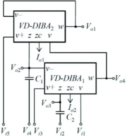
The filter from Fig. 2 can be generalized as shown in Fig. 6, considering five voltage inputs Vi1 to Vi5 and two
current outputs Io1 and Io2, the latter being added via a
“z-copy” technique [3]. The types of filter sections, corre-sponding to input-output pairs, are summarized in Tab. 1. The highlighted three items on the first line denoted “Vi1”
describe the features of the original filter from Fig. 2.
Fig. 6. Multi-input multi-output generalization of filter from
Fig. 2. Vo1 Vo2 Vo3 Vo4 Io1 Io2 Vi1 HP -BP LP -HP(2) -BP(4) Vi2 -HP BP HP(2) -BP(4) Vi3 -BP(1) LP BP(3) Vi4 HP -BP(1) -BP(1) -HP(4) Vi5 BP -LP -LP HP(2) -BP(4) Vi1=Vi3=Vi4 AP Vi3=Vi4 BR (1) BP gain is g m2C1/(gm1C2), (2) HP gain is gm1, (3) BP gain is gm2C1/C2, (4) BP (HP) gain is g
m2; otherwise, the gains are equal to one.
Tab. 1. Low-pass (LP), band-pass (BP), high-pass (HP),
all-pass (AP) and band-reject (BR) sections of multi-input multi-output filter in Fig. 6.
Note that particularly the column “Vo2” represents
a promising extension of the biquad features: utilizing the output Vo2, all basic filter types can be implemented via
a proper selection of the inputs, including allpass and band-reject sections (by interconnecting three or two inputs).
The additional current outputs of the internal OTAs of VD-DIBA No. 1 and 2 can easily serve as current outputs of BP and HP sections, enabling economical extension of the filter operation to the transconductance mode.
In the necessity of providing buffered, thus true
volt-age-mode HP, BP or LP outputs, one can use Vo1 or Vo4
terminals. For the operations when the input Vi1 is not used,
the feedback loop to the v terminal of VD-DIBA No. 2 should be led not from w but from z terminal of VD-DIBA No. 1. Since the output buffer is no longer included in the feedback loop, the filter stability and high-frequency be-havior will be improved.
6.
Comparison with Previous SIMO
Voltage-Mode Filters
Literature survey shows that a lot of papers dealing with SIMO voltage-mode filter using various active building blocks have been published [12-30]. Considering the kinds of active elements, the filters in the above references employ: current feedback amplifier (CFA) [12], current conveyor (CCII) [13], [14], four terminal floating nullor (FTFN) and operational transconductance amplifier (OTA) [15], differential voltage current conveyor (DVCC) [16-19], differential different current conveyor (DDCC) [20-22], DDCC and OTA [23], OTA [24-26], differential difference current conveyor transconductance amplifier (DDCCTA) [27], [28], fully differential current conveyor (FDCCII) [29-31], DDCC and current controlled current conveyor (CCCII) [32].
The proposed circuit in Fig. 2 is compared with sev-eral SIMO voltage-mode filters from [12-32]. The results are shown in Tab. 2. It can be seen that it matches all the criteria in the best way among all other filters.
In addition to the above SIMO filters, the three-input single-output voltage-mode biquad utilizing one VDIBA (voltage differencing inverting buffered amplifier) [33], two capacitors, and one resistor has been published in [34] and also in [35]. Note that VDIBA differs from VD-DIBA by voltage inverter which replaces the differential-input buffer in VD-DIBA. The filter from [34], [35] pays a tax for employing only one active element: Electronic control is limited to one parameter, namely the transconductance of the VD-DIBA, thus the controlling range is smaller in comparison to (5), without any possibility not to disturb Q with tuning f0. Since the single output is not of
low-imped-ance nature, all the implemented filter types require addi-tional voltage buffering.
7.
Conclusions
The voltage-mode biquad filter has been presented in this contribution. The advantages of the proposed circuit are that: (i) it performs low-pass, high-pass, and band-pass, functions from the same simple circuit configuration; (ii) the quality factor and the pole frequency can be electro-nically controlled; (iii) the filter has high input impedance; (iv) the circuit uses only two VD-DIBAs, two grounded capacitors and no resistors, which is attractive for its IC implementation; (v) the functionality of the filter can be easily extended for providing all-pass and band-reject sec-
Ref Active elements No. of active elements
No. of R+C Electronic
control
Grounded
capacitors only High input impedance
[12] CFA 5 5+2 No Yes Yes
[13] CCII 3(cir.1), 4(cir.2) 6+2(cir.1), 7+2(cir.2)
No Yes No [14] CCII 4(cir.1&cir.2),
3(cir.3), 2(cir.4)
5+2 No Yes No
[15] FTFN & OTA 2 & 2 4+2 Yes Yes Yes
[16] DVCC 3 4+2 No Yes Yes [17] DVCC 3 3+2 No Yes Yes [18] DVCC 2 3+2 No Yes No [19] DVCC 1 2+3 No No Yes [20] DDCC 2 3+2 No Yes No [21] DDCC 2 3+2 No Yes No [22] DDCC 1 3+2 No Yes No
[23] DDCC & OTA 1 & 2 0+2 Yes Yes Yes
[24] OTA 5 0+2 Yes Yes Yes
[25] OTA 8 0+2 Yes Yes Yes
[26] OTA 4 0+2 Yes Yes Yes
[27] DDCCTA 2 2+2 Yes Yes Yes
[28] DDCCTA 3 0+2 Yes Yes Yes
[29] FDCCII 2 2+2 No Yes Yes
[30] FDCCII 1 3+2 No Yes No
[31] FDCCII 1 2+2 No Yes Yes
[32] DDCC & CCCII 1+1 1+2 Yes Yes Yes Proposed
filter VD-DIBA 2 0+2 Yes Yes Yes
Tab. 2. Comparison of various SIMO voltage-mode filters.
tions via selecting various types of voltage inputs; (vi) the filter topology provides a possibility of its flexible modifi-cation and development, depending on the user’s require-ments, for example towards the transconductance mode of the operation.
The error analysis reveals that parasitic low-frequency gains of BP and HP sections can be suppressed via select-ing the gmRz product as high as possible. As results from the experiments described in Section 4, VD-DIBA should be implemented with Rz high enough. Otherwise, gm must be designed too high, which results in large working ca-pacitances. Then the corresponding low impedance level is a source of several troubles, especially low dynamic range of the voltage signals. For IC implementation, designing VD-DIBA with extra-high z-terminal impedance is thus a prerequisite for constructing high-performance biquads.
Acknowledgements
Research described in this paper was financially sup-ported from the Faculty of Industrial Education, King
Mongkut’s Institute of Technology Ladkrabang (KMITL), Grant No. 2557-0203022; and from Project PRO-K217 of the University of Defense Brno.
References
[1] SEDRA, A. S., SMITH, K. C. Microelectronic Circuits. 3rd ed. Florida: Holt, Rinehart and Winston, 1991.
[2] IBRAHIM, M. A., MINAEI, S., KUNTMAN, H. A 22.5MHz current-mode KHN-biquad using differential voltage current conveyor and grounded passive elements. International Journal of Electronics and Communications (AEÜ), 2005, vol. 59, no. 5, p. 311–318.
[3] BIOLEK, D., SENANI, R., BIOLKOVÁ, V., KOLKA, Z. Active elements for analog signal processing, classification, review and new proposals. Radioengineering, 2008, vol. 17, no. 4, p. 15–32. [4] BIOLEK, D., BIOLKOVÁ, V. First-order voltage-mode all-pass
filter employing one active element and one grounded capacitor.
Analog Integrated Circuits and Signal Processing, 2009, vol. 65, no. 1, p. 123–129.
[5] PRASAD, D., BHASKAR, D. R., PUSHKAR, K. L. Realization of new electronically controllable grounded and floating simulated inductance circuits using voltage differencing differential input
buffered amplifiers. Active and Passive Electronic Components, 2011, vol. 2011, Article ID: 101432.
[6] PUSHKAR, K. L., BHASKAR, D. R., PRASAD, D. Voltage-mode universal biquad filter employing single voltage differencing differential input buffered amplifier. Circuits and Systems, 2013, vol. 4, p. 47–51.
[7] BIOLEK, D., BAJER, J., BIOLKOVÁ, V., KOLKA, Z.,
KUBÍ-ČEK, M. Z Copy - Controlled Gain - Current Differencing Buff-ered Amplifier and its applications. Int. Journal of Circuit Theory and Applications. 2011, vol. 39, no. 3, p. 257–274.
[8] MAX435/MAX436 Wideband Transconductance Amplifiers, MAXIM, 19-0042; Rev. 1; 4/93.
[9] AD8129/AD8130 Low Cost 270 MHz Differential Receiver Amplifiers, Analog Devices, 2005. Available at: www.analog.com.
[10] MAX435 Family Macromodels,
http://www.maximintegrated.com/design/tools/modeling-simulation/spice/operational-amplifiers/macro/MAX435.FAM [11] AD8130 SPICE Macro-Model
http://www.analog.com/en/specialty-amplifiers/differential-amplifiers/ad8130/products/mod-spice-models/resources.html [12] ABUELMA'ATTI, M. T., AL-ZAHER, H. A. New universal filter
with one input and five outputs using current-feedback amplifiers.
Analog Integrated Circuits and Signal Processing, 1998, vol. 16, p. 239–244.
[13] HORNG, J. W., HOU, C., L., CHANG, C. M., CHUNG, W. Y., WEI, H. Y. Voltage-mode universal biquadratic filter with one input and five outputs using MOCCIIs. Computers & Electrical Engineering, 2005, vol. 31, p. 190–202.
[14] HORNG, J. W., HOU, C., L., CHANG, C. M., CHUNG, W. Y. Voltage-mode universal biquadratic filter with one input and five outputs. Analog Integrated Circuits and Signal Processing, 2006, vol. 47, p. 73–83.
[15] KUMAR, K., PAL, K. Voltage-mode universal biquadratic filter using FTFN and OTA. Journal of Electrical and Electronics Engineering, 2009, vol. 9, no. 2, p. 1083–1087.
[16] HORNG, J. W., HOU, C. L., CHANG, C. M., CHOU, H. P., LIN, C. T. High input impedance voltage-mode universal biquadratic filter with one input and five outputs using current conveyors.
Circuits System Signal and Processing, 2006, vol. 25, no. 6, p. 767–777.
[17] MINAEI, S., YUCE, E. All-grounded passive elements voltage-mode DVCC-based universal filter. Circuits System Signal and Processing, 2010, vol. 29, p. 295–309.
[18] HORNG, J. W. Lossless inductance simulation and voltage-mode universal biquadratic filter with one input and five outputs using DVCCs. Analog Integrated Circuits and Signal Processing, 2010, vol. 62, p. 407–413.
[19] HORNG, J. W. Voltage-mode multifunction biquadratic filter employing single DVCC. International Journal of Electronics, 2012, vol. 99, no. 2, p. 153–162.
[20] CHEN, H. P. Universal voltage-mode filter using only plus-type DDCCs. Analog Integrated Circuits and Signal Processing, 2007, vol. 50, no. 2, p. 137–139.
[21] CHIU, W. Y., HORNG, J. W. Voltage-mode biquadratic filters with one input and five outputs using DDCCs. Indian Journal of Engineering and Materials Sciences, 2011, vol. 18, p. 97–101. [22] CHIU, W. Y., HORNG, J. W. Voltage-mode highpass, bandpass,
lowpass and notch biquadratic filters using single DDCC.
Radioengineering, 2012, vol. 21, no. 1, p. 297–303.
[23] LEE, W. T., LIAO, Y. Z. New voltage-mode high-pass, band-pass and low-pass filter using DDCC and OTAs. International Journal of Electronics and Communications (AEÜ), 2008, vol. 62, no. 9, p. 701–704.
[24] HORNG, J. W. Voltage-mode universal biquadratic filter with one input and five outputs using OTAs. International Journal of Electronics, 2002, vol. 89, p. 729–737.
[25] KUMNGERN, M., SUWANJAN, P., DEJHAN, K. Electronically tunable voltage-mode universal filter with single-input five-output using simple OTAs. International Journal of Electronics, 2013, vol. 100, no. 8, p. 1118–1133.
[26] KUMNGERN, M., DEJHAN, K. Voltage-mode low-pass, high-pass, band-pass biquad filter using simple CMOS OTAs. In
Proceedings of the IEEE International Instrumentation and Measurement Technology Conference. 2009, p. 924–927.
[27] CHANNUMSIN, O., PUKKALANUN, T., TANGSRIRAT, W. Voltage-mode universal filter with one input and five outputs using DDCCTAs and all-grounded passive components.
Microelectronics Journal, 2012, vol. 43, no. 8, p. 555–561. [28] TANGSRIRAT, W., CHANNUMSIN, O., PUKKALANUN, T.
Resistorless realization of electronically tunable voltage-mode SIFO-type universal filter. Microelectronics Journal, 2012, vol. 43, no. 8, p. 555–561.
[29] CHEN, H. P. Voltage-mode FDCCII-based universal filters.
International Journal of Electronics and Communications (AEÜ),
2008, vol. 62, no. 4, p. 320–323.
[30] LEE, C. N., CHANG, C. M. Single FDCCII-based mixed-mode biquad filter with eight outputs. International Journal of Electronics and Communications (AEÜ), 2009, vol. 63, p. 736 to 742.
[31] MAHESHWARI, S., MOHAN, J., CHAUHAN, D. S. Novel cas-cadable all-pass/notch filters using a single FDCCII and grounded capacitors. Circuits, Systems, and Signal Processing, 2011, vol. 30, no. 3, p. 643–654.
[32] MANEEWAN, S., SREEWIROTE, B., JAIKLA, W. Electronically tunable voltage-mode universal filter using DDCC and CCCII. In Proceedings of the International Conference on Circuits, System and Simulation. 2011, p. 322–326.
[33] HERENCSÁR, N., KOTON, J., MINAEI, S., YUCE, E., VRBA, K. Novel resistorless dual-output VM all-pass filter employing VDIBA. In Proceedings of the 7th International Conference on Electrical and Electronics Engineering–ELECO 2011. Bursa (Turkey), 2011, p. 72–74.
[34] HERENCSÁR, N., CICEKOGLU, O., ŠOTNER, R., KOTON, J., VRBA, K. New resistorless tunable voltage-mode universal filter using single VDIBA. Analog Integrated Circuits and Signal Processing, 2013, vol. 76, p. 251–260.
[35] PUSHKAR, K. L., BHASKAR, D. R., PRASAD, D. Voltage-mode new universal biquad filter configuration using a single VDIBA. Circuits Systems and Signal Processing, 2014, vol. 33, p. 275–285.
About Authors ...
Winai JAIKLA was born in Buriram, Thailand. He re-ceived the B. S. I. Ed. degree in Telecommunication Engi-neering from King Mongkut’s Institute of Technology Ladkrabang (KMITL), Thailand in 2002, M. Tech. Ed. in Electrical Technology and Ph.D. in Electrical Education from King Mongkut’s University of Technology North Bangkok (KMUTNB) in 2004 and 2010, respectively. From 2004 to 2011 he was with Electric and Electronic Program, Faculty of Industrial Technology, Suan Sunandha Rajabhat University, Bangkok, Thailand. He has been with the Department of Engineering Education, Faculty of In-dustrial Education, King Mongkut’s Institute of
Technol-ogy Ladkrabang, Bangkok, Thailand since 2012. His re-search interests include electronic communications, analog signal processing and analog integrated circuits. He is a member of ECTI, Thailand.
Dalibor BIOLEK received the M.Sc. degree in Electrical Engineering from the Brno University of Technology, Czech Republic, in 1983, and the Ph.D. degree in Elec-tronics from the Military Academy Brno, Czech Republic, in 1989, focusing in algorithms of the symbolic and nu-merical computer analysis of electronic circuits with a view to the linear continuous-time and switched filters. He is currently with the Department of EE, University of De-fense Brno (UDB), and with the Department of Microelec-tronics, Brno University of Technology (BUT), Czech Republic. His scientific activity is directed to the areas of general circuit theory, frequency filters, and computer simulation of electronic systems. He has published over 300 papers and is author of three books on circuit analysis and simulation. At present, he is professor at the BUT and UDB in the field of Theoretical Electrical Engineering. Prof. Biolek is a member of the CAS/COM Czech National
Group of IEEE. He is also the president of Commission C of the URSI National Committee for the Czech Republic.
Surapong SIRIPONGDEE received the B. S. I. Ed. degree in Electronics and Computer and the M. Tech. Ed. electrical communications engineering from King Mongkut’s Institute of Technology Ladkrabang (KMITL), Thailand in 1997 and 2002, respectively. He has been with the Department of Engineering Education, Faculty of Industrial Education, King Mongkut’s Institute of Technol-ogy Ladkrabang, Bangkok, Thailand since 1997. His re-search interests include electronic communications, analog signal processing and analog integrated circuits.
Josef BAJER was born in 1982. In 2005, 2008, and 2011 he received the B.Sc. degree in Electrical and Special Air-craft Equipment, the M.Sc. degree in Avionic Systems, and Ph.D. degree in Electronic Systems at the Faculty of Mili-tary Technologies, University of Defense Brno (UDB), Czech Republic. His interests include analog and digital signal processing and applications of modern active ele-ments working in current and hybrid modes.