Design and Implementation of a High Power Dual-module
Parallel Charging System
Yu-En Wu
National Kaohsiung First University of Science and Technology, University Road, Yuanchau, Kaohsiung 824, Taiwan *Corresponding Author: [email protected]
Copyright © 2014 Horizon Research Publishing All rights reserved.
Abstract
This paper presents a high-power dual-module parallel charging system which consists of a power converter and digital control software. The power converter consists of an active power factor correction (APFC) circuit and a resonant voltage fed full-bridge converter (RVFFBC). The APFC circuit is used for AC/ DC conversion and power factor correction for improved power quality. The RVFFBC is used to provide stable power for charging the battery by converting the high voltage of the power stage to a lower value. The system software was designed by combining the power control loop into a voltage and current loop to achieve current sharing of the dual-module charging system and to overcome the effect of differences in hardware components. Finally, this paper demonstrates the implementation of a high-power dual-module charging system with a widely varying AC input voltage ranging from 85 ~ 265 Vac. Experimental results verified that the maximum power factor of the system and the Total Harmonic Distortion (THD) were 0.99 and 2.8% respectively. The proposed charging system possesses very high expansibility. The parallel dual-module output DC current of the system is 70 A and the total output power is 4 kW.Keywords
Active Power Factor Correction, Full-Bridge Converter, Parallel Charging System, THD1. Introduction
With the increase in the use of devices such as laptops, mobile phones, tablet PCs, etc., lithium batteries have gradually replaced lead-acid batteries as the power source of choice. Similarly, with the increase in the demand of battery capacity for use in applications such as electric vehicles (EV) and uninterruptible power systems (UPS), the characteristics of the charging systems of these batteries have assumed great importance [1]-[4], with a great deal of work being carried out in this area. The desired features of a good charging system are an improved power factor and low harmonic pollution.
Traditional AC-DC converters consist of a bridge rectifier and a filter capacitor. The advantages of such converters are
simplicity of the circuit structure and ease of control. However, they exhibit serious nonlinear distortion, which not only causes the power factor to be reduced, but also affects the device and power network equipment. It also affects the quality of the overall electrical supply system. This leads to poor power grid stability and power loss. Therefore, a power factor correction (PFC) circuit is generally used to improve these problems. The PFC circuit can be divided into two: active power factor correction (APFC) circuits and passive power factor correction (PPFC) circuits [5]-[7]. The correction capability of PPFC circuits is low and they are unable to meet standard requirements. APFC circuits use the Pulse Width Modulation (PWM) scheme, which leads to the input current and voltage waveforms having approximately the same phase. APFC circuits therefore meet the standard requirements and specifications. Current APFC circuits can achieve power factors in the range of 0.98~1, which enhances the power conversion efficiency and power quality of high-power high-current charging systems.
Typical charging systems which provide stable power source is designed by DC / DC converter circuit, it convert a high DC voltage to a low DC voltage in order to match the voltage of the battery pack. Commonly-used step-down DC/DC converter circuits such as buck, buck-boost, etc., suffer from the inherent disadvantages of having large current ripples and low output powers. To overcome these deficiencies, a full bridge converter circuit with a center tap rectifier filter circuit is proposed in this paper. Such a circuit has a highly stable output voltage and current.
2. Charging System Architecture
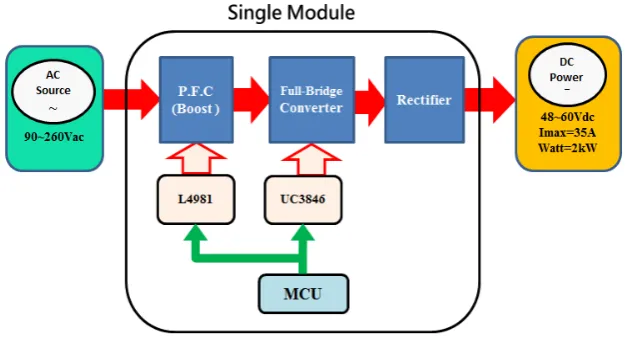
Fig. 1 shows the proposed single module charging system architecture. It can be divided into three parts. The first is the APFC circuit [14],[15] which is used to improve the power quality. The second is the RVFFBC which is used to provide stable power for charging the power battery. The third is a rectifier filter circuit with a center tap [16]-[18]. The PWM signal is generated by the microcontroller and the D/A converter circuit is used to convert the MCU signals to control the output current of the UC3846 IC. Each part will be illustrated in the following sub-sections.
2.1. Active Power Factor Correction (APFC)
[image:2.595.150.466.249.422.2]A commonly-used PFC circuit architecture includes a buck, buck-boost, boost, SEPIC converters, etc. Table 1 gives a comparison of the features of various converters. To meet the specifications of the proposed single module charging system, the Boost converter was used, as shown in Fig. 2. The IC L4981 was used to control the boost converter to achieve a power factor of about 0.99 with a widely varying AC input voltage (85Vac-265 Vac). The PFC circuit can operate in the continuous conduction mode (CCM) and can be used in charging systems of up to 500 W.
[image:2.595.111.498.467.741.2]Figure 1. Single module charging system architecture.
Table 1. A comparison of the features of various converters.
Buck Boost Buck- Boost SEPIC VO Polarity Positive Positive Negative Positive
Crossover
Distortion Yes No No No Number of components Less Less Less More
PFC Low Highest Low High
Figure 2. Architecture of APFC.
L
C
D
+
─
Vac S
iL Bridge
rectifier
PFC Circuit
+ Vi
-L4981
5.1V
mul S
R Q
cmp
R1
R2
R1
Iac
R4 R6
R5 R7
R8
OSC
Isence Vfeed
GDRV
2.2. Resonant Voltage Fed Full Bridge Converter (RVFFBC)
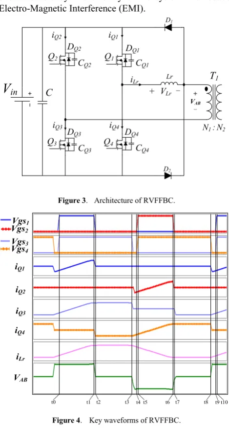
[image:3.595.58.293.179.638.2]The architecture of the RVFFBC is shown in Fig. 3. The resonance is generated by the resonant transformer, the inductor Lr, and the parasitic capacitor of the power switches. Thus, zero voltage switching (ZVS) of the power switches is achieved as shown in Fig. 4. It also greatly improves the overall efficiency and stability of the system and reduces Electro-Magnetic Interference (EMI).
Figure 3. Architecture of RVFFBC.
Figure 4. Key waveforms of RVFFBC.
The operation of the RVFFBC is divided into positive and negative half-cycles. As the operation is similar in each half-cycle, only the positive half-cycle is described in this paper. The positive half-cycle operation mode is divided into five intervals t0 – t5 as shown in Fig. 5. The operation first enters the energy clamping stage, and then enters the Mode 1 ~Mode 5 interval operation, it is illustrated as follows. Energy clamping interval
This interval is shown in Fig. 5(a), which is used to improve the energy imbalance between the resonant inductor and the transformer. Clamping diodes D1 and D2 improve the oscillation generated by the reverse recovery time of the rectifier diode and stabilizes the unstable energy state between the transformer and the resonant inductor Lr. Mode 1: Energy transfer interval [t0-t1]
The switches Q1 and Q3 are turned on as shown in Fig.
5(b). Vin is equal to the sum of the inductor voltage VLr and
the transformer's primary voltage VAB. The input current
flows from switch Q1 to Q3 and energy is transferred to the
transformer and the resonant inductor Lr. Mode 2: Resonant state interval [t1-t2]
The switch Q3 is kept in the on-state and Q1 is turned off,
as shown in Fig. 5(c). The current direction is the same as in Mode 1. The parasitic capacitor CQ1 of Q1 is charged and
the parasitic capacitor CQ4 of Q4 is discharged. Therefore,
the voltage across Q4 is reduced.
Mode 3: Energy hold interval [t2-t3]
The inductor Lr releases energy and the switch Q3 is
kept in the on state, as shown in Fig. (d). After the discharge of CQ4 to turn on DQ4, the voltage across Q4 is reduced.
Thus, Q4 is turned on under ZVS.
Mode 4: Resonant state interval [t3-t4]
The switch Q4 is kept in the on-state, as shown in Fig.
5(e). The resonant effect is generated by the resonant inductor and the parasitic capacitor of CQ3 and CQ2. The
switch Q2 is turned on under ZVS at this moment.
Mode 5: Energy transfer interval [t4-t5]
The switches Q2 and Q4 achieve ZVS under the resonant
effect, and the current flow direction is from Q2 to Q4. The
positive half cycle operation is over and the device enters the negative half-cycle at this time, as shown in Fig. 5(f). Q2
iLr Lr
V
in CD1
D2
+ VAB
-N1 :N2
T1
Q3 Q4 C
Q4 DQ4 CQ1 DQ1 DQ3 CQ3 DQ2
CQ2 Q1
iQ1
iQ2
iQ4
iQ3
+ VLr
-t2 t3 t4 t5
Vgs1 Vgs3 Vgs4 Vgs2 iQ1 iQ2 iQ3 iQ4 iLr VAB
Q2
iLr Lr
Vin C
D1
D2
+ VAB
-N1 :N2
T1
Q3 Q4 C
Q4 DQ4 CQ1 DQ1 DQ3 CQ3 DQ2
CQ2 Q1
iQ1
iQ2
iQ4
iQ3
+ VLr
-Q2
Lr
Vin C
D1
D2
+ VAB
-N1 :N2
T1
Q3 Q4 C
Q4 DQ4 CQ1 DQ1 DQ3 CQ3 DQ2
CQ2 Q1
iQ1
iQ2
iQ4
iQ3
+ VLr
-iLr
(a) Energy clamping interval (b) Mode 1
Q2
Lr Vin C
D1
D2
+ VAB
-N1 :N2
T1
Q3 Q4 C Q4 DQ4 CQ1 DQ1 DQ3 CQ3 DQ2
CQ2 Q1
iQ1
iQ2
iQ4
iQ3
+ VLr
-iLr
Q2
iLr Lr
Vin C
D1
D2
+ VAB
-N1 :N2
T1
Q3 Q4 C Q4 DQ4 CQ1 DQ1 DQ3 CQ3 DQ2
CQ2 Q1
iQ1
iQ2
iQ4
iQ3
+ VLr
-(c) Mode 2 (d)Mode 3
Q2
iLr Lr
Vin C
D1
D2
N1 :N2
T1
Q3 Q4 C
Q4 DQ4 CQ1 DQ1 DQ3 CQ3 DQ2
CQ2 Q1
iQ1
iQ2
iQ4
iQ3
+ VLr - + VAB
-Q2
iLr Lr
Vin C
D1
D2
N1 :N2
T1
Q3 Q4 C
Q4 DQ4 CQ1 DQ1 DQ3 CQ3 DQ2
CQ2 Q1
iQ1
iQ2
iQ4
iQ3
+ VLr - + VAB
[image:4.595.93.521.85.601.2]-(e)Mode 4 (f) Mode 5
Figure 5. RVFFBC operating mode under the positive half cycle.
[image:4.595.314.545.639.717.2]2.3. Rectifier Filter Circuit
Fig. 6 shows the rectifier and filter circuit with the center tap transformer double winding, which provides the positive and negative half-cycles. Therefore, the output current ripple has a frequency which is twice that of the switching frequency of the power switches. This results in a stable DC
output voltage and a small current ripple. N1 :N2
T
1 D2 L C + VO - + VTH - + VTL -+ VL -
IL IO
D1
ID1
ID2
2.4. Parallel Operation of Dual-module Charging System The proposed architecture of the dual-module charging system is shown in Fig. 7. To achieve current sharing, the master microcontroller outputs a reference current to adjust the output of the other module. Thus, the parallel operation dual module charging system is implemented by the current sharing scheme, and its control block is shown in Fig. 8. The
outer loop is the feedback voltage Vbat that regulates the
output voltage and the inner loop is the feedback current Iout
that improves the dynamic response. In addition, the output power loop, which is generated by the product of the feedback voltage and current, is used to establish the common reference power Pref for achieving the same output
power of each module. Fig. 8 shows the hardware of the dual-module charging system.
AC Source
Battery pack
APFC RVFFBC filter circuitRectifier
MCU L4981 UC3846
Iref
Slave Master
APFC RVFFBC filter circuitRectifier
[image:5.595.145.465.184.373.2]MCU L4981 UC3846
Figure 7. Dual-module charging system architecture.
PID PID PWM
Vref Iref
DA Converter
╳
+
-
╳
+ -
╳
+ -
Iout
Micro Control Unit
Current Loop Voltage Loop
Vbat
-
Pref UC3846
Power Loop
Voltage loop Current Loop
[image:5.595.140.492.405.556.2]Start
Watch Dog
NO
Yes
Flag_A/D=1
A/D Value conversion
Flag_Protection =1
Flag_chargemode =1 Sub_Protection
Sub_Chargemode
Sub_ Constant Charge Power
Return
Yes
Yes
NO
[image:6.595.151.461.76.544.2]NO
Figure 9. System program flowchart.
3. System Program
Fig. 9 shows a system program flowchart which contains the following three subroutines: the charge mode program, the protection program, and the constant charge power program. These are explained as follows.
3.1. Charge Mode Program
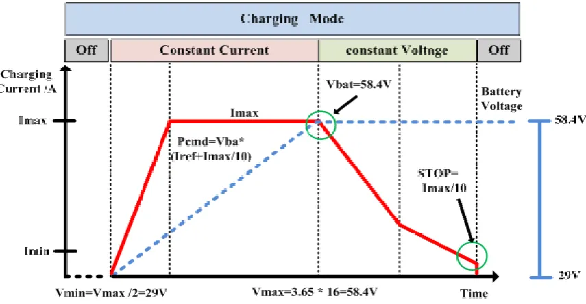
Table 2 shows the charging/discharging specification of the battery cell. It can be seen that the charging method of the battery cell is constant voltage-constant current (CV-CC), and the battery cell’s maximum charging current and voltage were 3 A and 3.65 V, respectively. The charging voltage of the charging system must be determined according to the battery cell’s charging curve, as shown in
[image:6.595.311.552.628.756.2]Fig. 10.Therefore, 16 battery cells were connected in series to constitute a battery pack whose maximum charging voltage was 58.4 V.
Table 2. The charging/discharging specification of the battery cell. Operation Conditions
Charging Voltage 3.65 V Charging Method CC-CV Cut-off Discharge Voltage 2.10 V Max. Continuous Discharge Current 10 A
Max. Charge Current 3 A Operating Temperature
Range
Discharge -10 ~ 55 oC
Figure 10. Charging curve of the charging system.
The charging procedure consists of three steps which are explained below.
1. Battery Low Voltage Detection
Fig. 11 shows a flowchart of the charging mode program. First, it is determined whether the battery voltage is > 29V. If it is, then the battery may bedamaged or the wiring may be abnormal. The output powercommand(Pcmd)must be setto low. If the battery voltage is < 29V, it represents that the battery can be charged properly.
2. Constant Current: CC
The initial value of the output current is 0, and considering the battery capacity, the output power command (Pcmd) which according to the 1/10 setting value of maximum current (Imax) gradually increase, it can ensure the output current of different battery capacity sets the value of the maximum current to 1/10 of its value to ensure that
the output current matches the capacity of a different battery. When the output power command (Pcmd) increases to the maximum current (Imax), the charging system output current (Iref) corresponds to the maximum output current command (Imax). This value is maintained until the battery voltage reaches 58.4 V. Then, the charging mode changes.
3. Constant Voltage: CV
Vbat < 29V
Battery Charge mode
No Yes
Vbat < 58.4V
No
Inow ≧ Imax/3
Pcmd=0
Return
Inow = Imax Yes
Yes
Vbat = 58.4V
Pcmd=Vbat.(Inow- Imax/3) Yes
No
Yes
Yes No
No
Inow ≧Imax/10 No
Yes
No
Pcmd=Vbat .(Inow+ Imax/10)
[image:8.595.103.509.73.543.2]Pcmd=Vbat.(Inow - Imax/10)
Vac=90~250Vac
Vbat=29~58.4V
Charger Temperature
≦80℃
Relay_ON
Return
Start
Relay_OFF No
Yes
Yes
Yes
No
No
Iset > 0 No Yes
Figure 12. Protection program flowchart.
3.2. Protection Program
Fig. 12 shows a flowchart of the protection program. It can be seen that the protection items of the charging system include input voltage, battery voltage, charger temperature, and charge current.
3.3. Constant Charge Power Program
Constant power control possesses the function of limiting the maximum value of the system power; its output control is to change the rating of the current regulator. Such a control scheme can achieve a fast response of the DC current regulation loop. In addition, it can also substantially prevent transients and fluctuations generated by the severe variation of the feedback circuit.
Fig. 13 shows a flowchart of the constant charge power program which consists of three protection functions. First, consider the security protection. When the instantaneous output exception occurs, that is, when the product of battery
voltage Vbat and output current Iout is greater than the constant power, it must be immediately determined whether the battery voltage is > 58.4Vor <29V. If it does, the output power command Pcmd is immediately set to 0. This avoids charging the system by overcurrent caused by a short circuit. The maximum temperature protection is called the drop power function. We must detect whether the current temperature Tnow reaches the over-temperature; the temperature must reach 70°C before entering the computing equation, and the maximum temperature Tmax is designed to be 80°C; if it does, it means that the temperature of the charging system is higher than 70°C. The charging system is turned off when the temperature reaches 80°C.
[image:9.595.201.409.74.487.2]Start
Charge Temperature >70℃ Yes
NO
Vbat.Inext >Pmax
Pcmd=Pmax Yes
NO Pnow > Pmax
Calculation Vbat.Inow=Pnow
Vbat ≧ 58.4V Yes
Pcmd =0 Yes
NO
Vbat ≦ 29V
NO Pcmd=Pmax
Return
Yes Charge Temperature
>80℃
Pcmd=Pmax(Tmax-Tnow) Pcmd =0 Yes NO
[image:10.808.138.676.72.481.2]NO
4. Experimental Results and Discussions
Table 3. System components and electrical specifications. Boost RVFFBC L / Lr 0.53 mH 10 uH Diode DSEP30-06B Mur3020pt MOSFET 24N60C3 P25NM50N
Single-module Dual-module Input Voltage 90-260 Vac 90-260 Vac Output Voltage 48-60 Vdc 48-60 Vdc
Max. Current 35 A 70 A Output Wattage 2 kW 4 kW
In this paper, a dual-module charging system using a parallel architecture with a digital microcontroller
P89LPC938 is implemented. Its maximum output current is 70 A and the output power is 4 kW. Table 3 shows the system’s electrical specifications and component specifications.
4.1. Single Module Verification
This section starts by testing the effectiveness of a single-module. Fig. 14(a)–(d) shows the input and output measured waveforms operating under a light load and a full load, respectively. The light load input power was 336.7 W and the output power was 290.1 W. The full load input power was 2096.2 W and the output power was 1904 W. Fig. 15 shows the efficiency curve of the single module under different operating powers. It can be seen that the highest efficiency was 89.7% and the full load efficiency was 89%.
v
aci
acI
dcV
dc(vac: 200V/div , iac:5.0A/div , time: 5.0ms/div) (Vdc: 50V/div , Idc: 5.0A/div , time: 10.0ms/div)
(a)Input waveform under light load (b)Output waveform under light load
(vac: 200V/div , iac: 10.0A/div , time: 5.0ms/div) (Vdc: 50V/div , Idc: 10.0A/div , time: 10.0ms/div)
(c)Input waveform under full load (d)Output waveform under full load
[image:11.595.86.528.283.656.2]Figure 15. Efficiency curve of a single module.
4.2. Current Sharing of Dual-Module Measurement
Fig. 16 shows that the total output current under light load was 10 A and that the current error was 0.2 A. Fig. 17 shows that the total output current under full load was 70 A, and that the current error was 0.4 A. Fig. 18 shows the current error comparison of the dual-module under different operating powers. It can be seen that the proposed dual module charging system exhibits good current sharing behavior.
[image:12.595.184.425.350.516.2](Ia: 2.0A/div ; Ib: 2.0A/div ; time: 10.0ms/div)
Figure 16. Measured output current of dual module under light load (10 A).
[image:12.595.183.426.547.707.2](Ia: 20.0A/div ; Ib: 20.0A/div ; time: 10.0ms/div)
Figure 18. Current error comparison of dual module charging system.
(vac:250V/div ; iac:10.0A/div ; time:5.0ms/div)
(a)Input voltage and current
[image:13.595.58.299.303.463.2](b) Output voltage and current
Figure 19. The input/output voltage and current of a single module.
(vac:250V/div ; iac:10.0A/div ; time:5.0ms/div) (a) Input voltage and current
(b) Output voltage and current
[image:13.595.322.548.307.452.2]0 0.5 1 1.5 2 2.5
3 5 7 9 11 13 15
IEC6100-3-2 Single Module Dual Module
Harmonic Current
(A
)
[image:14.595.99.509.74.489.2]Harmonic Level (n)
Figure 21. IEC61000-3-2 odd harmonics.
Figure 22. Measured result of the charging curve of a single module.
4.3. Power Factor and THD Measurement
[image:14.595.100.513.77.269.2]Fig. 19 shows the input/output voltage and current of a single module. It can be seen that the output voltage and current were 53.7 V and 34.3 A, respectively. Fig. 20 shows the input/output voltage and current of a dual module where it can be seen that the output voltage and current were 54.4 V and 70.3 A, respectively. Table 4 shows that the measured PF and THD values of the single-module were 0.98 and 3.3%, respectively, and that those of the dual module were 0.99 and 2.8%, respectively. In addition, Fig. 21 shows odd harmonics. It can be seen that the proposed charging system meets the requirements of the IEC61000-3-2 standard.
Table 4. Measured PF and THD values for single-module and dual-module.
PF Value THD Single-module 0.98 3.3% Dual-module 0.99 2.8%
4.4. Charging Curve Verification
[image:14.595.57.297.690.744.2]The charging curve of a battery cell is shown in Fig. 10. The first stage is CC charging mode in which the charging system charges the battery pack with a maximum charge current of Idc=35 A. When the battery voltage was gradually increased to 58.4 V, the charging system switched to the second stage which is the CV charging mode. When the charging current gradually decreased, the battery voltage maintained a maximum voltage of 58.4 V. When the charge current dropped to zero, the charging system was shut down.
Figure 23. Measured result of the charging curve of a dual module.
5. Conclusions
In this paper, a dual module parallel charging system is presented, which can be used for AC voltages varying from 85 V to 265 V. The maximum PF was 0.99, the THD was 2.8%, and the specifications are consistent with the requirements of the IEC61000-3-2 standard. The RVFFBC significantly improves the overall efficiency, system stability, and EMI. The dual module charging system can achieve a maximum output current of 70 A, and its current error is less than 2%. The proposed charging system has a high expansibility and utility and is suited for the requirements of high power charging.
REFERENCES
M. J. Isaacson, M. E. Daman, R. P. Hollandsworth, “Li-ion [1]
batteries for space applications,” Energy Conversion Engineering Conference, 1997, pp. 31-34.
T. Yanagihara, A. Kawamura, “Residual capacity estimation [2]
of sealed lead-acid batteries for electric vehicles,” Power Conversion Conference, 1997, Vol. 2, pp. 943-946.
J. M. Hawkins, “Some field experience with battery [3]
impedance measurement as a useful maintenance tool,”
Telecommunications Energy Conference, 2006, Vol. 21, NO.5, pp. 263-269.
L. M. Hofland, E. J. Stofel and P. K. Taenaka, “Galileo [4]
probe Li-SO2 battery cell life testing,” IEEE Aerosp.
Electron. Syst., 1996, pp. 14-18.
J. P. Gegner, C. Q. Lee, “Linear Peak Current Mode Control: [5]
A Simple Active Po-wer Factor Correction Control Technique for Continuous Conduction Mode,” IEEE International Conference on Power Electronics Specialists, 1996, pp.196-202.
J. Luo, M. K. Jeoh, and H. C. Huang, “A New Continuous [6]
Conduction Mode PFC IC with Average Current Mode Control,” IEEE International Conference on Power Electronics and Drive Systems, 2003, pp. 1110-1114. M. Ferdowsi, and A. Emadi, “Estimative Current Mode [7]
Control Technique for DC-DC Converters Operating in Discontinuous Conduction Mode,” IEEE International
Conference on Power Electronics Letters, 2004, pp. 20-23. Yuehui Huang, Student Member, “Circuit Theoretic [8]
Classification of Parallel Connected DC-DC Converters,"
IEEE Transactions on Circuits and Systems, 2007, Vol. 54, NO.5.
S. Luo, Z. Ye, R. Lin and F. C. Lee, “A Classification and [9]
Evaluation of Parallel Methods for Power Supply Modules,”
CPES Seminar’98, 1998, pp. 221-231.
C. S. Lin and C. L. Chen, “Single-wire current-share [10]
paralleling of Current-mode-controlled DC power supplies,”
IEEE Trans. On Industrial Electronics, 2000, pp.780-786. Y. Panov and M. M. Jovanovic, “Design considerations for [11]
12-V/1.5-V, 50-A Voltage regulator modules,” IEEE Trans. Power Electron. , 2001, Vol. 16, NO.6.
E. J. Bueno, A. Hernandez, F. J. Rodriguez, C. Giron, R. [12]
Mateos, and S. Cobreces, “A DSP- and FPGA-Based industrial control with high-speed communication interfaces for grid converters applied to distributed power generation systems,” IEEE Trans. Power Electron. , 2009, Vol.56, NO.3, pp. 654-669.
Tsai-Fu Wu, Yu-En Wu, Hui-Ming Hsieh, “Current [13]
Weighting Distribution Control Strategy for Multi-Inverter Systems to Achieve Current Sharing,” IEEE Transactions on Power Electronics, 2007, Vol. 22, NO.1, pp. 160-168. High Power-Factor Preregulator Data Sheet, Unitrode [14]
Integrated Circuits, 1992.
Unitrode Integrated Circuits Enhanced High Power Factor [15]
B.R. Lin, K. Huang and D. Wang, “Analysis and [16]
implementation of full-bridge converter with current double rectifier,” IEEE Electronics. Power Applications, 2005, Vol. 152, No. 5.
C. Iannello, S. Luo and I. Batarseh, “Full Bridge ZCS PWM [17]
Converter for High-Voltage High-Power Applications,”
IEEE Trans. Power Electronics, 2002, Vol. 38, No. 2, pp. 515-525.
Y. Song, P. N. Enjeti, “A New Soft Switching Technique for [18]
Bi-Directional Power Flow, Full-bridge DC-DC Converter, ”
Conference Record of the Industry Applications Conference, 37th LAS Annual Meeting, 2002, Vol.4, pp. 2314-2319.
Yuri Panov, Milan M. Jovanovic, “Loop Gain Measurement [19]
of Paralleled DC-DC Converters with Average-Current-Sharing Control,” IEEE Transactions on Power Electronics, 2008, Vol. 23, NO.6, pp. 2942-2948. Yuehui Huang, Student Member, “Circuit Theoretic [20]
Classification of Parallel Connected DC-DC Converters, "IEEE Transactions on Circuits and Systems,
2007, Vol. 54, NO.5.
S. Luo, Z. Ye, R. Lin and F. C. Lee, “A Classification and [21]
Evaluation of Parallel Methods for Power Supply Modules,”
CPES Seminar’98, 1998, pp. 221-231.
C. S. Lin and C. L. Chen, “Single-wire current-share [22]
paralleling of Current-mode-controlled DC power supplies,”
IEEE Trans. On Industrial Electronics, 2000, pp.780-786. Y. Panov and M. M. Jovanovic, “Design considerations for [23]
12-V/1.5-V, 50-A Voltage regulator modules,” IEEE Trans. Power Electron. , 2001, Vol. 16, NO.6.
T. Ikeya etc., “Multi-Step Constant-Current Charging Method [24]
for an Electric Vehicle Nickel/Metal Hydride Battery with High-Energy Efficiency and Long Cycle Life,” Journal of Power Sources, March 2002, Vol. 105, No. 1, pp. 6-12. C.H. Lin and C.Y. Hsieh, “A Li-ion battery charger with [25]
smooth control circuit and built-in resistance compensator for achieving stable and fast charging,” IEEE Transactions on Circuits and Systems , 2010, Vol. 57, NO.2, pp. 506-517. Min Chen, Gabriel A. Rincin Mora, “Accurate, Compact, [26]
and Power-Efficient Li-Ion Battery Charger Circuit,” IEEE Transactions on Circuits and Systems, 2006, Vol. 53, NO.11, pp. 1180-1184.
C. Iannello, S. Luo and I. Batarseh, “Full Bridge ZCS PWM [27]
Converter for High-Voltage High-Power Applications,”
IEEE Trans. Power Electronics, 2002, Vol. 38, No. 2, pp. 515-525.
K. C. Tseng, T. J. Liang, “Novel high-efficiency step-up [28]