U N I V E R S I T E DE
GRENOBL^E
Pour obtenir le grade de
DOCTEUR DE L'UNIVERSITE DE GRENOBLE
Specialite : Nano-Electronique et Nano-TechnologiesArrete ministeriel : 7 aoirt 2006
((
Mohamad Hairol I JABBAR
>>
These dirigee par cc Dominique 1 Houzet >>
codirigee par cc Omar 1 Hammami >>
preparee au sein du Laboratoire G I P S A ~ L ~ ~ , Grenoble and ENSTA ParisTech, Paris
dans ~ ' ~ c o l e Doctorale EEATS
Methodologies- de Conception
ASIC Pour des Systemes sur
Puce
3D
Heterogenes
a
Base
de Reseaux sur Puce
3D
These soutenue publiquement le cc 21/03/2013 *,
devant le jury compose de :
M. Ian 0 Connor
Professeur, Ecole Centrale de Lyon, France, President, Rapporteur
.
Paul Franzonofesseur, North Carolina State University, ~ t a t s - ~ n i s , Rapporteur
.
Said HamdiouiABSTRACT
For many years, Moore's Law has been the primary driving force enabling the evolution of
semiconductor industry with the ability to double the transistor count on a silicon die for every two
years. However, shrinking transistor dimensions, also known as CMOS scaling to be able to design
and manufacture higher performance devices has become much more difficult than it is previously
as we are approaching very deep submicron technologies such as 20 nm and beyond. The issues of
design complexity and the exponential increase of cost to manufacture devices based on these very
deep submicron technologies are among the great hurdles currently being faced by the industry
making it unattractive performance per cost solution. The transition to 450 mm (18") wafer to help
reducing manufacturing cost for advanced process technology and the development of extreme
ultraviolet (EUV) lithography tools are also facing technical difficulties that remain to be solved in
the next several years while at the same time requires multi billion dollar investment to build new
manufacturing facilities as well as new processing equipments.
3D integration has been around since decades ago but only now the industry is paying great
attention to this technology as a result of economical and technical difficulties that arise from the /
transistor shrinking in 2D technology. It has been the,subject of' extensive research in the industry
and academia due to benefits it could potentially offer such as higher performance, lower power
consumption, larger memory bandwidth, small form factor and support for heterogeneous
technology integration making it suitable for several application domains particularly in mobile
devices. 3D technology could provide higher memory bandwidth through its excessive vertical
connections using TSV or microbumps as in wide I/0 memory architecture and can also
accomodate high memory capacity when using memory-on-logic or memory-on-memory stacking.
Shorter vertical interconnection between stacked dies or wafers as well as reduction of horizontal
wirelength due to stacking will eventually provide higher performance per watt. However, there are
also some challenges that exist in 3D technology and they have to be solved before it can be widely
adopted as a mainstream technology for high volume production such as high temperature effect,
testing of 3D architecture and most importantly for the designers is 3D design tools, specifically the
tools that are capable of doing 3D synthesis, 3D place and route as well as 3D optimization at each
step.
With the recent trend of mainstream multipr~cessor technology that is moving towards increasing
the number of processing cores to support higher performance applications, Network-on-Chip
(NoC) has become the primary technology in meeting the demand of high performance, scalability
and flexibility for processor's and Intellectual Property (IP) cores' communication. Works on
multiproce~sor and NoC architecture in 3D technology have been carried out for many years
covering various issues such as partitioning method and NoC topologies but most of the prior works
only consider software simulation for the performance analysis where the results is less accurate
and therefore cannot be truly used for evaluating the benefits bring by 3D technology. The need for
performance analysis from design implementation results is highly desirable to be able to make the
right conclusions regarding the potential benefits it offers. In this thesis, we study the 3D NoC
architectures through physical design implementations using real 3D technology being implemented
in the industry. Based on the routed netlists, we conduct performance analysis to evaluate the 4 :? '. benefit of 3D architecture compared with its 2D implementation. But firstly, we present ou$ initial
work designing and implementing a 2D NoC-based MPSoC architecture on FPGA intended to
identify design issues related to the 2D MPSoC design.
Based on the proposed 3D design flow focusing on timing verification by leveraging the benefit of
negligible delay of microbumps structure for vertical connections, we have conducted partitioning
techniques for 3D NoC-based MPSoC architecture including homogeneous and heterogeneous
stacking using Tezzaron 3D IC technlogy. Design and implementation trade-off in both partitioning
methods is investigated to have better insight about 3D architecture so that it can be exploited for
optimal performance. Using homogeneous 3D stacking approach, NoC architectures are explored to
identify the best topology between 2D and 3D topology for 3D MPSoC implementation. The
architectural explorations have also considered different process technologies highlighting the wire
delay effect to the 3D architecture performance especially for interconnect-dominated design.
Additionally, we performed heterogeneous 3D stacking of NoC-based MPSoC implementation with
GALS style approach and presented several physical designs related analyses regarding 3D MPSoC
design and implementation using 2D EDA tools.
-
Finally we conducted an exploration of 2D EDA tool on different 3D architecture to evaluate the
impact of 2D EDA tools on the 3D architecture performance. Since there is no commercialize 3D
design tool until now, the experiment is important on the basis that designing 3D architecture using
2D EDA tools does not have a strong and direct impact to the 3D architecture performance mainly
because the tools is dedicated for 2D architecture design. Integrating manual tools (scripts to
constraint the design) to the 2D EDA tools to design 3D architecture is the common method to
achieve performance benefit but this method loses the most important design step of 3D
Pendant de nombreuses annCes, la loi de Moore a CtC la principale force motrice permettant
1'Cvolution de l'industrie des semiconducteurs avec la possibilitC de doubler le nombre de transistors
sur une puce de silicium pour tous les deux ans. Toutefois, la diminution des dimensions des
transistors, appelCs aussi mise B 1'Cchelle CMOS pour Stre en mesure de concevoir et de fabriquer
des appareils plus performants est devenu beaucoup plus difficile qu'elle ne l'est dCjB que nous nous
approchons de technologies submicroniques profondes tels que 20 nm et au-delB. Les questions de
la complexit6 de la conception et de l'augmentation du coBt exponentiel pour la fabrication de
dispositifs bases sur ces technologies submicroniques profondes sont parmi les grands obstacles
actuellement rencontrks par l'industrie qui rend la performance peu attrayante pour solution
Cconomique. La transition & plaquette de 450 mm (18 ") pour aider B rCduire le coBt de fabrication
pour la technologie avancCe des processus et le dkveloppement d'outils de lithographie par
ultraviolets extrsme (EUV) sont Cgalement confrontCs B des difficult& techniques qui restent B
rbsoudre dans les prochaines annCes alors que dans le meme temps nCcessite investissements de
plusieurs milliards de dollars pour construire de nouvelles usines ainsi que des Cquipements de
traitement de nouvelles.
, /
L'intCgration 3D a CtC autour depuis des dCcennies auparavant, mais que maintenant l'industrie
accorde une grande attention B cette technologie en raison des difficultCs Cconomiques et techniques
proviennent du contraction du transistor dans la technologie 2 ~ . I1 a fait l'objet de recherches
approfondies dans l'industrie et le milieu universitaire en daison de certains avantages qu'elle
pourrait potentiellement offrir telles de meilleures performances, faible consommation d'energie, la
mtmoire de bande passante plus large, plus petit facteur de forme et de soutien pour llintCgration
des technologies hCtCrogknes ce qui conviknt pour plusieurs domaines d'application
particulikrement dans des appareils mobiles. La technologie 3D peut fournir une memoire de bande
passante plus ClevCe par l'intermtdiaire de ses connexions verticales excessives B l'aide TSV ou
microbilles selon Ifarchitecture de la memoire Cventail d'E/S et peut Cgalement accueillir une grande
capacitC de mCmoire pour l'utilisation de la mCmoire-B-mCmoire logique ou mCmoire-8-logique
d'empilement. Interconnexion verticale plus courte entre des matrices empilCes ou de plaquettes
ainsi que la reduction des longueur de fil horizontale due B l'empilement finira par offrir de
meilleures performances par watt. Cependant, il y a aussi des dCfis existent dans la technologie 3D,
et ils doivent stre rCsolus avant de pouvoir largement adopt6 comme une technologie majeure pour
la production de volume ClevC, cornrne l'effet de la temperature ClevCe, les tests &architecture 3D et
le plus important pour les concepteurs sont des outils de conception 3D, spkcifiquement les outils
qui sont capable de faire la synthkse 3D, le lieu et llitinCraire en 3D ainsi que l'optimisation 3D B
chaque &ape.
Avec la tendance rCcente, la technologie multiprocesseurse dCplace vers l'augmentation du nombre
de coeurs de traitement pour supporter les applications haute performance, rCseau sur une puce
(NoC) est devenue la principale technologie pour rCpondre B la demande des performances, une
CvolutivitC et une flexibilitC ClevCes pour le processeur et propriCtt intellectuelle (PI) de
communication de coeurs >>.Travaux de multiprocesseur et de l'architecture NoC dans la technologie
3D ont CtC rCalistes depuis de nombreuses annCes sur divers sujets tels que la mCthode de paqtage
4 f T (
de topologies NoC mais la plupart des travaux antkrieurs ne considkre pas le logiciel de simplation
pour l'analyse de la performance oii les rCsultats sont moins precis et ne peuvent donc pas Stre
vraiment utilisCes pour Cvaluer les btnCfices apporter par la technologie 3D. La nCcessit6 d'une
analyse de la performance des rCsultats de la mise en oeuvre de conception est fortement souhaitable
d'Stre en mesure de faire les bonnes conclusions quant aux avantages potentiels qu'ils peuvent offrir.
Dans cette thbse, nous Ctudions les architectures 3D NoC grgce B des implCmentations de
conception physiques en utilisant la technologie 3D rCel mis en oeuvre dans l'industrie. Sur la base
des listes d'interconnexions en dCroute, nous procCdons B l'analyse des performances dlCvaluer le
bCnCfice de l'architecture 3D par rapport B sa mise en oeuvre 2D. Mais tout d'abord, nous vous
prtsentons notre travail initial de conception et la mise en oeuvre d'un NoC 2D bas6 sur
l'architecture MPSoC sur FPGA pour but d'identifier les problkmes de conception lies B la
conception 2D MPSoC.
Sur la base du flux de conception 3D proposC en se concentrant sur la ~Crification temporelle en
s'appuyant sur llintCrSt de retard negligeable de la structure de microbilles pour les connexions
verticales, nous avons men6 des techniques de partitionnement de NoC 3D bas6 sur l'architecture
MPSoC y cclmpris empilement homogkne et hCtCrogkne en utilisant la technologie Tezzaron 3D IC.
La conception et la mise en oeuvre de compromis dans les deux mCthodes de partitionnement est
CtudiCe pour avoir un meilleur a p e r y sur l'architecture 3D de sorte qu'il peut Stre exploitCe pour des
performances optimales. En utilisant l'approche empilage 3D homogkne, les topologies NoC est
explorCes afin d'identifier la meilleure topologie entre la topologie 2D et 3D pour la mise en oeuvre
MPSoC 3D sous l'hypothkse que les chemins critiques est fondCe sur les liens inter-routeur. Les
explorations architecturales ont tgalement examink les diffkrentes technologies de traitement en
mettant en Cvidence l'effet de la technologie des procCdCs B la performance d'architecture 3D en
particulier pour l'interconnexion dominant du conception. En outre, nous avons effectue l'empilage
3D hCtCrogkne pour la mise en oeuvre MPSoC avec l'approche de modCle de GALS et present6
...
plusieurs analyses de conception physiques lie concernant la conception 3D et la mise en oeuvre
MPSoC en utilisant des outils de CAO 2D.
Enfin, nous avons procCdC
B
une exploration de l'espace de conception d'architecture en 3D enutilisant l'outil du lieu et d'itinkraire 2D pour but d'Cvaluer l'impact de l'utilisation des outils de
CAO 2D sur la performance d'architecture 3D. Comme il n'y a pas de l'outil de conception 3D
jusqu'h present dans le marchC, llexpCrience est importante pour le motif que la conception de
l'architecture 3D en utilisant les outils EDA 2D n'a pas un impact fort et direct pour la performance
d'architecture 3D principalement parce que les outils est dCdiC h la conception de l'architecture 2D.
L'utilisation d'outils de support aux outils de CAO 2D pour concevoir l'architecture 3D est une
mCthode courante pour obtenir le gain de performances, mais cette mCthode perd I'Ctape de
conception le plus important de l'optimisation 3D existent normalement dans les outils de CAO 2D
TABLE OF CONTENTS
...
AB S TRACT v
. .
...
RESUME VII
...
DEDICATION xi
...
...
ACKNOWLEDGMENTS xi11
...
LIST OF FIGURES
...
xviii:
.,-
, I..
LISTOFTABLES...
X I ;' .+. <...
VERSION FRANCAISE..
2 3 7 . ' ' 1.
INTRODUCTION... ...
55...
1.1 Research Motivations 58 1.2 Summary of Arguments...
591.2.1 Deep Understanding about the Target Architecture to Maximize Performance
...
Improvement 59 1.2.2 Process Technologies for 3D IC Technology Depending on the Different Target...
Implementations 60 1.2.3 3D-aware EDA Tools with 3D Optimization Capability for Designing 3D IC...
Technology 6 0...
1.3 Thesis Contributions 61.
. 1.4 Thesis Organization...
62...
2.
2D NOC-BASED MPSOC DESIGN AND IMPLEMENTATION ON FPGA 65 2.1 Introduction...
652.2 Related Works
...
672.3 EDA Tools Integration
...
6 7 2.3.1 Design Flow...
-692.4 Target Hardware Implementation
...
702.5 MPSoC Architecture
...
732.5.1 Processor Architecture
...
7 3 2.5.2 NoC Architecture...
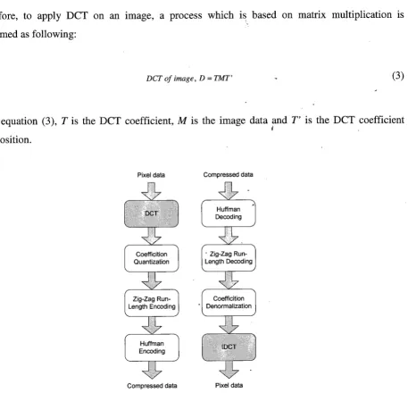
732.6 Application: Discrete Cosine Transform
...
752.7 FPGA Implementation
...
782.7.1 ENSTA APIs
...
782.7.2 Parallel Prograrnmming
...
7 92.8 Results and Discussion
...
80Conclusion
...
833
.
OVERVIEW OF 3D IC TECHNOLOGY...
853.1 2D Architecture and Its Issues
...
853.2 3D IC Technology
...
88...
3.2.1 Advantages of 3D IC Technology 9 1 3.2.2 TSV Technology...
933.2.3 Stacking Techniques for 3D IC Technology Manufacturing
...
95...
3.2.4 Partitioning Granularities for 3D Architecture Implementation 99 3.2.5 Tezzaron 3D IC Technology...
1003.3 CMOS Scaling vs 3D IC Technology
...
:
...
1043.4 Challenges of 3D IC Technology
...
1053.5 3D IC Technology Standards
...
108...
3.6 State of the art of 3D IC Architecture Implementations :...
109...
Conclusion 1 1 5 / 4.
3D DESIGN FLOW FOCUSING ON TIMING VERIFICATION...
1174.1 Related Works on 3D Design Flow
...
117...
4.2 Proposed 3D Design Flow with Timing Verification 1 2 3 4.2.1 3D Physical Design Implementation Flow...
:
...
123...
4.2.2 Front-end Design Flow 1 2 5...
4.2.3 Back-end Design Flow 1 2 7 4.2.4 3D Timing Analysis Design Flow...
129...
4.2.5 Limitation of the Flow 1 3 1...
Conclusion 131 5.
EXPLORATION OF 3D NOC ARCHITECTURES THROUGH PHYSICAL DESIGN IMPLEMENTATION...
133...
5.1 Related Works 1 3 4 5.2 Standard Cell Libraries...
1365.3 Baseline NoC Architecture
... ...
137...
5.3.1 Router and NIU Architecture 1 3 7...
5.3.2 Baseline 3D Mesh NoC :...
1405.4 3D NoC Architectures Exploration
...
1415.4.1 3D NoC Partitioning
...
142...
5.4.2 3DNoC 1 : 3D Stacked Mesh NoC 143
...
5.4.3 3DNoC2: 3D Stacked Hexagonal NoC 1 4 5
5.5 Experimental Results
...
149...
5.5.1 Wirelength Analysis 153
5.5.2 Impact of Wire Delay
...
154...
5.5.3 Extrapolation of Physical Implementation Result 1 5 5
5.5.4 Impact of 3D IC design using 2D EDA Tools
...
1 5 6. . ;
5.6 3D IC Implementation for MPSoC Architectures: Mesh and Butteffly NoC
...
:I57 *-9<
f t. . 158
5.6.1 3DMPSoC1: Mesh Topology
...
+:--C....
5.6.2 3DMPSoC2: Butterfly Topology 1 6 0
...
5.6.3 3D MPSoC Implementations Comparison 1 6 2
...
Conclusion 1 6 3
....
6
.
HETEROGENEOUS STACKING OF 3D NOC-BASED MPSOC ARCHITECTURE 165...
6.1 Introduction 1 6 5
...
6.2 Related Works 166
6.3 Baseline 2D NoC-based MPSoC Architecture
...
168...
6.3.1 Processor Architecture 1 6 8
...
6.3.2 NoC Architecture 1 6 9
...
6.3.3 GALS Implementation 1 6 9
...
6.3.4 Baseline 2D MPSoC Architecture 171
...
6.4 Heterogeneous Stacking of 3D NoC-Based MPSoC Architecture 173
...
6.4.1 Partitioning Technique 1 7 3
6.5 Experimental Results
...
1746.5.1.2D vs 3D Clock Tree Analysis
...
179...
6.5.2 2D vs 3D Critical Path Analysis 1 8 3
6.5.3 Impact of Microbumps Pitch
...
186...
6.5.4 Implications of 3D IC Design using 2D EDA Tools 190
Conclusion
...
1907
.
DESIGN SPACE EXPLORATION OF 2D EDA TOOL IMPACT ON THE 3D MPSOCARCHITECTURE
...
191...
7.1 Introduction 191
...
7.2 Related Works 192
7.3 Exploration Configuration
...
193...
7.3.1 Parameters Exploration 1 9 3
...
7.3.2 Exploration Design How 193
...
7.4 3D MPSoC Architectures for the Exploration 194
...
7.5 Exploration Results 197
7.5.1 Pocessor Timing Slack Analysis
...
1977.5.2 NoC Timing Slack Analysis
...
199...
7.5.3 3D Power Consumption Analysis 2 0 0
...
7.6 Impact of using 2D EDA Tool on the Design of 3~ MPSoCArchitecture 202
...
Conclusion 2 0 2
8
.
CONCLUSION AND FUTURE WORKS...
203...
8.1 Summary of Works 2 0 3
...
8.2 Future Works 2 0 5
REFERENCES
...
... ...
207LIST OF FIGURES
Figure 1 : Number of processing engine and logic memory size trends in electronic systems
...
55Figure 2: 3D integration example showing seven stacks of wafer connecting using Cu TSV [6]
....
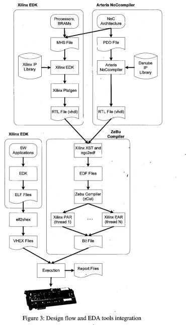
57Figure 3: Design flow and EDA tools integration
...
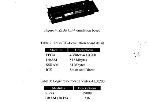
71Figure 4: ZeBu UF-4 emulation board
...
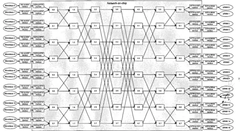
72Figure 5: MPSoC with NoC architecture (a) MicroBlaze core block diagram [3 11 (b) interfa-
ces between components for one MicroBlaze processor (c) complete block diagram ? . o e
. . .
the system
...
...
75 '.P<
4 5 : .
...
Figure 6: 2D NoC-based MPSoC architecture with masters and slaves connection
...
$:.? , 76Figure 7: Example of DCT application in JPEG image compression standard
...
77...
Figure 8: Processor allocation for data parallel of DCT application on 256 x 256 pixels image 79
Figure 9: Execution cycles of MicroBlaze with basic configuration
...
81Figure 10: Execution cycles of MicroBlaze with enhanced configuration
...
82Figure 11: Comparison of execution cycles for MicroBlaze with basic and enhanced configura-
tion
...
82Figure 1'2: Comparison of speedup between MicroBlaze with basic configuration and Micro-
Blaze with enhanced configuration
...
83Figure 13: Evolution of the interconnection architecture for high performance CMOS logic (a)
CMOS 7 s process in 0.2 ym [39] (b) 45 nm process technology [40]
...
86Figure 14: Interconnect and gate delay trends as technology node shrinking
...
87Figure 15: Technology scaling effects on (a) number of repeaters (b) total repeater power [41]
where P is Rent's coefficient
...
87Figure 16: Different type of stacking methods (a) TSV [48] (b) wire bonding [49] (c) contact-
less using inductive coupling [46] (d) contactless using capacitive coupling [45]
...
89Figure 17: Packaging types (a) System-in-Package (Sip) (b) Package-on-Package (POP)
...
89Figure 18: (a) Monolithic 3D IC complete structure (b) transistor level monolithic (c) gate le-
vel monolithic [54]
...
90Figure 19: Reduction of wire length from 2D architecture to 3D architecture with different
...
stacking levels [49] 9 1
Figure 20: TSV manufacturing using (a) laser drilling process and (b) DRIE process [77]
...
94Figure 21: TSV stacking methods (a) via-first and via-last in bulk CMOS (b) via-first TSV in
SO1 CMOS [8 11
...
94Figure 22: 3D stacking methods comparison [82]
...
95...
Figure 23: 3D stacking orientations (a) face-to-face (b) face-to-back (c) back-to-back 96
Figure 24: Examples of 3D stacking orientations (a) face-to-face and face-to-back using MIT
LL technology [84] (b) face-to-face and back-to-back using Tezzaron Technology
[83]
...
96Figure 25: Two-tier Tezzaron 3D face-to-face stacking (a) cross section image of the manufac- tured device (b) cross section of the stacking technology with the corresponding parameters
...
101Figure 26: Tezzaron 3D technology manufacturing process
...
103....
Figure 27: Performance improvement comparison of CMOS migration vs 3D integration [76] 105 Figure 28: Thermal stress from Copper and Tungsen TSV material [I141...
107Figure 29: 3D-MAPS (a) architecture and (b) design summary
...
110Figure 30: 3D NoC (a) architecture and (b) design summary
...
111Figure 3 1: 3D FFT processor layout
...
111Figure 32: 3D SoC (a) architecture (b) 3D stacking diagram (c) design summary
...
112Figure 33: 3D NoC with fault tolerant (a) architecture (b) design summary:
...
112Figure 34: Centip3De (a) architecture and (b) design summary
...
114Figure 35: 3D modular multiprocessor (a) architecture (b) design summary (c) TSV parameters
.
115...
Figure 36: 3D design methodology for timing. power and temperature exploration [13 11 118 Figure 37: 3D ASIC design flow based on standard supkrcell layout [I321...
119Figure 38: CAD flow for via-last face-to-back 3D integration [I331
...
119Figure 39: 3D design flow for three-tier FFT architecture using MIT Lincoln Lab technology [I341
...
120...
Figure 40: Automatic design for 3D microarchitecture performance evaluation [I351 121 Figure 41: Design flow for 3D SAR processor [59]...
122Figure 42: Design flow for 3D hybrid process architecture [S9]
...
123Figure 43: 3D design flow focusing on timing verification
...
124Figure 44: Front-end design flow with timing budgeting flow
...
126...
Figure 45: Back-end design flow with inter-tier signal assignments 128 Figure 46: 3D timing analysis (a) gate-level (b) layout-level with power analysis...
130Figure 47: NIU architecture
...
139Figure 48: 3D Router architecture
...
139...
Figure 49: Packet format of the NoC ;...
140Figure 50: Block diagram of 3D Mesh NoC
...
140...
Figure 5 1 : Floorplan of 3D Mesh NoC 141 Figure 52: Routed layout of 3D Mesh NoC...
141Figure 53: Partitioning method for the 3D NoC architecture (a) baseline 2D Mesh NoC (b)
...
baseline 3D Mesh NoC (c) stacked 3D Mesh NoC 143
Figure 54: Block diagram of 3D Stacked Mesh NoC
...
144Figure 55: Floorplan of 3D Stacked Mesh NoC
...
144...
Figure 56: Routed layout of 3D Stacked Mesh NoC 145
Figure 57: Routing method for hexagonal topology
...
146Figure 58: Block diagram of 3D Stacked Hexagonal NoC
...
148Figure 59: Floorplan of 3D Stacked Hexagonal NoC
...
148Figure 60: Routed layout of 3D Stacked Hexagonal NoC
...
1 9. . .
Figure 61 : Performance comparison of 3D NoC architectures over 2D NoC in 130 nm techno- .. C
4 $7 ,
...
logy 1 5 1
Figure 62: Horizontal wirelength distribution for NoC architectures in 130 nm technology
...
151Figure 63: Performance comparison of 3D NoC architectures over 2D NoC in 45 nm techno-
...
logy 1 5 2
...
Figure 64: Horizontal wirelength distribution for NoC architecture in 45 nm technology 153
...
Figure 65: Tile block floorplan of 3D MPSoC1 (top tier) 159
...
Figure 66: Virtuoso layout of 3D MPSoCl (top tier) 159
...
Figure 67: Tile block floorplan of 3D MPSoCl (bottom tier) 159
...
Figure 68: Virtuoso layout of 3D MPSoCl (bottom tier) 160
...
Figure 69: NoC block diagram for 2D MPSoC2 architecture 161
Figure 70: 3D MPSoC2 block diagram
...
161...
Figure 7 1 : Routed layout of MPSoC2 architecture (bottom tier) 1 6 2
Figure 72: Openfire processor block diagram
...
169Figure 73: Openfire processor internal signals connection
...
170...
Figure 74: Interconnection structure for a complete tile block 170
Figure 75: GALS implementation style using a dual clock FIFO architecture
...
171Figure 76: Baseline 2D MPSoC architecture (a) amoeba view (b) routed layout
...
172Figure 77: Heterogeneous 3D MPSoC stacking
...
173...
Figure 78: Bottom tier of heterogeneous 3D stacking (a) amoeba view (b) routed layout 175
...
Figure 79: Top tier of heterogeneous 3D stacking (a) amoeba view (b) routed layout 176
...
Figure 80: Performance comparison for 2D and heterogeneous 3D MPSoC architecture 178
Figure 8 1: Horizontal wirelength distribution for 2D MPSoC and 3D MPSoC (bottom and top
tier)
...
178Figure 82: Clock tree structure of 2D MPSoC architecture (a) NoC clock (b) processor clock
...
181Figure 83: Clock tree structure for heterogeneous 3D MPSoC stacking (a) processor clock of
...
Figure 84: Critical path for 2D MPSoC (a) processor clock (b) NoC clock
...
184Figure 85: Critical paths of each tier separately in SoC Encounter for the heterogeneous 3D MPSoC (a) processor clock in bottom tier (b) processor clock in top tier (c) NoC clock in top tier
...
186Figure 86: Openfire 3D architecture with 5 pm microbump pitch (a) floorplan of bottom tier with microbumps array on top of memory block (b) routed layout of bottom tier with many DRC violation (c) floorplan of bottom tier with microbumps array on top of processor logic (d) routed layout of bottom tier (e) floorplan of top tier (f) routed layout of top tier
...
188Figure 87: Openfire 3D architecture with 20 I - L ~ microbumps pitch (a) floorplan of top tier (b) routed layout of top tier (c) floorplan of bottom tier (d) routed layout of bottom tier
...
189Figure 88: Design flow for EDA tool exploration
...
195Figure 89: Bottom tier routed layout (top tier has the same layout)
...
196Figure 90: Close-up diagram of tile routed layout
...
196Figure 91: Processor timing slack (WNS) distribution for 3D Mesh MPSoC
...
198Figure 92: Processor Timing slack (WNS) distribution for heterogeneous 3D MPSoC
...
:. ...
198Figure 93: NoC timing slack (WNS) for 3D Mesh MPSoC
...
199Figure 94: NoC timing slack (WNS) for heterogeneous 3D M P S ~ C ~
...
200Figure 95: 3D power consumption for 3D Mesh MPSoC
...
201LIST OF TABLES P
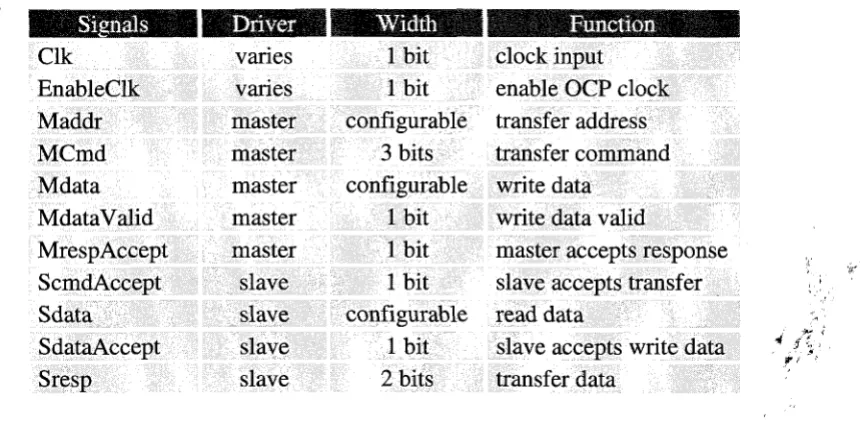
Table 1: OCP-IP interface signals
...
70Table 2: ZeBu UF-4 emulation board detail
...
72Table 3: Logic resources in Virtex 4 LX200
...
72Table 4: ZeBu UF4 operating mode and performance
...
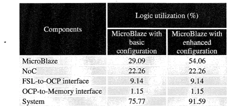
72Table 5: Post place and route logic utilization for MicroBlaze with basic and enhanced configu- ration
...
:.
...
78Table 6: OCP master command signals
...
-....
79+- t f : Table 7: Execution cycles for different number of proce3sors and different MicroBlaze configu-
...
rations 8 1 Table 8: Comparison of wafer bonding technology [92]...
98Table 9: Comparison of stacking granularities for 3D architecture design
...
99Table 10: Electrical and thermal properties of several materials
...
107Table 11: Summary of published 3D standards
...
109Table 12: 3D architecture implementations summary
...
116...
Table 13: Physical design parameters using 130 nm standard library 1 3 6 Table 14: Physical design parameters using 45 nm standard library...
137Table 15: NoC topology comparison
...
147Table 16: Performance comparison of 3D NoC architectures in 130 nrn technology
...
150Table 17: Performance comparison of 3D NoC architectures in 45 nm technology
...
152Table 18: Extrapolation of delay for 3D NoC topologies using different process technologies and network diameter comparison
...
156Table 19: MPSoCl physical design characterics
...
160Table 20: 3D MPSoC implementations comparison
...
162Table 21: Synthesize area for each block in a tile
...
172Table 22: Performance comparison for 2D and 3D heterogeneous stacking
...
177Table 23: Clock tree structure properties for 2D and 3D designs
...
183Table 24: Timing performance of different microbumps pitches (target clock period of 10 ns)
....
189Table 25: EDA tool options for design space exploration
...
193Table 26: Summary of design space exploration
...
194CHAPTER 1
INTRODUCTION
Electronic designs have been growing rapidly for the past several years triggered by the rising
demand of smartphones and tablets in the market. The high-end mobile devices increase the
demand for more functionality as well as computing power to be able to run many more
applications. Small form factor, higher performance and lower power are among the important
requirements for the mobile devices in order to deliver smaller, cheaper and faster consumer
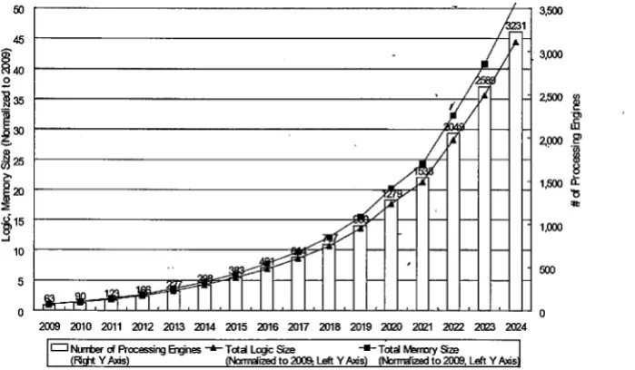
electronic devices. Figure 1 shows the trend for the number of processing elements in SoC
consumer portable devices according to the International Technology Roadmap Semiconductor
(ITRS) [I]. As shown in the figure, in the near future, the number of processing elements is
expected to increase to more than 100 processors. Additionally, the memory size is also projected to
increase dramatically in the future along with the increasing number of processing elements.
0 N m k f d Rasing wries -+ Tdd L q c Size *Tdd f h u r y Sire
[image:16.572.113.463.353.557.2](Rctd Y Ads) (Nolmdized to Left Y Ads) ( N o M d to 2MB. Left Y An's
Figure 1: Number of processing engine and logic memory size trends in electronic systems
Increasing the performance of single processor 'design through higher clock frequency poses
drawback of higher power consumption and thus multiprocessor architecture has been introduced
where a design has several simple processors that run at a lower frequency and lower voltage
supply. Power can be reduced by shutting down idle processors depending on which applications
are running, whle the performance can be improved through parallel execution of applications
using multiple processors. We are moving from computation-extensive architecture to
communication-extensive architecture introduced from this multiprocessor architecture. However,
designing high performance multicore processor architecture requires several challenges to be
CHAPTER 1 Introduction
solved such as interfacing different IP cores, design automation, verification and software
programming [2]. In order to meet the demand of communication requirement, Network on Chip
(NoC) is developed to overcome the limitations of bus based architecture [3]. Some of the
disadvantages of bus architecture are long signal delay due to arbitration policy and complex wiring
that contributes to the overall power consumption of the system. In contrast, NoC offers scalability
and huge amount of communication bandwidth when increasing the number of processors to
perform complex operations [4]. In addition, it supports parallel communication between different
processing elements and also improves communication speed as it does not require &o6al
arbitration policy.
Initially, we rely on the CMOS scaling features to get more performance which is achieved by
reducing the physical dimension of the transistor so that many more transistors can be packed into a
single chip, thus increasing the performance through more deeply pipeline architecture. CMOS
transistor scaling, is a technique to increase the performance of l l k at constant power density by
reducing oxide thickness (t,,), transistor gate length ( I ) , and transistor gate width (w), where k is the
scaling factor. This is true until we reach 130 nm technology because for the following smaller
technology node, enhancers have been added during fabrication processing steps to make sure that
the transistor can be operated at the desired performance. However, moving towards smaller
process technology introduces many great economical and technological challenges and at the same
time decreasing performance benefits at every scaling nodes [5]. For example, in 90 nm and 65 nm
technology, strain has been added, while for 45 nm and 32 nm technology, strain, low-k dielectric
for inter-layer metal insulation and high-k dielectric metal gate have been used to control
transistor's integrity [6] and many more enhancer methods will be needed as we move towards sub-
20 nrn technology. On the other hand, the limitation of CMOS scaling such as maximum voltage
limits and device variability have also impacted design techniques at system and circuit level where
additional design techniques are required to enable increasing performance improvement and power
reduction with cost reduction [7].
Consequently, 3D IC technology enables higher device integration and improves design
performance by stacking wafers or dies on top of the other and interconnected using TSV
technology [8]. It has been studied by several researchers for the past few decades but only now has
gained great attention where it is seen as a promising solution now as many people realize that 2D
scaling is becoming more and more difficult to manufacture. Using this technology, the thin wafers
or dies are stacked in several layers as depicted in Figure 2 as an example and then is packaged
using conventional packaging methodology. This new technology offers potential benefits of faster
Introduction CHAPTER 1
speed, lower power consumption, integration of heterogeneous technology, smaller form factor and
high device integration density. In contrast to CMOS technology scaling, 3D integration is a
promising solution to drive the future of VLSI circuits to support the continuous demand of high
[image:18.561.168.368.153.301.2]performance electronic systems. These benefits will be described in details in the later sections.
Figure 2: 3D integration example showing seven stacks of wafer connecting using Cu TSV [6]
In 3D integration, the long interconnect wire length is reduced to square root of its original length in
2D architecture due to the short vertical connection using- either TSVs or rnicrobumps. This
improves the speed where it reduces the RC delay of the long interconnect wire in 2D architecture
f
and also reduce the number of buffers along the interconnect wire wherein eventually power
consumption is decreased as well. 3D integration also supports integration of heterogeneous
technology such as digital, analog, RF and MEMS technology where they can be fabricated
according to their optimal process technology and then stacked with other process technology.
Finally 3D integration introduces design miniaturization enabling higher density memory or logic
capacity.
Despite the benefits brought by this technology, it also faces several critical obstacles such as
thermal issues, power delivery structure and clock tree synthesis. As 3D integration stacks several
active silicon layers vertically, the device density per unit volume is increased and thereby increases
the power density. Together with the long thermal transfer path between multiple stacked dies and
poor thermal conductivity of dielectric layer in the multiple stacked dies cause the temperature in
the chip to arise. Another effect is that there exist thermal hotspots due to the different power
consumption by different logic blocks in each layer. This generates thermal gradient over the chip
which create variations that could possibly affect the- integrity and reliability of the devices over
time. Power delivery structure also needs to be revised in order to ensure enough current supply to
CHAPTER 1 Introduction
performance out of 3D stacking where TSV plays a crucial role for electrical connections between P
tiers. Although some of the testing techniques for 2D architecture can be extended to enable testing
of 3D architecture such as built-in self test (BIST) and boundary scan method, however the
manufacturing of TSV introduces new defect mechanism such as shorts or opens due to
misalignment and micro-viods and therefore requires a new approach to test these defects. These
are some of the main hurdles in 3D integration technology that need to be solved before it can be
commercially viable in many products.
1.1 Research Motivations
As this is a relatively new technology at the moment, many issues are still being researched
extensively in industry and academics. Looking at the publication in conferences and journals, we
realized that there is a lack of real design and implementation being carried out to have more
realistic results on the performance analysis of this technology. In pacticular, research works in 3D
NoC architecture have been done mostly using software simulation using cycle-accurate simulator
which provide unrealistic results and thus are not sufficient to evaluate the pros and cons of 3D
technology. Therefore, one of the main motivations in this work is to conduct performance analysis
by using real design and implementation of 3D technology using technology that are available to
use. Through this approach, we aim to have more realistic results and thus could help us to better
understand the trade-off offers using this technology.
A part from that, we focus our work on the architectural aspect of this technology as we have
specifically chosen to use Tezzaron two-tier 3D technology for the technological aspect. Current
electronic devices mostly have more than one processing core in order to have more capability to
run various applications with higher performance. This is due to the fact that the performance of a
single prwessor architecture cannot be improved anymore because of the power wall and the
memory wall. Therefore, it is interesting to know how this 3D technology could be used to
overcome the multiprocessor issues that are being faced now to be able to improve its performance.
Several works have been done performing design and implementation on multiprocessor
architecture using 3D technology where a handful number of works showed quite significant
performance improvement using 3D technology when compared to 2D architecture. However, none
of the previous works analyzed the 3D NoC architecture performance base on real design and
implementation results, which is the main objective of this work. It is interesting to understand what
kind of NoC topologies (2D or 3D topologies) is better in 3D architecture in terms of performance
where we do not have to consider it when designing a 2D architecture. On the other hand, research
Introduction CHAPTER 1
works on 3D GALS-based multiprocessor architecture have also not been reported especially
concerning physical design implementation issues. This is the reason that motivates us to design
and implement this type of architecture to be able to conduct performance analysis when compared
to its 2D implementation and identify physical design issues that need to be taken into consideration
during the design process.
A common approach to design 3D architectures is to use-the state of the art 2D EDA tools as has
been reported by many works in the literature since there are no commercial true 3D design tools
available in the market to date. This approach does not guarantee maximum performance gain of the
3D architecture over its 2D architecture because 2D EDA tools are not able to see the complete 3D
architecture to be able to perform necessary optimization processes to achieve the target
performance requirements. The lack of study in the literature regarding what is the impact of 2D
EDA tools on the 3D architecture performance motivates us to conduct a design space exploration
experiment of 3D MPSoC architecture to investigate this issue in details.
1.2 Summary of Arguments
1.2.1 Deep Understanding about the Target Architecture to Maximize Performance
Improvement
In this thesis, although many previous published papers have shown that 3D IC technology gives
many advantages in terms of area, performance and power when implemented using 2D design
tools, we argue that there is still a need for the careful architectural decisions in order not to
diminish the potential benefits it could offer. Bad architectural implementation choices such as bad
partitioning methods (with manual and not optimize' partitioning), bad TSVs/microbumps planning
and bad 3D specific architecture (such as 3D NoC topology vs 2D NoC topology) particularly for
heterogeneous 3D stacking can only make the performance worse than its 2D architecture or if not
worse, will only give marginal improvement to be able to justify the devoted design efforts and time
for designing in 3D technology. Deep understanding about the target architecture to be
implemented as well as the target 3D IC technology to be used are completely essential to help
making the right decision on choosing various 3D specific -parameters such as power delivery
methods, clock tree structure, TSVs count and location, power and thermal management methods
CHAPTER 1 Introduction
1.2.2 Process Technologies for 3D IC Technology Depending on the Different Target
~mplementations
On the other hand, although the current 3D IC technologies that are available today such as
Tezzaron two-tier technology using bulk CMOS 130 nm technology of Global Foundries, lMEC
technology using bulk CMOS 130 nm technology and MIT LL three-tier technology using FDSOI
180 nm technology, we argue that implementing 3D IC technology using advanced process
technology such as 45 nm is more appealing for high performance computing due to the fact that in
advanced technology global delay is heavily dominated by wire delay propagating through high
3Y '
number of metal interconnect layers thereby will have stronger impact on the p&f&mance
improvement of the 2D architecture than in older process technology. Using heterogeneous 3D IC
technology that stacked different architectures that have been optimized in their own matured
process technology is a more attractive solution to get higher performance improvement. However,
using old process technology for 3D architecture implementation can be considered for low-end
devices to improve performance of previously developed 2D devices due to the cost issues when
migrating to the other process technologies.
1.2.3 3D-aware EDA Tools with 3D Optimization Capability for Designing 3D IC Technology
From the design perspective, true 3D aware tools for designing 3D architectures that are capable of
doing 3D aware design and optimization such as 3D synthesis, placement, clock tree synthesis and
routing under various design constraints such as timing, power and thermal constraints are
absoliftely needed to be able to gain the highest possible performance improvement from 3D
technology. Although current matured 2D EDA tools can be used to design 3D architectures with
some design flow modifications customized to the specific 3D IC technology target, we argue that
the performance improvement is still limited to the architectural implementation choices as
mentioned earlier and we do not have full control over architectural parameters of a complete 3D
design to do an architectural analysis before making decisions on the best architecture to be
implemented whereby the 2D tools are not aware of the complete 3D design when optimizing it to
meet the design constraints especially tight design constraints for high performance arhitectures.
Furthermore, designing 3D architecture using 2D tools requires much more efforts whereas if using
true 3D-aware tools, it will be more productive as it allows designers to concentrate more on the 3D
architectural issues for a given particular target device rather than spending time and resources
Introduction
1.3 Thesis Contributions
CHAPTER 1
The contributions of this thesis are summarized as follows:
1. Proposed novel design flow for 3D architecture design using available 2D EDA tools primarily
focusing on 3D timing verification. This 3D timing verification is possible because vertical
inter-tier connection is created using microbumps which has negligible delay in this particular
3D technology. The proposed 3D design method has been used for the experiments in this thesis
conducted to study various architectural implementations that are feasible using 3D technology.
As will be explained in detail in Chapter 2, the proposed methodology offer several advantages
such as early and more accurate 3D performance estimation through post synthesis netlist
timing analysis and allow faster 3D architectural exploration to find an optimized architecture to
obtain the most benefit from stacking dies.
2. Presented NoC architectures exploration in 3D architecture through physical design
implementation motivated from the earlier studies in the literature that carried out performance
analysis from software implementation. We designed and implemented 3D Mesh NoC
architecture and 3D Stacked Mesh NoC architecture using homogenous~stacking of 2D router
architecture in two tiers using Tezzaron 3D technology and compared its performance with the
2D NoC architecture. We proposed a new topology for 3D NoC architecture which is hexagonal
topology that provides better performance than the other architectures in 3D technology
implementation due to the equal inter-router wire length.
3. Conducted heterogeneous 3D stacking implementation for GALS multiprocessor architecture by
stacking NoC architecture on top of the processor due to the limited number of works in 3D
architecture based on GALS implementation. Among the benefits of this stacking method are
better control of thermal and power management methods due to the separate physical layer of
the architecture having different thermal and power consumption profile. In this study, we
analyzed the performance of heterogeneous 3D stacked architecture that have been manually
partitioned into two tiers and compared with its correspondent 2D architecture to identify design
trade-off as well as physical design implementation issues. We also conducted analysis on wire
delay effect to the 3D NoC architectures performance by doing physical design implementation
through two standard cell libraries representing old and ad~anced process technologies.
4. Carried out a design space exploration of 3D MPSoC architecture to analyze the impact of 2D
EDA tools to its performance such as timing quality, power consumption and wirelength. Since
it is understandable the limitation of using 2D EDA tools- to design and implement 3D
architecture, this study investigated the performance impact of 3D MPSoC architecture when
CHAPTER 1 Introduction
2D EDA tool options, in particular the placement and routing options is varied enabling us to
understand several important implementation issues that have not been pointed out previously.
We focus on timing and power optimization options in the 2D EDA tools for the exploration
because both metrics are among the most essential parameters that are considered during the 3D
architecture design.
1.4 Thesis Organization
#'
This thesis is organized as follows: In the next chapter (Chapter 2), we present our initial wprk on '
4 :< ' 2D NoC-based MPSoC design and implementation to identify design issues related to thg;'MPSoC
architecture before embarking on the 3D IC research work.
Chapter 3 briefly explains the overview of 3D IC technology by firstly introducing the issues being
faced by the current 2D architecture. Then we look into different aspects of 3D technology
including TSV structure, bonding methods, stacking orientation and several other challenges that
need to be overcome before this technology can be adopted as a mainstream technology. The 3D
standards are also presented highlighting the need for standards in various aspects of 3D technology
because through standardization it would make adoption of this technology faster. Finally we
present the state of the art 3D architecture implementations that have been completed to date
targeting various design objectives revealing the concrete proof of the benefits of this technology
that have been discussed earlier in the chapter.
Chapter 4 discusses a proposed design methodology specific to the Tezzaron 3D technology two-
tier face-to-face integration but architecturally generic. This design flow takes benefits from the
small structure of microbumps having smalllnegligible delay for the vertical inter-tier connections.
Therefore,-performing 3D timing analysis at post-synthesis stage allows us to verify the 3D design
early in the design stage rather than post-place and route stage. After analyzing the timing path in
the 3D design, necessary modification in the RTL can be done to achieve its target performance
without having to wait until finish place and route the design that save a certain amount of time.
Chapter 5 explains about the exploration of 3D NoC architecture through design and
implementation using Tezzaron two-tier technology. Performance analysis is conducted based on
the routed netlists. Current 2D EDA tools have been used for the implementation based on the
methodology explained in Chapter 4. We compare the 3D NoC architecture implementations in
order to obtain the best topology to be used for the 3D technology. Two standard cells technologies
Introduction CHAPTER 1
have been used for the implementation to have better understanding about the effect of wire delay to
the performance of 3D architectures. We also present our target 3D IC designs being developed to
be sent for fabrication comparing two MPSoC designs developed by two teams, the GIPSA-Lab
team and the ENSTA ParisTech team. The MPSoC architectures used different NoC topologies in
order to measure their performance in real implementation when running applications and also to
study various 3D implementation issues.
Chapter 6 describes the design and implementation of heterogeneous 3D stacking MPSoC
architecture employing GALS style to analyze various architectural trade-off. This chapter features
another feasible 3D NoC-based MPSoC implementation through heterogeneous implementation by
stacking different architectures on different layers using similar process technology. We conduct
several analyses regarding the clock tree structure and critical paths between 2D MPSoC and
heterogeneous 3D MPSoC to highlight design and implementation issues with respect to the use of
2D EDA tools. Additionally, we perform experiment on varying microbumps pitch and location for
the vertical connection and study its implication on the performance of the 3D architecture
identifying the limitations it could impose for designing complex 3D application when using 2D
EDA tools.
I
Chapter 7 presents a design space exploration of 3D MPSoC architecture using 2D EDA tool to
analyze the impact of EDA tool on 3D architecture performance as well as to highlight design
issues related to designing 3D architecture. Since true 3D design tools are not available until now,
specifically design tools that are capable of doing 3D physical, design as well as optimization, this
exploration allows us to have better understanding about how different options in the EDA tools
lead to different optimization results of 3D architecture.
Chapter 8 concludes the works presented in this thesis. It also highlights main contributions
reported in this thesis to obtain more understanding of 3D integration focusing on architectural
point of view. Future works based upon the works conducted in this thesis are also proposed for
CHAPTER 2
2D NOC-BASED MPSOC DESIGN AND IMPLEMENTATION ON FPGA
The era of multiprocessor system-on-chip (MPSoC) has brought a new challenge for modern
electronic systems. Communication between IP cores and other peripheral in the MPSoC
environment is becoming critical which will affect the performance. Network-on-Chip (NoC) is a
promising solution for MPSoC communication limitation. several NoC studies have been reported
over the years but only a few discussed about the actual hardware implementation. In this chapter,
we presented FPGA design and implementation of MPSOC system with NoC architectures in order
to obtain its actual performance. To improve design productivity, we use Arteris design tool to
automatically generate NoC architectures and also supports various interface protocols to other IPS.
A case study of Discrete Cosine Transform (DCT) using parallel programming is carried out to
validate the design. The goal of this chapter is to present our initial work regarding the 2D NoC-
based MPSoC implementation on FPGA which enable us to identify design issues for NoC
implementation before proceeding with the 3D IC design process.
2.1 Introduction
I
MPSoC has been emerged over many years in response to the need of embedded computing
requirements such as handheld devices and laptop computers. This is in contrast to the multicore
processors that do not have tight requirement commonly use in desktop computer and server
applications. The need for programmability, high performance in real time application and low
power operation are among the main motivation of MPSoC for various embedded system
applications which includes multimedia, signal processing and automotive [9]. As embedded
systems demand high performance to support multiple functions, large scale MPSoC design has
been emerging. With the current IC technology allows us to use million of transistors in a chip,
large scale MPSoC is possible. However, the performance of large scale MPSoC may be degraded
due to the communication efficiency between processors and other IPS.
Traditional bus based architecture and dedicated interconnection managing communication in the
MPSoC system face several drawbacks such as less scalable, complex wiring connection which
contribute to large power consumption, low performance due to arbitration scheme and less design '
space exploration. Shared bus interconnection has limitation in its scalability because all bus
accesses must be serialized by the arbitrator. Bus structure cannot handle in environment such as
CHAPTER 2 2D NoC-Based MPSoC Design and Implementation on FPGA
on large wiring delay when large number of components attached to the bus due to the physical
capacitance of the bus wires grows. Shared bus offers system reusability and available bandwidth is
shared among nodes but reduce operating frequency with system growth. Advantage of bus
architecture is enhanced communication performance but poor reusability where dedicated channel
cannot scale well with system complexity [lo]. Advance bus architectures are also were proposed
such as ARM AMBA [ l l ] , OpenCore WISHBONE system on chip interconnection [12], ST
Microelectronic Bus (STBus) [13] and IBM Coreconnect [14] as the extended version to achieved
high performance of bus architecture. Advanced bus architecture adopt hierarchical structure in
order to get scalable communication throughput and partition communication domains into skeral 4 < Y i
group of communication layers depending on the bandwidth requirement such as performan$$.;
Networks-on-chip (NoC) provides solution to the limitation of bus based architecture and'dedicated
interconnection scheme in multiprocessor system-on-chip (MPSoC) design. NoC architecture offers
scalability and flexibility of MPSoC design to achieve better performance as well as supporting
large scale MPSoC design. By facilitating NoC in the MPSoC system, adding additional elements
in the system is not requiring too much effort. It is also can be used to integrate different type of
components as the NoC architecture is only dependant on the protocol for its interface. Due to less
complex wiring, NoC improve the MPSoC design by using less hardware area, better performance,
and also less power consumption because of shorter wiring distance between components [15].
Network on chip provide scalability and freedom from the limitation of complex wiring. Using
NoC, wiring for the interconnection is shorten. NoC reduce SoC manufacturing cost, SoC time to
market, SoC time to volume, increase SoC performance. NoC also increase system throughput.
NoC offers high flexibility and regularity of a network structure supporting simpler interconnect
models and greater fault tolerance. NoC able to integrate many different IP cores such as
processors, DSP cores, memory blocks, FPGA blocks, dedicated hardware. NoC provide good
solutions in-numerous applications [16] such as flexible product that should be reconfigurable and
programmable, applications with heterogeneous task mix, design which are basis of several product
variants, applications with stringent time-to-market requirements, products where reuse at the
block, function and feature level is considered valuable.
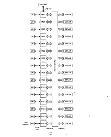
In this work, we demonstrated MPSoC design with 16 MicroBlazes as masters and 16 BRAMs as
slaves. The masters and slaves are connected through 2-ary 4-tree NoC architecture. Several
interfaces have been designed to accommodate different communication standard between
MicroBlaze and BRAM with the NoC. Additional Application Programming Interface (APIs) is
also developed used for synchronization of the masters. For the evaluation methodology, parallel
2D MPSoC Design and Implementation on FPGA CHAPTER 2
programming for Discrete Cosine Transform (DCT) application is tested on the design based on
several image size and different MicroBlaze configuration.
2.2 Related Works
Mesh and Torus topology have been the popular choice for FPGA implementation because of it's
simple routing algorithm and easy implementation on hardware. Various configuration of master
and slave combination has also been considered in previous work. In [17], FPGA implementation of
Torus topology is presented and proposed new router architecture and algorithm to solve congestion
problem from Mesh topology. Design and implementation on Altera Stratix II FPGA for 2D Mesh
architecture is presented by [18] with the aim to evaluate scalability of Mesh network by
experimenting different number of processing elements. Another 2D Mesh architecture prototyping
in FPGA is reported in [19] where they evaluate Mesh NoC to compare with shared-bus and point-
to-point architecture. In [20], 3 x 3 Mesh network was designed and implemented and has been
tested for Charge-Coupled Device (CCD) application. They designed custom router architecture
based on circuit switch protocol. Other than regular NoC topologies, work on custom NoC
topologies have also been developed such as SUNFLOOR [21] and SPIN [22]. Work on parallel
implementation for DCT has also been presented in the literature: Jn [23], MPSoC design using
custom system level design framework called Deadalus was presented by implementing JPEG-
based image compression to Xilinx FPGA. Different number of MicroBlaze processors as well as
dedicated DCT cores, which is up to 16 MicroBlazes and 8 DCT IPS were designed with exploiting
task and data parallelism for the target JPEG application. Th? speed up of almost 20 times is
achieved using combination of MicroBlaze processors and DCT cores. Homogeneous MPSoC
system for JPEG application also has been reported in [24] implemented on Xilinx V4 LX25
FPGA. The MPSoC comprises up to four MicroBlazes which achieved the speed up of three times.
Another work proposed parallel implementation of DCT on two DSP processors which shown
increasing speed up calculation time [25]. This work proposed MPSoC based on 16 MicroBlazes
implemented on Xilinx V4 LX200 FPGA. Several EDA tools have been used throughout the design
to improve design productivity for designing large and complex system. Furthermore, NoC
architecture is used for communication within the MPSoC system.
2.3 EDA Tools Integration
EDA tools play an important role in the development of electronic design to achieve various
CHAPTER 2 2D NoC-Based MPSoC Design and Implementation on FPGA
use several EDA tools to complete the design and execution of FPGA which are Arteris
~ o ~ c o m ~ i l e r version 1.12 from Arteris [26], Xilinx ISE and EDK 9.1 from Xilinx [27], and ZeBu
Compiler from EVE [28].
NoCcompiler is a NoC configuration environment for Arteris NoC
IP
Library. Arteris NoCTransport and Transaction Protocol (NTTP) is packet-based NoC architecture. In order to provide
communication between IP blocks over a NoC, the NTTP uses three layer approaches which are
transaction, transport and physical layers. Transaction layer has Network Interface Units (NILk)
such as AMBA High Performance Bus (AHB), AMBA Advanced Extensible Interface (AXI) and 4 <%
Open Core Protocol (OCP) that define exchange of information between NIU to perfon$ kertain
transaction. For OCP interface, the NIUs are compliant with OCP 2.2. Each master (or initiator) and
slave (or target) are connected to a NoC using OCP-to-NTTP and NTTP-TO-OCP NIUs
respectively through a socket. OCP-to-NTTP NIUs allow master to be connected to the NoC by
translating OCP transactions into equivalent NTTP packet sequence and vice versa NTTP-to-OCP
NIUs. It supports OCP data bus of 32, 64 and 128 bits which is manually specifies by designer.
Transaction between NIU and IP blocks can be of request or response. Most transactions are in two
steps; a master sends request packets and a slave response packets. In the transport layer, the
packets are routed through the NoC using Packet Transport Units (PTUs) such as switches,
adapters, converters and others. Request packets can be 33 or 36 bits for data cell while for response
packets the data cell size is always 33 bits.
Next, physical connection of the packet in the NoC is defined in the physical layer. Switch is an
essential element of the NoC. It receives packets from input ports and forwards each packet to a
specific output port. In this work, the switch is based on the Arteris Danube IP Library. It uses
wormhole routing algorithm to reduce latency and has full throughout arbitration due to one routing
decision peg input per cycle. NoC architecture from NoCcompiler can be exported to synthesizable
RTL files either in VHDL, SystemC or Verilog. The same flow has been used previously in
different works [29]. Xilinx Embedded Development Kits (EDK) is a set of tools and Intellectual
Property (IP) for developing embedded processor system targeting Xilinx FPGA devices. EDK
provide an environment for designing complex embedded systems combining hardware blocks and
software applications. Processors and other peripherals are connected using On-Chip Peripheral
(OPB) or Processor Local Bus (PLB). Within the EDK environment, as there is no OCP protocol
support by this tool, two IPS have been developed to interface NoC architecture with Microblaze
processor and BRAM. For the MicroBlaze processor, it used FSL interface because it is simple to
modify in order to design interface to the OCP protocol. The EDK tool is used to build complete
![Figure 2: 3D integration example showing seven stacks of wafer connecting using Cu TSV [6]](https://thumb-us.123doks.com/thumbv2/123dok_us/8773096.899930/18.561.168.368.153.301/figure-integration-example-showing-seven-stacks-wafer-connecting.webp)