N A N O E X P R E S S
Open Access
Effect of mold treatment by solvent on PDMS
molding into nanoholes
Celal Con
1,2and Bo Cui
1,2*Abstract
Polydimethylsiloxane (PDMS) is the most popular and versatile material for soft lithography due to its flexibility and easy fabrication by molding process. However, for nanoscale patterns, it is challenging to fill uncured PDMS into the holes or trenches on the master mold that is coated with a silane anti-adhesion layer needed for clean demolding. PDMS filling was previously found to be facilitated by diluting it with toluene or hexane, which was attributed to the great reduction of viscosity for diluted PDMS. Here, we suggest that the reason behind the improved filling for diluted PDMS is that the diluent solvent increasesin situthe surface energy of the silane-treated mold and thus the wetting of PDMS to the mold surface. We treated the master mold surface (that was already coated with a silane anti-adhesion monolayer) with toluene or hexane, and found that the filling by undiluted PMDS into the nanoscale holes on the master mold was improved despite the high viscosity of the undiluted PDMS. A simple estimation based on capillary filing into a channel also gives a filling time on the millisecond scale, which implies that the viscosity of PMDS should not be the limiting factor. We achieved a hole filling down to sub-200-nm diameter that is smaller than those of the previous studies using regular Sylgard PDMS (not hard PDMS, Dow Corning Corporation, Midland, MI, USA). However, we are not able to explain using a simple argument based on wetting property why smaller, e.g., sub-100-nm holes, cannot be filled, for which we suggested a few possible factors for its explanation.
Keywords:Nanoimprint lithography; Molding; PDMS; Capillary filling; Surface energy
Background
Nanoimprint lithography (NIL), which is not limited by light diffraction as in photolithography or charged beam scattering as in electron/ion beam lithography, is a low-cost and high-throughput process that offers ultrahigh resolution. The mold (or stamp) is typically fabricated from silicon for thermal NIL and quartz for UV-curing NIL, which are rigid and susceptible to breakage that re-duces the lifetime of the mold and increases the cost of the process. A natural solution to this issue is a polymer mold material. Unfortunately, most common polymer materials (polymethyl methacrylate (PMMA), polystyr-ene, polycarbonate, etc.) are not suitable because they are incompatible with anti-adhesion surface treatment needed for clean demolding. The mold material has to either possess a low surface energy such as those
containing fluorine or contain silicon whose surface can be converted into SiO2 upon oxygen plasma treatment (SiO2 is suitable for anti-adhesion surface treatment). The former group includes perfluoropolyethers [1] and Teflon AF 2400 (DuPont, Wilmington, DE, USA) [2], whereas the latter includes polydimethylsiloxane (PDMS) [3] and Si-containing UV-curable resist [4,5]. Another equally important property of the above mate-rials is that the polymer mold can all be duplicated read-ily from a master mold as they are liquids in the uncured form.
Among the mold materials mentioned above, PDMS is the most popular and versatile mold material for nanoimprint and soft lithography because of its flexibil-ity for conformal contact with non-planar surfaces, high UV transparency, low surface energy, high gas perme-ability, chemical inertness, and ease of handling. How-ever, besides its low Young's modulus, it is found challenging to fill uncured PDMS into the nanoscale pat-tern on the master mold that is coated with an anti-* Correspondence:[email protected]
1Department of Electrical and Computer Engineering, University of Waterloo,
200 University Ave. West, Waterloo, ON N2L 3G1, Canada
2Waterloo Institute for Nanotechnology (WIN), University of Waterloo, 200
University Ave. West, Waterloo, ON N2L 3G1, Canada
adhesion monolayer needed for clean demolding. Previ-ous studies have shown that PDMS filling into a nano-scale pattern can be facilitated by diluting it with toluene or hexane, which was attributed to the great reduction of viscosity for diluted PDMS [4,5]. However, if viscosity is the limiting factor, the hole filling depth should be in-creased with the filling time, which is not the case according to our experiment.
In addition, many reports including the above two are for PDMS filling into protruded features (e.g., an array of pillar) in the master mold that is easier when the pil-lars are well separated than filling into (recessed) holes. This is because for the application as nanoimprint mold, the hole pattern in PDMS (pillar in the master mold) is much more mechanically stable than the pillar pattern (hole in the master mold). For hole filling by PDMS, one study claimed filling of 100- to 200-nm diameter holes in porous alumina, but unfortunately, this claim was not supported by its experimental results [6]. Two other studies on PDMS filling into porous alumina also obtained very shallow and incomplete filling [7,8]. An-other recent study showed complete filling into large 750-nm diameter holes in the silicon master mold coated with anti-adhesion layer [9]. In this study, we achieved a hole filling down to sub-200-nm diameter by additional solvent treatment of the mold that was already coated with an anti-adhesion monolayer. Our study suggests that the wetting properties between PDMS and mold are important for PDMS filling into the nanoscale pattern, and the improved filling by the di-luted PDMS could be mainly due to the diluent toluene or hexane increasing in situ the surface energy of the anti-adhesion-treated mold, rather than due to the re-duced viscosity of the diluted PDMS. As such, our study represents a significant step forward in understanding this very widely employed process. However, even taking into consideration of both viscosity and surface energy/ wetting property, we are not able to explain why smaller holes cannot be filled. Further theoretical and experi-mental study is needed in order to elucidate the hole fill-ing process by PDMS.
Methods
Our silicon master mold contains arrays of nanoholes with diameters ranging from 1,000 nm down to 100 nm and depth close to 1,000 nm, and was fabricated by elec-tron beam lithography and pattern transfer process. The hole array pattern was first exposed in ZEP-520A (Zeon Corporation, Tokyo, Japan) electron beam resist at 20 keV using Raith 150TWO electron beam lithography system (Ronkonkoma, NY, USA). After development using pentyl acetate (Sigma-Aldrich, St. Louis, MO, USA) for 1 min at room temperature, the pattern was transferred into the Al hard mask layer using RIE with
BCl3gas. Next, the pattern was further transferred into the silicon wafer with Al as mask using Oxford Instruments ICP380 dry etching system (Abingdon, UK) with C4F8 and SF6 gases [10], followed by Al removal process. To facilitate demolding of the cured PDMS from the master mold without pattern fracturing, the surface of the silicon master mold was coated with a
self-assembled monolayer of trichloro
(1H,1H,2H,2H-perfluorooctyl)silane (FOTS, Sigma-Aldrich, St. Louis, MO, USA) in a vacuum chamber for 12 h at room temperature. The silane-treated mold was baked at 150° C for 20 min to further lower its surface energy [11].
For the molding process, PDMS (Sylgard 184, Dow Corning, Midland, MI, USA) was first mixed with its curing agent at the ratio of 10:1 and then casted onto the master mold. Next, we left the samples in a vacuum for approximately 2 h for degassing, during which time period the PDMS began to fill the holes on the master mold. Finally, the PDMS was cured at 100°C for 4 h on a hotplate in atmospheric condition and peeled off from the master mold. To study the effect of the additional solvent treatment of the silane-coated master mold on PDMS molding, right before (undiluted) PDMS casting, some master molds were dipped into toluene or hexane for 1 min and dried with nitrogen gun.
Results
Effect of solvent treatment on PDMS filling into nanoholes
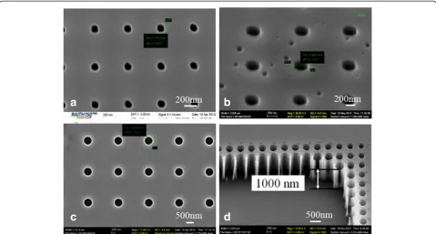
Figure 1 shows the scanning electron microscopy (SEM) image of the master mold consisting of array of holes with various diameters. There are a total of ten different diameters in the mold; shown here are representative three with diameters of 500, 300, and 120 nm (smallest). Figure 1d is the cross-sectional view of the holes with diameter of 300 nm near a large etched area in order to reveal the etched profile, which shows a nearly vertical profile with depth close to 1,000 nm. However, the hole could be slightly shallower for smaller diameters due to the difficulty for etching species to diffuse into and for etching products to get out of the holes. Smaller holes are not necessary for the current study since, anyway, they could not be filled by the PDMS.
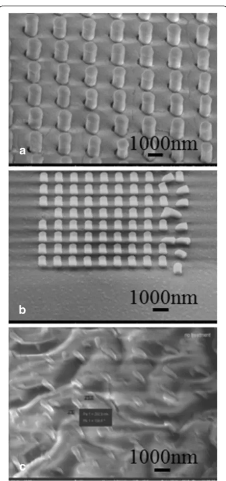
Figure 2 shows the filling of PDMS into the master mold treated with FOTS, but without any additional solvent treatment. For large diameters, the PDMS pillar array has a cylindrical shape matching the hole profile in the master mold. The smallest diameter that PDMS can successfully fill is about 300 nm, though for this diam-eter the pillars were deformed due to PDMS's low Young's modulus and the stress generated during demolding. Smaller holes were not fully filled with the PDMS, having a very short hemi-spherical‘bump’shape rather than a long cylindrical shape.
Con and CuiNanoscale Research Letters2013,8:394 Page 2 of 6
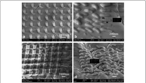
Figure 3 shows the PDMS pillar arrays molded into the master template treated with FOTS, with additional surface treatment using toluene or hexane solvent. The smallest PDMS pillar diameters are 150 and 180 nm for surface treated with toluene and hexane, respectively, which are both smaller than the diameter of the PDMS pillars (300-nm diameter) molded into a master template without solvent treatment. Though the improvement is not dramatic, this indicates that additional solvent sur-face treatment facilitated PDMS filling into FOTS anti-adhesion-treated master mold. It is possible that even though PDMS completely filled into the holes, we did not see PDMS pillars because they were broken during demolding. To verify this, we took SEM images of the master mold after PDMS filling and demolding, which revealed no PDMS left behind on the master mold.
Discussion
In order to explain the enhanced PDMS filling by solv-ent surface treatmsolv-ent, we conducted water contact angle measurement on the three surfaces: FOTS-treated sili-con, toluene- and FOTS-treated silisili-con, and hexane-and FOTS-treated silicon. The average measured contact angles are 107.8°, 104.1°, and 105.9° for the three sur-faces, respectively. Though water contact angle is expected to differ greatly from PDMS contact angle as the two materials are very different, our measurement indicates an increase of surface energy upon additional
solvent treatment, which could lead to an increase or even change of sign of capillary force that is proportional to γsa−γsl (here, γsa is the surface energy of the mold, and γslis the interface energy of PDMS and the mold). This surface energy increase can be explained by the fact that significant percentage of FOTS is actually physically adsorbed (rather than chemically bonded) onto the mold surface and can thus be dissolved by the solvent, which results in the exposure of underneath bare silicon. More complete coverage by chemically bonded FOTS can be obtained through multi-cycle treatment, with each cycle consisting of FOTS treatment followed by dissolving physisorbed molecules.
[image:3.595.58.538.89.346.2]Yang et al. has reported that water filling speed into a parylene microscale channel was increased by 2 orders by pretreating the channel with water, which was attrib-uted to the water molecules' adsorption inside the chan-nel and the resulted modification of parylene's surface energy [12]. As aforementioned, the PDMS filling into the silicon mold structures was improved by diluting it with a solvent such as toluene or hexane, which was at-tributed to the decrease of its viscosity [4]. Indeed, it is known that diluting PDMS drastically reduces its viscos-ity. For instance, its viscosity is reduced to 0.020 Pa · s by diluting it with heptane at 1:2 (PDMS/heptane) ratio [13], and for PDMS oligomers, the viscosity decreased from 0.362 to 0.050 Pa · s when diluted with toluene at 69% by weight [14]. It is fair to estimate that Sylgard 184
PDMS's viscosity is decreased by 1 order if diluted with toluene at 40 wt% (60% toluene, as is the case for [4]). Our study using undiluted PDMS with high viscosity suggests that the improved filling by dilution might be mainly due to the in situ modification of the mold sur-face energy and wetting property by the diluent.
The liquid filling speed into a cylindrical hole can be estimated following the derivation for rectangular holes in [12], as below.
The capillary force applied on the fluid column:Fs= 2πRγlacosθc
The pulling pressure:P¼2πRγlacosθc
πR2 ¼
2γlacosθc
R The gradient of the pressure:−dP
dZ¼Pz¼
2γlacosθc
Rz The velocity profile in a cylindrical hole:
u rð Þ ¼;t 2Vavg 1−r 2
R2
The average velocity:
Vavg¼dzdt¼−R
2
8μ dPdz ¼R
2
8μ2γlaRzcosθc¼ Rγlacosθc
4μz Solving the differential equation:
z¼
ffiffiffiffiffiffiffiffiffiffiffiffiffiffi Rγlacosθc
2μ
q
t;ort¼Rγ2μz2 lacosθc
Here, μ is the dynamic viscosity (3.9 Pa · s for Sylgard
184 PDMS), z is the filling depth (approximately
1,000 nm), γla is the PDMS surface tension, and θc is the contact angle (assume γla× cosθc approximately 0.001 N/m that is a very low value), andRis hole radius (approximately 100 nm), which leads to a filling time of only 0.078 s. The viscosity of the undiluted PDMS is roughly in the same order as that of the PMMA atTg+ 100°C (Tg is glass transition temperature) and is expected to be far lower than that of the polystyrene at 130°C (Tg+ 25°C) due to the exponential relationship be-tween viscosity and temperature, but the latter showed filling of 5-μm deep holes in porous alumina with diam-eter approximately 200 nm within 2 h [15]. Therefore, the poor filling of PDMS into the mold structure cannot be simply attributed to its low viscosity, and surface/ interface property should play an equally important role as discussed above, as well as suggested by the previous study [14].
However, we are unable to explain why smaller holes such as 100- or 50-nm diameter were not filled with PDMS. In principle, as long as the PDMS‘wets’the mold, the filling time (∝1/R) should not increase drastically for smaller hole sizes (actually, in our experiment, the smaller holes could not be filled by increasing the filling time). Therefore, PDMS filling and curing into the nano-scale structures cannot be explained by the classical ca-pillary liquid filling process, and other factors have to be taken into consideration, such as the following:
[image:4.595.58.289.84.575.2]1) PDMS curing: volume shrinkage and curing time. The volume shrinkage of approximately 10% upon PDMS curing may pull out the PDMS structure that was already filled into the holes. For diluted PDMS, significant volume shrinkage occurs when solvent is evaporated, which may also pull out the filled PDMS. As for the curing time, to a certain extent, longer curing time is desirable since the filling will
Figure 2SEM images of PDMS pillars.The pillars were fabricated by molding with undiluted PDMS into the FOTS-treated master mold without additional solvent treatment. The pillar diameters are (a)760 nm,(b)500 nm,(c)300 nm. Smaller holes were not filled. Pillar deformation and significant charging during SEM imaging are evident in(c). Samples were tilted 45° for SEM imaging.
Con and CuiNanoscale Research Letters2013,8:394 Page 4 of 6
stop once PDMS was cured/hardened. The curing can be delayed by diluting PDMS with a solvent. In one study, a‘modulator’that lowers the cross-linking rate was introduced to PDMS and resulted in improved filling into 1D trenches [15]. However, the trench in that study is very shallow; thus, if PDMS can wet and fill the trench, it should fill it
instantaneously. Therefore, the delay of curing might only help assure complete solvent evaporation before hardening.
2) The fact that the holes in our experiment are not open ended, and the trapped air could be compressed when the hole is being filled with PDMS from the top, which would in turn push the PDMS back. However, this factor should be insignificant as it was found that for smaller holes, the PDMS formed only very shallow bumps, so it did not fill the hole and thus the trapped air was not compressed. Moreover, the vacuum level (between 0.01 MPa and 10 Pa) was found unimportant for PDMS filling, though it affected the mechanical properties of the filled PDMS since the PDMS cured at poor vacuum was less dense due to trapped air and solvent molecule [16]. That is, the air at the dead end would dissolve in PDMS rather than get compressed since PDMS is air permeable.
3) Composition of the Sylgard 184 and its curing agent, which contains many additives. One important additive is silica nanoparticle filler for reinforcing purpose [17,18], which may block the hole when its size is not negligible compared to the hole diameter. 4) Size effect. The above derivation for capillary filling
speed applies to large channels. For nanoscale holes, the filling mechanism is much more complicated. For example, the surface energy can differ significantly from macro-scale surface when the liquid pillar diameter is no longer orders larger than the range of van de Waals force, and the meniscus may be‘pinned’due to the abrupt change of surface topography or charges. In addition, at nanoscale, highly viscous fluid usually behaves like non-Newtonian fluid with much higher effective viscosity. Molecular dynamic simulation can be employed to better understand the PDMS filling mechanism.
[image:5.595.56.540.89.363.2]Our current study only serves to suggest alternative roles of solvent in PDMS filling, and it cannot identify which factors play the most critical role in filling nano-scale holes. Systematic further study is needed to unam-biguously elucidate the role of solvent for the hole filling by diluted PDMS, and why sub-100-nm holes are so dif-ficult to fill. For instance, in order to focus on the effect
of viscosity, pure PDMS with different molecular weights, thus very different viscosities, must be used to fill open-ended holes and examined in its liquid state (without curing). This will be studied and published else-where. From the point of view of practical application, PDMS filling into nanoscale holes can be improved by solvent dilution, surface treatment by solvent or surfac-tant other than FOTS such that the surface energy is just low enough for clean demolding, vacuum to drive off solvent and assure PDMS's mechanical property, and applied pressure that is the most effective approach [4].
Conclusions
We, here, studied the effect of solvent treatment of the master mold surface (that was already coated with a si-lane anti-adhesion monolayer) on PDMS filling into nanoscale holes on the master mold. We achieved im-proved filling into holes with diameter down to sub-200 nm versus approximately 300 nm for master mold with-out this additional solvent surface treatment using tolu-ene or hexane. Thus, we suggest that the improved filling by PDMS diluted with the same solvents is due to thein situsurface energy and wetting property modifica-tion by the solvent diluents, rather than due to the greatly reduced viscosity as proposed by previous stud-ies. However, we are not able to explain why smaller holes (e.g., sub-100-nm diameter) cannot be filled, for which we suggested a few possible factors for its explanation.
Competing interests
Both authors declare that they have no competing interests.
Authors’contributions
CC carried out the experiments and drafted the manuscript. BC guided the study and revised the manuscript. Both authors read and approved the final manuscript.
Authors’information
CC received his masters degree from the University of Waterloo in 2011 and is now continuing his PhD study at the same institute. BC is an Assistant Professor at the Department of Electrical and Computer Engineering, University of Waterloo.
Acknowledgements
The authors want to thank Hamed Shahsavan for his help with contact angle measurement, Xiaogan Liang from the University of Michigan, and Tom Glawdel from the University of Waterloo for their helpful discussions. CC acknowledges The Ministry of Turkish National Education for financially supporting his study. This work was carried out using the nanofabrication facility at Quantum NanoFab funded by the Canada Foundation for Innovation, the Ontario Ministry of Research & Innovation, and Ministry of Industry, Canada.
Received: 31 July 2013 Accepted: 5 September 2013 Published: 23 September 2013
References
1. Con C, Zhang J, Jahed Z, Tsui TT, Yavuz M, Cui B:Thermal nanoimprint lithography using fluoropolymer mold.Microelectron Eng2012,
98:246–249.
2. Khang DY, Lee HH:Sub-100 nm patterning with an amorphous fluoropolymer mold.Langmuir2004,20:2445.
3. Cattoni A, Chen J, Decanini D, Shi J, Haghiri-Gosnet A-M:Soft UV nanoimprint lithography: a versatile tool for nanostructuration at the 20nm scale. InRecent Advances in Nanofabrication Techniques and Applications.Edited by Cui B. Rijeka, Croatia: Intech; 2011:139–156. 4. Koo N, Bender M, Plachetka U, Fuchs A, Wahlbrink T, Bolten J, Kurz H:
Improved mold fabrication for the definition of high quality nanopatterns by soft UV-nanoimprint lithography using diluted PDMS material.Microelectron Eng2007,84:904.
5. Koo N, Plachetka U, Otto M, Bolten J, Jeong J, Lee E, Kurz H:The fabrication of a flexible mold for high resolution soft ultraviolet nanoimprint lithography.Nanotechnol2008,19:225304.
6. Ting Y, Shy S:Fabrication nano-pillars pattern on PDMS using anodic aluminum oxide film as template.Proc of SPIE2012,8323:83232H. 7. Zhou W, Zhang J, Li X, Liu Y, Min G, Song Z, Zhang J:Replication of mold
for UV-nanoimprint lithography using AAO membrane.Appl Surf Sci2009,
255:8019.
8. Zhou W, Niu X, Min G, Song Z, Zhang J, Liu Y, Li X, Zhang J, Feng S:Porous alumina nano-membranes: soft replica molding for large area UV-nanoimprint lithography.Microelectron Eng2009,86:2375. 9. Byun I, Park J, Kim J, Kim B:Fabrication of PDMS nano-stamp by
replicating Si nano-moulds fabricated by interference lithography.Key Eng Mat2012,516:25–29.
10. Khorasaninejad M, Walia J, Saini S:Enhanced first-order Raman scattering from arrays of vertical silicon nanowires.Nanotechnol2012,23:275706. 11. Chen JK, Ko FH, Hsieh KF, Chou CT, Chang FC:Effect of fluoroalkyl
substituents on the reactions of alkylchlorosilanes with mold surfaces for nanoimprint lithography.J Vac Sci Technol B2004,22:3233.
12. Yang LJ, Yao TJ, Tai YC:The marching velocity of the capillary meniscus in a micro channel.J Micromech Microeng2004,14:220.
13. Abdelgawad M, Wu C, Chien W, Geddie WR, Jewett MAS, Sun Y:A fast and simple method to fabricate circular micro channels in
polydimethylsiloxane (PDMS).Lab Chip2011,11:545.
14. Kang H, Lee J, Park J, Lee HH:An improved method of preparing composite poly (dimethylsiloxane) mould.Nanotechnol2006,17:197. 15. Zhang M, Dobriyal P, Chen J, Russell TP:Wetting transition in cylindrical
alumina nanopores with polymer melts.Nano Lett2006,6:1075. 16. Ye X, Liu H, Ding Y, Li H, Lu B:Research on the cast molding process for
high quality PDMS molds.Microelectron Eng2009,86:310.
17. Olah A, Hillborg H, Vancso GJ:Hydrophobic recovery of UV/ozone treated poly (dimethylsiloxane): adhesion studies by contact mechanics and mechanism of surface modification.Appl Surf Sci2005,239:410–423. 18. Efimenko K, Wallace WE, Genzer J:Surface modification of sylgard-184
poly (dimethyl siloxane) networks by ultraviolet and ultraviolet/ozone treatment.J Coll Interf Sci2002,254:306–315.
doi:10.1186/1556-276X-8-394
Cite this article as:Con and Cui:Effect of mold treatment by solvent on PDMS molding into nanoholes.Nanoscale Research Letters20138:394.
Submit your manuscript to a
journal and benefi t from:
7Convenient online submission
7Rigorous peer review
7Immediate publication on acceptance
7Open access: articles freely available online
7High visibility within the fi eld
7Retaining the copyright to your article
Submit your next manuscript at 7 springeropen.com
Con and CuiNanoscale Research Letters2013,8:394 Page 6 of 6