N A N O E X P R E S S
Open Access
Ag
2
S/CdS/TiO
2
Nanotube Array Films with
High Photocurrent Density by Spotting
Sample Method
Hong Sun, Peini Zhao, Fanjun Zhang, Yuliang Liu and Jingcheng Hao
*Abstract
Ag2S/CdS/TiO2hybrid nanotube array films (Ag2S/CdS/TNTs) were prepared by selectively depositing a narrow-gap semiconductor—Ag2S (0.9 eV) quantum dots (QDs)—in the local domain of the CdS/TiO2nanotube array films by spotting sample method (SSM). The improvement of sunlight absorption ability and photocurrent density of titanium dioxide (TiO2) nanotube array films (TNTs) which were obtained by anodic oxidation method was realized because of modifying semiconductor QDs. The CdS/TNTs, Ag2S/TNTs, and Ag2S/CdS/TNTs fabricated by uniformly depositing the QDs into the TNTs via the successive ionic layer adsorption and reaction (SILAR) method were synthesized, respectively. The X-ray powder diffraction (XRD), scanning electron microscopy (SEM), transmission electron microscopy (TEM), and X-ray photoelectron spectrum (XPS) results demonstrated that the Ag2S/CdS/TNTs prepared by SSM and other films were successfully prepared. In comparison with the four films of TNTs, CdS/TNTs, Ag2S/TNTs, and Ag2S/CdS/TNTs by SILAR, the Ag2S/CdS/TNTs prepared by SSM showed much better absorption capability and the highest photocurrent density in UV-vis range (320~800 nm). The cycles of local deposition have great influence on their photoelectric properties. The photocurrent density of Ag2S/CdS/TNTs by SSM with optimum deposition cycles of 6 was about 37 times that of TNTs without modification, demonstrating their great prospective applications in solar energy utilization fields.
Keywords:Nanotube array films; Photocurrent density; Quantum dots; Spotting sample method
Background
As useful wide-bandgap semiconductor materials, titan-ium dioxide (TiO2) has been extensively used in wastewa-ter treatment [1], photocatalysis [2–4], gas sensors [5, 6], photochemical water splitting [7, 8], solar cells [9, 10], etc. Because of the broad applications of TiO2 and develop-ment of nanotechnology, various TiO2 structured mate-rials have been synthesized in recent years, such as nanoparticles [11, 12], mesoporous materials [4], nano-films [13], nanowires [2, 14], nanobelts [15], nanorods [16], and nanotubes [17, 18]. With large surface area and high aspect ratio, nanotubes are nontoxic and environ-mental friendly, which have attracted much attention in many fields. In 1999, Zwilling et al. reported the
prepar-ation of the TiO2 nanotube arrays (TNTs) using
electrochemical anodization [19]. Since then, many studies have focused on TNTs with advanced structures and im-proved properties [10, 20–23]. Unlike general TiO2 nano-tubes with random arrays [18], light comes readily inside TNTs and electrons transfer freely due to the vertical structure and close packing inside the nanotube arrays.
With a bandgap of 3.2 eV, TiO2can absorb only ultra-violet light with a wavelength less than 380 nm, which leads to a very low efficiency of sunlight utilization. In order to solve this problem, the TNTs are usually modi-fied using various methods. Dye sensitization [24] and doping noble metals [25] or semiconductor materials [26] are typical methods in the preparation of hybrid TNT materials, which can widen spectral response range to visible light and exhibit better photoelectric proper-ties. Among various photosensitizers, some large band-gap inorganic semiconductor quantum dots (QDs), such as CdS [26–28], CdSe [29], and PbS [30], are usually used as dopants. These QDs have different valence band
* Correspondence:[email protected]
Key Laboratory of Colloid and Interface Chemistry & Key Laboratory of Special Aggregated Materials, Shandong University, Ministry of Education, Jinan 250100, People’s Republic of China
and conduction band energy from TiO2. In addition to widen the range of visible light response, the QDs/TiO2 hybrids can improve charge separation capability and minimize charge carrier recombination probabilities. However, little has been focused on the use of small band-gap semiconductors in the field of sensitizers because photoelectrons and holes recombine readily, though they may absorb a wide range of sunlight.
To our best knowledge, nearly all sensitizers are uni-formly distributed on TiO2. In this study, we prepared the hybrid nanotube array films of Ag2S/CdS/TNTs by spotting sample method (SSM). Firstly, nanoporous TNTs were prepared using electrochemical anodization under controlled reaction conditions, which have better photoelectric properties [23]; secondly, CdS was depos-ited inside TNTs via the successive ionic layer adsorp-tion and reacadsorp-tion (SILAR) method, which can widen visible light response spectrum; thirdly, Ag2S was depos-ited in the local domain of the CdS/TNTs using spotting sample method. As a narrow-bandgap (0.9 eV) semicon-ductor material, Ag2S strongly absorbs visible light. However, too much Ag2S deposition can lead to clog-up of nanotube inlet, which could decrease the sunlight ab-sorption capabilities of TiO2 nanotubes. In order to overcome this problem, a narrow-gap semiconductor ma-terial, Ag2S, was deposited in the local domain of CdS/ TNTs by spotting sample method, which may result in a lower coverage of Ag2S on TNTs, and the presence of these three semiconductor materials can decrease the re-combination possibilities of photoelectrons and holes. Five different films, Ag2S/CdS/TNTs by SSM, TNTs, CdS/ TNTs, Ag2S/TNTs, and Ag2S/CdS/TNTs by SILAR, were prepared and analyzed to compare their photoelectro-chemical properties.
Methods
Chemicals and Materials
All the chemicals used are analytical grade, and the ti-tanium foil (0.3 mm thick, purity > 99.9 %) is obtained from Sumitomo. Milli-Q water is from a three-stage Milli-Q plus 185 purification system with a resistivity larger than 18.2 MΩ· cm.
Preparation of TiO2Nanotube Array Films
TNTs were prepared by anodic oxidation. Titanium foils were tailored into small pieces (2.5 × 3.0 mm). In order to be dust-free and oil-free on the titanium foils, titanium pieces were ultrasonic cleaned for 30 min in deionized water and acetone, respectively. After that, titanium foils were polished in mixed solution of HF (40 %):HNO3 (65 %):H2O = 1:4:5 (volume) for 3 min, then were rinsed in Milli-Q water and dried in nitrogen gas. Finally, anodic oxidation was carried out in electrolyte solution (0.8 g NH4F + 150 g HOCH2CH2OH + 0.5 mL 40 % HF) at 10 °
C for 30 min. The crystalline phase anatase-TiO2was ob-tained using thermal treatment at 450 °C for a period of 2 h. In this experiment, the constant voltage was 60 V, current is 0.07~0.10 A/cm2, the titanium foils were used as anode, and a graphite rod served as a coun-ter electrode.
Preparation of Ag2S/CdS/TiO2Hybrid Nanotube Array
Films
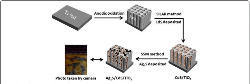
CdS/TNTs were fabricated via the successive ionic layer adsorption and reaction (SILAR) method. The TNTs were dipped inside 0.025 mol · L−1 Cd(NO3)2 and 0.025 mol · L−1Na2S aqueous solutions for 5 min separ-ately and for a couple of cycles. Before dipping into each solution, the nanotube array films were simply rinsed with Milli-Q water and dried in N2 stream. This treat-ment procedure was repeated depending on our need. Ag2S/TNTs were fabricated via similar methods. After being washed in Milli-Q water and dried in N2stream, CdS/TNTs were ready for the Ag2S/CdS/TNTs prepar-ation via SSM. A 0.025 mol · L−1 AgNO3 solution (300μL) was spotted on the local domain of CdS/TNTs with a capillary glass tube (0.5 mm) and dried in air; then, a 0.025 mol · L−1Na2S solution (150μL) was spot-ted on the same place and dried in air. The preparation procedure was repeated a number of times according to requirement. After being washed in ultrapure water, the hybrid nanotube array films were thermally treated at 200 °C for 2 h. The solution used in this work is etha-nol/water solution (ethanol:water = 1:1). The synthesis process of Ag2S/CdS/TNTs by SSM is shown in Fig. 1. Correspondingly, Ag2S/CdS/TNTs was fabricated by uniformly depositing the Ag2S quantum dots into the CdS/TNTs via SILAR method.
Characterizations
Surface morphology of nanotube array films and direct cross section of TNTs thickness measurements were car-ried out using a JEOL JSM-6700F field emission scanning electron microscopy (FE-SEM). The morphology and microstructure of TNTs coupled with CdS and Ag2S.
Photocurrent Measurements
Photocurrent measurements were carried out with a model 263A potentiostat/galvanostat and a three-electrode test cell without applying any bias. The TNTs, CdS/TNTs, Ag2S/TNTs, Ag2S/CdS/TNTs by SSM, and Ag2S/CdS/ TNTs by SILAR method were subsequently used as the working electrode. A platinum wire was used as the coun-ter electrode, and a saturated calomel electrode (SCE) was used as the reference electrode. The measurements were carried out with a 300-W xenon lamp (PLS-SXE300/ 300UV) as light irradiation source. 0.20 mol · L−1Na2S and 0.20 mol · L−1Na2SO3aqueous solutions were used as elec-trolyte with sacrificial agent. The incident photon to current conversion efficiency (IPCE) measurements was performed employing a 150-W Xe lamp coupled with a computer-controlled monochromator. Electrochemical im-pedance spectroscopy (EIS) was performed under illumin-ation with an AC amplitude of 5 mV and frequency range between 100 kHz and 0.1 Hz.
[image:3.595.56.540.89.253.2]Results and Discussion
Figure 2a, b shows the SEM images of the top surface morphologies and a view of cracked TiO2nanotubes an-odized (10 °C) at 60 V for 30 min. It is very clear that the shape of the tubes is quite regular and uniform. The inner diameter of the tubes is about 75 nm, and the wall thickness of the TiO2 nanotubes on top is ~25 nm. As shown in Fig. 2b, TiO2nanotubes pack closely with each other and the TNT length is about 5.5 μm. The SEM images of the top surface morphologies of CdS/TNTs fabricated using successive ionic layer adsorption and re-action (SILAR) method are shown in Fig. 2c. No particle aggregates can be observed at the inlet of the nanotubes, and the surface roughness of the array films rises dra-matically. It may be considered that some CdS nanopar-ticles gather around the tubes. Figure 2d shows the TEM images of the top surface morphologies of the Ag2S/ CdS/TNTs obtained via SSM. As shown in the images, a
small part of the tubes is blocked by the Ag2S particles, which depends on the deposition cycles of Ag2S, and sunlight can still enter the unblocked tubes.
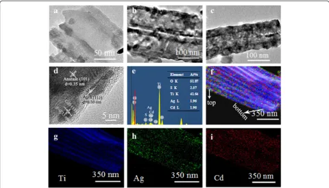
Figure 3 shows the TEM and HR-TEM images of TNTs, CdS/TNTs, and Ag2S/CdS/TNTs by SSM. As seen from the TEM images of fracture surfaces of a TiO2nanotube (Fig. 3a), the inner surface is very smooth. Figure 3b shows that CdS particles get into the TiO2 nanotubes. Unlike Fig. 3a, some particles were introduced inside the nano-tubes. For porous TNTs, the tubes pack closely with each other and CdS did not deposit on the outer wall of the TiO2nanotubes. Figure 3c shows the TEM image of the TiO2nanotubes deposited with CdS and Ag2S. From the TEM images, one can see that there is no obvious differ-ence between Fig. 3c and Fig. 3b HR-TEM images; Fig. 3d shows some particles deposited on the wall of the TiO2 nanotube. Lattice fringes of 0.35 nm were observed in
Fig. 1The synthesis process of Ag2S/CdS/TNTs by SSM
Fig. 2a,bThe SEM images of the top surface morphologies and a view of cracked TiO2nanotubes anodized (10 °C) at 60 V for 30 min.
[image:3.595.306.538.494.664.2]detailed microscopic structures of the TiO2nanotubes, cor-responding to the (101) plane of anatase (JCPDS file no. 71-1167), suggesting that the TiO2nanotubes are well crys-talline structures. The particle diameters are about 6~10 nm inside the TiO2nanotubes, and the lattice fringes are obviously different from the lattice fringes of the TiO2 nanotubes. These particles are CdS or Ag2S. Lattice fringes of 0.30 nm were observed, which corresponds to the (111) plane of the acanthite Ag2S (JCPDS file no. 14-0072), and approximately 0.33 nm corresponds to the (111) plane of the cubic phase of CdS (JCPDS file no. 80-0019). In order to further identify the elemental composition and where CdS and Ag2S particles were deposited, an area of TNTs deposited with CdS and Ag2S is chosen to analyze the cor-responding EDX and EDX elemental mapping. As shown in Fig. 3e, O, S, Ti, Ag, and Cd can be identified. The quan-titative analysis reveals that the atomic composition of O, S, Ti, Ag, and Cd is 51.87, 2.57, 41.64, 1.96, and 1.96 %, re-spectively. With a molar ratio of Ag to Cd at 1:1, we may calculate the molar ratio of Ag2S to CdS at 1:2. We calcu-lated that S should be 2.94 %, which is close to 2.57 % and confirms the formation of Ag2S and CdS. Elemental map-ping of Ag2S/CdS/TNTs-S, Fig. 3f–i, shows that Ag2S and CdS were deposited inside the TiO2nanotubes uniformly.
The composition and crystalline structures of the TNTs, CdS/TNTs, and Ag2S/CdS/TNTs by SSM are also characterized using XRD, and the XRD patterns are
shown in Fig. 4. Figure 4 (a) shows the characteristic dif-fraction peaks of anatase TiO2(JCPDS file no. 71-1167). The diffraction peaks confirm that TiO2 nanotubes are anatase phase after thermal treatment at 450 °C for 2 h. The new weak peaks except the peaks of anatase TiO2 appearing in Fig. 4 (b) are CdS peaks (JCPD file no. 80-0019, marked by C), and these peaks reveal that the CdS particles have the cubic structure. As shown in Fig. 4 (c),
Fig. 3a–iThe TEM and HR-TEM images of TNTs (a), CdS/TNTs (b), and Ag2S/CdS/TNTs by SSM (c,d). EDX spectrum (e) of the Ag2S/CdS/TNTs by SSM (the inset is the table of elements content) and the corresponding EDX elemental mapping (f) of the total elemental mapping of major elements (Ti, Cd and Ag).
[image:4.595.57.538.89.364.2] [image:4.595.305.539.527.685.2]all the diffraction peaks of Ag2S, CdS, and TiO2 are marked with solid circle, solid square, and solid triangle. The peaks of Ag2S attribute to acanthite (JCPDS file no. 14-0072, marked by A). The XRD patterns further con-firm the HR-TEM, EDX, and elemental mapping results.
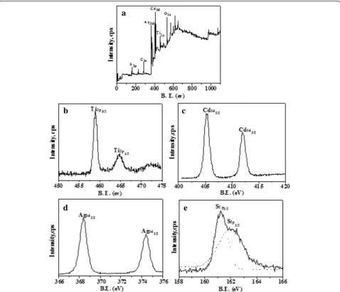
The X-ray photoelectron spectroscopy (XPS) was car-ried out to further confirm the chemical state of Ti, S, Ag, and Cd atoms in the array films of Ag2S/CdS/TNTs by SSM, and each element gives rise to a characteristic set of peaks. The S, C, Ag, Cd, Ti, and O elements can be found in the survey spectrum (Fig. 5a). The C elem-ent is mainly from carbon grid. The high-resolution Ti2p XPS spectrum (Fig. 5b) has two peaks at 464.8 and 458.9 eV, and the doublet feature due to spin-orbit split-ting results in the 2p3/2 and 2p1/2 peaks with spin-orbit
separation 5.9 eV. This result agrees with Ti(IV) in pure anatase TiO2. As shown in Fig. 5c, two characteristic peaks are observed at 405.2 and 412.0 eV, which belong to Cd3d5/2 and Cd3d3/2, respectively. The Ag3d core level could be satisfactorily fit to single spin-orbit pair at 368.4 eV (Ag3d5/2) and at 374.4 eV (Ag3d3/2) in Fig. 5d. Figure 5e is the high-resolution XPS spectrum of S2p, and two peaks have also been given through Gaussian fitting. The two characteristic peaks at 161.2 and 162.2 eV are assigned to S2p3/2and S2p1/2. With reference to the litera-ture [31], the peak S2p1/2at 162.2 eV corresponds to CdS and the peak S2p3/2at 161.2 eV to Ag2S.
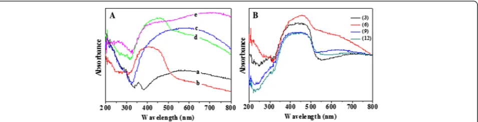
Figure 6a shows the UV-vis absorption spectra of array films of TNTs, CdS/TNTs, Ag2S/TNTs, Ag2S/CdS/TNTs by SSM, and Ag2S/CdS/TNTs via SILAR. The Ag2S/
[image:5.595.59.538.283.694.2]CdS/TNTs via SILAR was produced by depositing Ag2S via SILAR method on the whole film of CdS/TNTs. Both CdS and Ag2S were deposited for 6 cycles. The addition of CdS resulted in an additional absorption band in the UV-vis region (320–530 nm). Compared with TNTs, the absorption of Ag2S/TNTs extends to a longer wave-length up to 800 nm, corresponding to the narrow band-gap of Ag2S (0.9 eV). Both Ag2S/CdS/TNTs by SSM and Ag2S/CdS/TNTs via SILAR show an obvious absorption in light range (320–800 nm), indicating that the Ag2S and CdS deposited onto the TiO2 nanotube arrays can increase the visible light absorption. As shown in Fig. 6a (a), TNTs fabricated by anodic oxidation not only have strong absorption in the UV region but also have a cer-tain degree of absorption in visible range (400–800 nm). When CdS particles were deposited on the TNTs, the absorption of the TNTs was decreased accordingly in visible range (400–800 nm). So, as shown in Fig. 6a (b), CdS/TNTs has a lower absorbance than TNTs under the visible spectrum (500–800 nm). This is also the reason that sample d (Ag2S/CdS/TNTs by SSM) has a lower ab-sorbance than sample c (Ag2S/TNTs) under the visible light spectrum (500–800 nm). Figure 6b shows the UV-vis absorbance of the Ag2S/CdS/TNTs by SSM with dif-ferent deposition cycles of CdS and TiO2, and the ab-sorbance increases firstly and then decreases with the increase of the deposition cycles. The Ag2S/CdS/TNTs by SSM with 6 deposition cycles has stronger absorb-ance in UV-vis range, which indicates that an optimum amount of doping of Ag2S and CdS can benefit the op-tical property of TNTs. At first, the absorption of Ag2S/ CdS/TNTs by SSM under UV-vis regions increased with an increase of Ag2S and CdS particles. But, with further depositing and aggregation of the particles, large parti-cles exhibit increased light scattering [32], so the absorb-ance of Ag2S/CdS/TNTs by SSM then decreased.
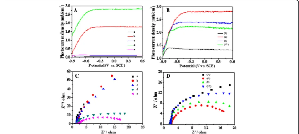
Figure 7a, b shows the photocurrent density (I-V) curves of different array films to evaluate their photo-electric properties. As shown in Fig. 7a, under visible light illumination, TNTs, Ag2S/TNTs, and Ag2S/CdS/
TNTs via SILAR exhibit low photocurrent density, while high photocurrent density values were recorded for CdS/TNTs and Ag2S/CdS/TNTs by SSM. Clearly, Ag2S/ CdS/TNTs by SSM exhibits the highest photocurrent density among the five array films of TNTs, CdS/TNTs, Ag2S/TNTs, Ag2S/CdS/TNTs by SSM, and Ag2S/CdS/ TNTs via SILAR method. The photocurrent density of Ag2S/CdS/TNTs by SSM (2.83 mA/cm2 at 0 V vs. SCE) is much higher than that of TiO2 array films (0.59 mA/cm2). In addition, the onset potentials of all the array films are read directly from the instrument. The onset potentials of TiO2, CdS/TiO2, Ag2S/TiO2, Ag2S/CdS/TNTs via SILAR, and Ag2S/CdS/TNTs by SSM are −0.85, −1.09, −0.89, −0.90, and −1.21 V, re-spectively. The negative shift in onset potential values indicates the decreased surface state densities of the electrodes and increased charge transfer rates at the interface [33], suggesting that Ag2S/CdS/TNTs by SSM has improved photoelectric properties compared with other array films. As shown in Fig. 7b, Ag2S/CdS/ TNTs by SSM with 6 deposition cycles exhibits the largest photocurrent density, and the onset potentials of Ag2S/ CdS/ TNTs by SSM with 3, 6, 9, and 12 deposition cycles
are−0.96,−1.21,−1.09, and−1.05 V, respectively. In order
to investigate the photoelectric properties of the five nano-tube array films further, electrochemical impedance spec-tra (EIS) measurements were carried out using the five films respectively as the working electrodes in 0.20 M Na2S/Na2SO3aqueous solution at the open-circuit poten-tial of the system under visible illumination (λ> 420 nm) with an AC amplitude of 5 mV and frequency range from 100 kHz to 0.1 Hz. The EIS Nyquist plots were shown in Fig. 7c, d. As depicted in Fig. 7c, the diameters of the im-pedance arcs of CdS/TNTs and Ag2S/CdS/TNTs by SSM are smaller than those of TNTs, Ag2S/TNTs, and Ag2S/ CdS/TNTs via SILAR. In the EIS Nyquist plots, the smaller semicircle diameter indicates an effective separ-ation of photogenerated electron-hole pairs and fast inter-facial charge transfer to the electron donor or acceptor. Obviously, the impedance arc of Ag2S/CdS/TNTs by SSM
[image:6.595.61.539.89.211.2]is the smallest among the five films of TNTs, CdS/TNTs, Ag2S/TNTs, Ag2S/CdS/TNTs via SILAR, and Ag2S/CdS/ TNTs by SSM, confirming that the synergy of Ag2S, CdS, and TiO2may decrease the interfacial resistance and in-crease the separation capability of photogenerated electron-hole pairs of Ag2S/CdS/TNTs by SSM. However, Ag2S/TNTs and Ag2S/CdS/TNTs via SILAR have larger semicircle diameters despite a higher absorption capability of visible light. This suggests that uniformly deposited Ag2S on the whole TNTs may increase the recombination capability of photogenerated electron-hole pairs and block the electron transfer to Ti substrate. In addition, as shown in Fig. 7d, the deposition cycles of CdS and Ag2S affect the impedance arc of Ag2S/CdS/TNTs by SSM. Ag2S/ CdS/TNTs by SSM with 6 deposition cycles has the smal-lest semicircle diameter, which suggests that an optimal number of deposition cycles may improve its photoelectric properties obviously. Too much QD deposition will in-crease interfacial resistance and the recombination possi-bility of the photogenerated electron-hole pairs. The EIS results of the different array films correspond to the changing trends of photocurrents and the onset po-tentials (Fig. 7a, b).
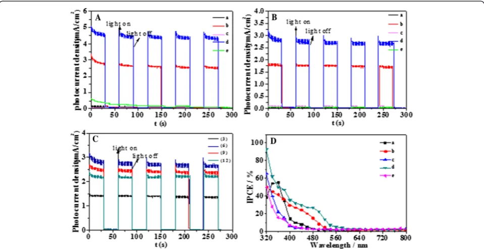
Figure 8a shows the I-tcurves of the five films under intermittent illumination of UV and visible light (320– 800 nm) at bias voltages of 0 V vs. reference electrode Hg/Hg2Cl2. TNTs, CdS/TNTs, Ag2S/TiO2, and Ag2S/ CdS/TNTs by SSM show an instantaneous change in current upon illumination and the current responses in the dark are negligible, indicating that the separation of the electrons and holes of the above four array films is
prompt and the charge transport inside the films is fast. The photocurrent density of Ag2S/CdS/TNTs by SSM (average 4.5 mA/cm2) is higher than that of CdS/TNTs (average 3.0 mA/cm2). Unlike CdS/TNTs and Ag2S/ CdS/TNTs by SSM, the TNTs, Ag2S/TNTs, and Ag2S/ CdS/TNTs via SILAR show very low photocurrent ity values under Xe light irradiation. Photocurrent dens-ity of hybrid Ag2S/CdS/TNTs by SSM is about 37 times higher than that of pure TNTs (average 0.14 mA/cm2). Interestingly, the photocurrent of the array films of Ag2S/ CdS/TNTs via SILAR is very small and decreases gradually, demonstrating that the photoelectrons and holes may re-combine rapidly. These results indicate that more free car-riers are generated and quickly transfer in Ag2S/CdS/TNTs by SSM than in other array films. Figure 8b shows theI-t curves of the five different anodes under intermittent illu-mination of visible light (λ> 420 nm). Similar to Fig. 8a, the photocurrent density of Ag2S/CdS/TNTs by SSM (average 2.8 mA/cm2) and CdS/TNTs (average 1.8 mA/ cm2) is much higher than that of TNTs, Ag2S/TNTs, and Ag2S/CdS/TNTs via SILAR, which indicates lower visible light response of pure TNTs. Figure 8c provides the photo-current response of the array films of Ag2S/CdS/TNTs by SSM with different deposition cycles. Ag2S/CdS/TNTs by SSM with 6 deposition cycles generates the largest photo-current than those of the samples with different deposition cycles. The incident photon to current efficiency (IPCE) test of the five different films (TNTs, CdS/TNTs, Ag2S/ TNTs, Ag2S/CdS/TNTs by SSM, and Ag2S/CdS/TNTs via SILAR) was carried out at 0 V vs. Hg/Hg2Cl2. As shown in Fig. 8d, the photo-response of pure TNTs to the incident
[image:7.595.61.539.90.305.2]light with various wavelengths is principally active in the UV light region. Compared with TNTs, CdS/TNTs and Ag2S/CdS/TNTs by SSM exhibit higher IPCE value, and Ag2S/CdS/ TNTs by SSM shows the high-est photocurrent conversion efficiency at a wavelength range between 320 and 600 nm. However, the IPCE value of Ag2S/TNTs and Ag2S/CdS/TNTs via SILAR is lower than that of TNTs at a wavelength from 330 to 500 nm.
In reference to the mechanism proposed in literatures [34–37], the schematic photovoltaic conversion of Ag2S/ CdS/TNTs by SSM is shown in Fig. 9. The photogener-ated electrons separate from the photogenerphotogener-ated holes
under light irradiation. However, the photogenerated electrons and holes recombine with each other if the electrons cannot be transferred. The conduction band (CB) of the semiconductor (CdS) is located above the CB level of the TNTs, and the photogenerated electrons can transfer from the CB of the CdS to the CB of the ad-jacent TNTs. The electrons flow away through Ti sub-strate and wires rapidly. The valence band (VB) of the TNTs is below that of the adjacent CdS, the photogener-ated holes transfer from the VB of the TNTs to that of the CdS, and the holes transfer to the surface of Ag2S/ CdS/TNTs by SSM. The two factors can reduce the re-combination probability of electrons and holes. The similar transfer process of the photogenerated electrons and holes of Ag2S and TNTS can happen. With a lower bandgap energy (0.9 eV), Ag2S has a wider range of light absorption, and photogenerated electrons and holes are easier to separate than wide-bandgap semiconductors, though they are ready to recombine at the same time, which can be reduced by the interaction between Ag2S, CdS and TiO2. However, the photogenerated electron numbers of Ag2S/CdS/TNTs via SILAR can be reduced because such a large amount of Ag2S uniformly depos-ited on the whole CdS/TNTs may reduce the light ab-sorption of CdS and TNTs. Under irradiation, the photogenerated holes transferred to Ag2S and CdS, which will reduce the stability of Ag2S/CdS/TNTs by SSM in
Fig. 8ATheI-tcurves of the five films under intermittent illumination of UV and visible light (320–800 nm) at bias voltages of 0 V vs. reference electrode Hg/Hg2Cl2.BTheI-tcurves of the five different anodes under intermittent illumination of visible light (λ> 420 nm).CThe photocurrent response of the array films of Ag2S/CdS/TNTs by SSM with different deposition cycles.DThe photocurrent-response of pure TNTs to the incident light with various wavelengths is principally active in the UV light region. TNTs (a), CdS/TNTs (b), Ag2S/TNTs (c), Ag2S/CdS/TNTs by SSM (d), and Ag2S/CdS/TNTs via SILAR (e)
[image:8.595.58.538.89.336.2] [image:8.595.56.292.581.704.2]practical applications. So, 0.20 M Na2S and 0.20 M Na2SO3aqueous solutions were used as electrolyte with sacrificial agent, and the holes in the Ag2S and CdS with active oxidation ability were captured by S2−and S2O32−in the electrolyte (2h++ S2−+ SO32−→ S2O32−) [38], which can enhance the stability of the Ag2S/CdS/TNTs by SSM.
Conclusions
Ag2S/CdS/TNTs by SSM are fabricated via spotting sample method. SEM, TEM, XRD, and XPS results show that most of the CdS and Ag2S can be deposited into the TNTs and some Ag2S particles are deposited on the sur-face of the array films. The Ag2S nanoparticles deposited in the local range of the CdS/TNTs and Ag2S/CdS/TNTs by SSM may widen the absorption spectra of TNTs sig-nificantly to the visible light region and even enhance the absorption of the UV light (320–800 nm). Unlike TNTs, CdS/TNTs, Ag2S/TNTs, and Ag2S/CdS/TNTs via SILAR, Ag2S/CdS/TNTs by SSM have a much larger photocurrent under UV-vis light irradiation. The photo-current density of Ag2S/CdS/TNTs by SSM with an op-timal number of deposition cycles of 6 was about 37 times than that of TNTs under light (320–800 nm) ir-radiation of Xe lamp. With better photoelectric prop-erties and stability of Ag2S/CdS/TNTs by SSM, they have good prospective application in solar energy utilization fields.
Competing Interests
The authors declare that they have no competing interests.
Authors’Contributions
HS did the synthetic and characteristic work in this manuscript. PZ, FZ, and YL gave the advice. JH guided HS for the experimental section and edited the manuscript. All authors read and approved the final manuscript.
Acknowledgements
This work was financially supported by the NSFC (Grant Nos. 21420102006 and 21273134).
Received: 18 May 2015 Accepted: 22 September 2015
References
1. Chen DM, Jiang ZY, Geng JQ, Wang Q, Yang D. Carbon and nitrogen co-doped TiO2with enhanced visible-light photocatalytic activity. Ind Eng Chem Res. 2007;46:2741–6.
2. Choi SK, Kim S, Lim SK, Park H. Photocatalytic comparison of TiO2nanoparticles and electrospun TiO2nanofibers: effects of mesoporosity and interparticle charge transfer. J Phys Chem C. 2010;114:16475–80.
3. Yamauchi M, Abe R, Tsukuda T, Kato K, Takata M. Highly selective ammonia synthesis from nitrate with photocatalytically generated hydrogen on CuPd/ TiO2. J Am Chem Soc. 2011;133:1150–2.
4. Ismail AA, Bahnemann DW. Mesoporous titania photocatalysts: preparation, characterization and reaction mechanisms. J Mater Chem. 2011;21:11686–707. 5. Gong J, Li YH, Hu Z, Zhou ZZ, Deng YL. Ultrasensitive NH3gas sensor from polyaniline nanograin enchased TiO2fibers. J Phys Chem C. 2010;114:9970–4. 6. Du XY, Wang Y, Mu YY, Gui LL, Wang P, Tang YQ. A new highly selective H2
sensor based on TiO2/PtO-Pt dual-layer films. Chem Mater. 2002;14:3953–7. 7. Yang K, Dai Y, Huang B, Whangbo M. Density functional characterization of
the band edges, the band gap states, and the preferred doping sites of halogen-doped TiO2. Chem Mater. 2008;20:6528–34.
8. Khan SUM, Al-Shahry M, Ingler Jr WB. Efficient photochemical water splitting by a chemically modified n-TiO2. Science. 2002;297:2243–5.
9. Pearson A, Bhargava SK, Bansal V. UV-switchable polyoxometalate sandwiched between TiO2and metal nanoparticles for enhanced visible and solar light photococatalysis. Langmuir. 2011;27:9245–52.
10. Shankar K, Mor GK, Fitzgerald A, Grimes CA. Cation effect on the electrochemical formation of very high aspect ratio TiO2nanotube arrays in formamide-water mixtures. J Phys Chem C. 2007;111:21–6. 11. Ramakrishna G, Ghosh HN. Optical and photochemical properties of sodium
dodecylbenzenesulfonate (DBS)-capped TiO2nanoparticles dispersed in nonaqueous solvents. Langmuir. 2003;19:505–8.
12. Chaudhuri RG, Paria S. Visible light induced photocatalytic activity of sulfur doped hollow TiO2nanoparticles, synthesized via a novel route. Dalton Trans. 2014;43:5526–34.
13. Niu P, Hao JC. Fabrication of titanium dioxide and tungstophosphate nanocomposite films and their photocatalytic degradation for methyl orange. Langmuir. 2011;27:13590–7.
14. Potari G, Madarász D, Nagy L, László B, Sápi A, Oszkó A, et al. Rh-induced support transformation phenomena in titanate nanowire and nanotube catalysts. Langmuir. 2013;29:3061–72.
15. Zhou WJ, Du GJ, Hu PG, Li GH, Wang DZ, Liu H, et al. Nanoheterostructures on TiO2nanobelts achieved by acid hydrothermal method with enhanced photocatalytic and gas sensitive performance. J Mater Chem. 2011;21:7937–45. 16. Liao HC, Lee CH, Ho YC, Jao MH, Tsai CM, Chuang CM, et al.
Diketopyrrolopyrrole-based oligomer modified TiO2nanorods for air-stable and all solution processed poly(3-hexylthiophene): TiO2bulk heterojunction inverted solar cell. J Mater Chem. 2012;22:10589–96.
17. Zhao B, Jiang SM, Su C, Cai R, Ran R, Tadé MO, et al. A 3D porous architecture composed of TiO2nanotubes connected with a carbon nanofiber matrix for fast energy storage. J Mater Chem A. 2013;1:12310–20.
18. Myahkostupov M, Zamkov M, Castellano FN. Dye-sensitized photovoltaic properties of hydrothermally prepared TiO2nanotubes. Energy Environ Sci. 2011;4:998–1010.
19. Zwilling V, Darque-Ceretti E, Boutry-Forveille A, David D, Perrin MY, Aucouturier M. Structure and physicochemistry of anodic oxide films on titanium and TA6V alloy. Surf Interface Anal. 1999;27:629–37.
20. Wang DA, Liu LF. Continuous fabrication of free-standing TiO2nanotube array membranes with controllable morphology for depositing interdigitated heterojunctions. Chem Mater. 2010;22:6656–64.
21. Chanmanee W, Watcharenwong A, Chenthamarakshan CR, Kajitvichyanukul P, de Tacconi NR, Rajeshwar K. Formation and characterization of self-organized TiO2nanotube arrays by pulse anodization. J Am Chem Soc. 2008;130:965–74.
22. Zhang ZK, Guo DZ, Xing YJ, Zhang GM. Fabrication of open-ended TiO2 nanotube arrays by anodizing a thermally evaporated Ti/Au bilayer film. Appl Surf Sci. 2011;257:4139–43.
23. Wang DA, Liu Y, Yu B, Zhou F, Liu WM. TiO2nanotubes with tunable morphology, diameter, and length: synthesis and photo-electrical/ catalytic performance. Chem Mater. 2009;21:1198–206.
24. Wang J, Lin ZQ. Dye-sensitized TiO2nanotube solar cells with markedly enhanced performance via rational surface engineering. Chem Mater. 2010;22:579–84.
25. Feng XJ, Sloppy JD, LaTempa TJ, Paulose M, Komarneni S, Bao NZ, et al. Synthesis and deposition of ultrafine Pt nanoparticles within high aspect ratio TiO2nanotube arrays: application to the photocatalytic reduction of carbon dioxide. J Mater Chem. 2011;21:13429–33.
26. Sun WT, Yu Y, Pan HY, Gao XF, Chen Q, Peng LM. CdS quantum dots sensitized TiO2nanotube-array photoelectrodes. J Am Chem Soc. 2008;130:1124–5.
27. Shao ZB, Zhu W, Li Z, Yang QH, Wang GZ. One-step fabrication of CdS nanoparticle-sensitized TiO2nanotube arrays via electrodeposition. J Phys Chem C. 2012;116:2438–42.
28. Li L, Yang XC, Gao JJ, Tian HN, Zhao JZ, Hagfeldt A, et al. Highly efficient CdS quantum dot-sensitized solar cells based on a modified polysulfide electrolyte. J Am Chem Soc. 2011;133:8458–60.
29. Zhang H, Quan X, Chen S, Yu HT, Ma N.“Mulberry-like”CdSe nanoclusters anchored on TiO2nanotube arrays: a novel architecture with remarkable photoelectrochemical performance. Chem Mater. 2009;21:3090–5. 30. Ratanatawanate C, Chyao A, Balkus Jr KJ. S-nitrosocysteine-decorated PbS
31. Hota G, Idage SB, Khilar KC. Characterization of nano-sized CdS-Ag2S core-shell nanoparticles using XPS technique. Colloids Surf A. 2007;293:5–12. 32. Zieli’nska-Jurek A, Wei ZS, Wysocka I, Szweda P, Kowalska E. The effect of
nanoparticles size on photocatalytic and antimicrobial properties of Ag-Pt/ TiO2photocatalysts. Appl Surf Sci. 2015;353:317–25.
33. Yu YX, Ouyang WX, Liao ZT, Du BB, Zhang WD. Construction of ZnO/ZnS/ CdS/CuInS2Core-shell nanowire arrays via ion exchange: p-n junction photoanode with enhanced photoelectrochemical activity under visible light. ACS Appl Mater Interfaces. 2014;6:8467–74.
34. Xie Y, Ali G, Yoo SH, Cho SO. Sonication-assisted synthesis of CdS quantum-dot-sensitized TiO2nanotube arrays with enhanced photoelectrochemical and photocatalytic activity. ACS Appl Mater Interfaces. 2010;2:2910–4. 35. Yang DJ, Liu HW, Zheng ZF, Yuan Y, Zhao JC, Waclawik ER, et al. An efficient
photocatalyst structure: TiO2(B) nanofibers with a shell of anatase nanocrystals. J Am Chem Soc. 2009;131:17885–93.
36. Etgar L, Moehl T, Gabriel S, Hickey SG, Eychmüller A, Grätzel M. Light energy conversion by mesoscopic PbS quantum dots/TiO2heterojunction solar cells. ACS Nano. 2012;6:3092–9.
37. Sarkar S, Moser ML, Tian XJ, Zhang XX, Al-Hadeethi YF, Haddon RC. Metals on graphene and carbon nanotube surfaces: from mobile atoms to atomtronics to bulk metals to clusters and catalysts. Chem Mater. 2014;26:184–95.
38. Daskalaki VM, Antoniadou M, Puma GL, Kondarides DI, Lianos P. Solar light-responsive Pt/CdS/TiO2photocatalysts for hydrogen production and simultaneous degradation of inorganic or organic sacrificial agents in wastewater. Environ Sci Technol. 2010;44:7200–5.
Submit your manuscript to a
journal and benefi t from:
7 Convenient online submission
7 Rigorous peer review
7 Immediate publication on acceptance
7 Open access: articles freely available online
7 High visibility within the fi eld
7 Retaining the copyright to your article