N A N O E X P R E S S
Open Access
Structural and nanomechanical properties of
BiFeO
3
thin films deposited by radio frequency
magnetron sputtering
Sheng-Rui Jian
1*, Huang-Wei Chang
2, Yu-Chin Tseng
1, Ping-Han Chen
2and Jenh-Yih Juang
3Abstract
The nanomechanical properties of BiFeO3(BFO) thin films are subjected to nanoindentation evaluation. BFO thin films are grown on the Pt/Ti/SiO2/Si substrates by using radio frequency magnetron sputtering with various deposition temperatures. The structure was analyzed by X-ray diffraction, and the results confirmed the presence of BFO phases. Atomic force microscopy revealed that the average film surface roughness increased with increasing of the deposition temperature. A Berkovich nanoindenter operated with the continuous contact stiffness
measurement option indicated that the hardness decreases from 10.6 to 6.8 GPa for films deposited at 350°C and 450°C, respectively. In contrast, Young's modulus for the former is 170.8 GPa as compared to a value of 131.4 GPa for the latter. The relationship between the hardness and film grain size appears to follow closely with the Hall–Petch equation.
Keywords:BiFeO3thin films, XRD, AFM, Nanoindentation, Hardness
Background
Multiferroic materials exhibit some unique characteristics with the co-existence of at least two kinds of long-range ordering among ferroelectricity (or antiferroelectricity), ferromagnetism (or antiferromagnetism), and elasticity. Single-phase compounds in which both ferro-magnetism and ferroelectricity arise independently and may couple to each other to give rise to magneto-electric interactions are ideal materials for novel functional device applications but are unfortunately rare in nature [1]. BiFeO3(BFO) is one of the most important multiferroic
materials so far discovered, which has a ferroelectric Curie temperature of 1,103 K [2,3] and an antiferromagnetic Néel temperature of 643 K [4]. In addition to its interest-ing optical properties [5], strong couplinterest-ing between ferro-electric and magnetic orders is observed in BFO at room temperature, making it a strong candidate for realizing room-temperature multiferroic devices [6,7]. However, while most of the researches have been concentrated on the abovementioned magneto-electric characteristics of
BFO, researches on the mechanical characteristics of this prominent functional material have been largely ignored. In particular, since the mechanical properties of materials are size-dependent, the properties obtained from thin films may substantially deviate from those of the bulk ma-terial. In view of the fact that most practical applications of functional devices are fabricated with thin films, it is de-sirable to carry out precise measurements of the mechan-ical properties of BFO thin films.
Because of its high sensitivity, excellent resolution, and easy operation, nanoindentation has been widely used for characterizing the mechanical properties of various nanoscale materials [8,9] and thin films [10-12]. Among the mechanical characteristics of interest, the hardness, Young's modulus, and the elastic/plastic deformation be-haviors of the interested material can be readily obtained from nanoindentation measurements. For instance, by analyzing the load–displacement curves obtained during the nanoindentation following the methods proposed by Oliver and Pharr [13], the hardness and Young's modu-lus of the test material can be easily obtained. In general, in order to avoid the complications arising from the sub-strate material, the contact depths of the indenter need to be less than 10% of the film thickness to obtain
* Correspondence:[email protected] 1
Department of Materials Science and Engineering, I-Shou University, Kaohsiung 840, Taiwan
Full list of author information is available at the end of the article
intrinsic film properties [14]. On the other hand, it is very difficult to obtain meaningful analytical results for indentation depths less than 10 nm because of the equipment limitations. Hence, for films thinner than 100 nm, it is almost impossible to obtain results without be-ing influenced by responses from the substrate. In order to gain some insights on the substrate influences and obtain the intrinsic properties for films thinner than 100 nm, it is essential to monitor the mechanical properties as a function of depth. Herein, in this study, a conti-nuous stiffness measurement (CSM) mode [15] was adopted to continuously monitor the hardness and Young's modulus values of BFO films as a function of the indentation depth. Variations in mechanical proper-ties for BFO thin films deposited under different condi-tions are discussed in conjunction with the crystalline structure, grain size, and surface morphology of the re-sultant films.
Methods
The BFO thin films investigated in this study were deposited on Pt/Ti/SiO2/Si(100) substrates at the
depos-ition temperatures of 350°C, 400°C, and 450°C, respect-ively. The deposition process was conducted in a radio frequency magnetron sputtering system, and a commer-cially available Bi1.1FeO3 pellet was used as the target.
The base pressure of the sputtering chamber was better than 1 × 10⁻⁷ Torr. During deposition, a mixed gas of Ar/O2 = 4:1 with a total pressure was introduced, and
the input power was maintained at 80 W. All of the BFO thin films are about 200 nm thick. The compos-ition of the film was identified by an energy-dispersive X-ray analysis and double checked by X-ray fluorescence analysis. The crystal structure of BFO thin films was an-alyzed by X-ray diffraction (X'Pert XRD, PANalytical B. V., Almelo, The Netherlands; CuKα,λ = 1.5406 Å). The surface features were examined by atomic force micros-copy (AFM; Topometrix-Accures-II, Topometrix Cor-poration, Santa Clara, CA, USA). The root mean square of the surface roughness, RRMS, was calculated by the
following equation [16]:
RRMS¼
ffiffiffiffiffiffiffiffiffiffiffiffiffiffiffiffiffi 1
N
XN
n¼1
r2
n v u u
t ð1Þ
Here N is the number of data and rn is the surface height of thenth datum.
Nanoindentation experiments were preformed on a MTS Nano Indenter® XP system (MTS Nano Instru-ments, Knoxville, TN, USA) with a three-sided pyram-idal Berkovich indenter tip by using the CSM technique [15]. This technique is accomplished by imposing a small, sinusoidal varying force on top of the applied
linear force that drives the motion of the indenter. The displacement response of the indenter at the excitation frequency and the phase angle between the force and displacement are measured continuously as a function of the penetration depth. Solving for the in-phase and out-of-phase portions of the displacement response gives rise to the determination of the contact stiffness as a con-tinuous function of depth. As such, the mechanical properties changing with respect to the indentation depth can be obtained. The nanoindentation measure-ments were carried out as follows: First, prior to apply-ing loadapply-ing on BFO thin films, nanoindentation was conducted on the standard fused silica sample to obtain the reasonable range (Young's modulus of fused silica is 68~72 GPa). Then, a constant strain rate of 0.05 s−1was maintained during the increment of load until the in-denter reached a depth of 60 nm into the surface. The load was then held at the maximum value of loading for 10 s in order to avoid the creep which might signifi-cantly affect the unloading behavior. The indenter was then withdrawn from the surface at the same rate until the loading has reduced to 10% of the maximum load. Then, the indenter was completely removed from the material. In this study, constant strain rate was chosen in order to avoid the strain-hardening effects. At least 20 indentations were performed on each sample, and the distance between the adjacent indents was kept at least 10μm apart to avoid interaction.
In nanoindentation tests, the hardness is defined as the applied indentation load divided by the projected contact area as follows:
H¼Pmax
Ap ð2Þ
where Ap is the projected contact area between the
in-denter and the sample surface at the maximum indenta-tion load,Pmax. For a perfectly sharp Berkovich indenter,
the projected area Ap is given by Ap ¼24:56h2c with hc
being the true contact depth.
The elastic modulus of the sample can be calculated based on the relationships developed by Sneddon [17]:
S¼2βEr ffiffiffiffiffiffiAp
p
=pffiffiffiπ. HereSis the contact stiffness of the material, andβis a geometric constant withβ= 1.00 for the Berkovich indenter, respectively. The reduced elastic modulus,Er, can be calculated from the following
equa-tion:
1
Er¼
1−v2 film
Efilm þ
1−v2 i
Ei ð3Þ
Herevis Poisson's ratio, and the subscripts i and f de-note the parameters for the indenter and the BFO thin films, respectively. For the diamond indenter tip, Ei =
BFO thin films in this work. It is generally accepted that the indentation depth should never exceed 30% of the film thickness to avoid the substrate effect on hardness and modulus measurements [18]. Our samples and test methodology were considered as adequate based on this concept. In addition, because of the fact that it enters as
1−v2 film
in the calculation ofE, an error in the estima-tion of Poisson's ratio does not produce a significant ef-fect on the resulting value of the elastic modulus of thin films [19].
Results and discussion
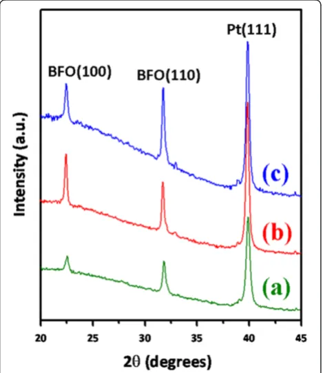
Figure 1 shows the XRD results of BFO thin films obtained with deposition temperatures of 350°C, 400°C, and 450°C, respectively. It is evident that the intensity and the full width at half maximum (FWHM) of the BFO(110) diffraction peak are both improved with the increasing deposition temperature, indicating a tendency of better film crystallinity and increased grain size. The grain size, D, can be estimated according to Scherrer's equation [20]:
D¼B0:9λ
cosθ ð4Þ
whereλ, B, andθare the X-ray wavelength, the FWHM of the BFO(110) diffraction peak, and the corresponding Bragg's diffraction angle, respectively. The estimated
grain sizes for BFO thin films deposited at 350°C, 400°C, and 450°C are 24.5, 30.6, and 51.2 nm, respectively. As can be seen below, consistent results were obtained from the AFM examinations.
As shown in Figure 2, the AFM observations reveal that the RRMS values for BFO thin films deposited at
350°C, 400°C, and 450°C are 6.5, 9.4, and 14.8 nm, re-spectively. Moreover, as shown in Figure 2a,b,c, the BFO thin films all exhibit similar dense, homogeneous micro-structures, albeit that the grain size appears to increase with increasing deposition temperature. The average grain size obtained from image analysis on the AFM im-ages indeed gave consistent results with those obtained from XRD analyses. Namely, the microstructure of BFO films are polycrystalline, and the grain size increases from about 24.5 nm for thin films deposited at 350°C to about 51.2 nm for thin films deposited at 450°C. This is attributed to the additional thermal energy acquired from higher deposition temperature, which may further facilitate the coalescence of the adjacent grains (or nu-clei) and result in larger grains during deposition process.
Figure 3a displays the typical load–displacement (P-h) curves for the BFO film deposited at 350°C, which re-flects the general deformation behavior during the pene-tration of a Berkovich indenter loaded with the CSM mode. The P-h response obtained by nanoindentation contains information about the elastic behavior and plas-tic deformation and thus can be regarded as the ‘ finger-print’ of the properties of BFO thin films. The curve appears to be smooth and regular. The absence of any discontinuities along either the loading or unloading seg-ment is in sharp contrast to those observed in GaN thin films [21,22] and in single-crystal Si [23,24], indicating that neither twinning nor pressure-induced phase trans-formation is involved here.
[image:3.595.57.292.435.706.2]Figure 3b,c presents the hardness and Young's modu-lus versus penetration depth curves for the BFO film de-posited at 350°C, 400°C, and 450°C, respectively. The curves can be roughly divided into two stages, namely, an initial increase to a maximum value followed by a subsequent decrease to a constant value. The initial sharp increase in hardness at a small penetration depth is usually attributed to the transition from purely elastic to elastic/plastic contact. Only under the condition of a fully developed plastic zone does the mean contact pres-sure represent the hardness. When there is no plastic zone, or only a partially formed plastic zone, the mean contact pressure measured according to the Oliver and Pharr method [13] is usually smaller than the nominal hardness. After the first stage, the hardness decreases in a rather meandering manner, presumably involving massive dislocation and grain boundary activities relevant to the fine grain structure of the films. Nevertheless, the Figure 1XRD patterns of BFO thin films deposited at various
fact that it eventually reaches a constant value at a moder-ate indentation depth indicmoder-ates that a single mmoder-aterial is be-ing measured. The hardness values obtained at this stage, thus, can be regarded as the intrinsic properties of the films. The penetration depth dependence of Young's modulus (Figure 3c) behaves similarly as that of the hard-ness. Consequently, both mechanical parameters were de-termined using the curves obtained from the CSM loading scheme (Figure 3b,c) by taking the average values within the penetration depth of 40 to 60 nm. This range of pene-tration depth was chosen intentionally to be deep enough for observing plastic deformation during indentation yet Figure 2AFM images of BFO thin films deposited at various
[image:4.595.58.290.90.689.2]deposition temperatures.(a) 350°C, (b) 400°C, and (c) 450°C, respectively.
to be shallow enough to avoid the complications arising from the effects of surface roughness [25] and substrate [18]. Table 1 summarizes the hardness and Young's modu-lus for various BFO thin films obtained from different de-position methods and indentation operation modes.
It is well known that the dependence of material hard-ness on the grain size can be described by the phenom-enological‘Hall-Petch’equation [27]:
H Dð Þ ¼H0þkHPD−1=2 ð5Þ
where H0 and kH-P are denoted as the lattice friction
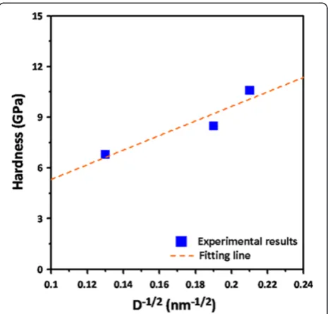
stress and the Hall–Petch constant, respectively. A plot of the hardness versus D−1/2data for BFO thin films de-posited at various temperatures is displayed in Figure 4. We note that although the grain size of BFO thin films remains relatively small as compared to that of the usual metallic materials, the data still follow pretty closely to the Hall–Petch relation, and the so-called negative Hall– Petch effect [28] is not observed here. The dashed line represents the fit to the Hall–Petch equation for the ex-perimental data, which gives
H Dð Þ ¼1:03þ43:12D−1=2 ð6Þ
which indicates a probable lattice friction stress of 1.03 GPa, and the Hall–Petch constant of 43.12 GPa nm1/2 for BFO thin films also indicates the effectiveness of the grain boundary in hindering the dislocation movements.
Furthermore, it is evident that both the hardness and Young's modulus of BFO thin films decrease monotonic-ally with increasing deposition temperature. The corre-sponding hardness values (Young's modulus) are 10.6 (170.8), 8.5 (147.6), and 6.8 (131.4) GPa for BFO thin films deposited at 350°C, 400°C, and 450°C, respectively. Since the higher deposition temperature leads to the lar-ger grain size for BFO thin films, as we have discussed previously, it is reasonable to consider that the decrease of hardness and Young's modulus might be mainly due to the grain size effect [29].
Conclusion
In conclusion, we have carried out the XRD, AFM, and nanoindentation techniques to investigate the fundamental
nanomechanical properties and their correlations with the microstructural features of the technologically important multiferroic BFO thin films. The XRD analysis showed that BFO thin films were equiaxial polycrystalline in nature, al-beit that the predominant (110) orientation and a rougher surface morphology were gradually developed with increas-ing deposition temperature. Nanoindentation results indi-cated that, depending on the grain size which is intimately related to the deposition temperature, BFO thin films have hardness ranging from 6.8 to 10.6 GPa and Young's modu-lus ranging from 131.4 to 170.8 GPa with the higher values corresponding to lower deposition temperatures. In addition, the hardness of BFO thin films appears to follow the Hall–Petch equation rather satisfactorily, and the Hall– Petch constant of 43.12 GPa nm1/2suggests the effective-ness of grain boundary in inhibiting the dislocation move-ment in BFO thin films.
Competing interests
The authors declare that they have no competing interests.
Authors' information
SRJ is an associate professor and YCT is a designated topic student (in the Department of Materials Science and Engineering, I-Shou University, Kaohsiung, Taiwan). HWC is an associate professor and PHC is a master student (in the Department of Applied Physics, Tunghai University, Taichung, Taiwan). JYJ is a professor (in the Department of Electrophysics, National Chiao Tung University, Hsinchu, Taiwan).
Authors’contributions
[image:5.595.306.539.88.310.2]SRJ designed the project of experiments; performed the XRD, AFM, and nanoindentation analyses; and drafted the manuscript. YCT dealt with the experimental data. HWC and PHC carried out the growth of BFO thin films, and JYJ participated in the paper discussion. All authors read and approved the final manuscript.
Table 1 Hardness and Young's modulus of BFO thin films obtained from various deposition methods
H(GPa) E(GPa)
Radio frequency magnetron sputtering-derived BFOa
350°C 6.8 131.4
400°C 8.5 147.6
450°C 10.6 170.8
Sol–gel-derived BFO [26] 2.8~3.8 26~51 a
[image:5.595.57.292.642.725.2]The present work.
Acknowledgments
This work was partially supported by the National Science Council of Taiwan under grant no. NSC101-2221-E-214-017. JYJ is partially supported by the NSC of Taiwan and the MOE-ATU program operated at NCTU.
Author details
1Department of Materials Science and Engineering, I-Shou University, Kaohsiung 840, Taiwan.2Department of Applied Physics, Tunghai University, Taichung 407, Taiwan.3Department of Electrophysics, National Chiao Tung University, Hsinchu 300, Taiwan.
Received: 28 April 2013 Accepted: 11 June 2013 Published: 25 June 2013
References
1. Hill NA:Why are there so few magnetic ferroelectrics?J Phys Chem B
2000,104:6694.
2. Neaton JB, Ederer C, Waghmare UV, Spaldin NA, Rabe KM:First-principles study of spontaneous polarization in multiferroic BiFeO3.Phys Rev B2005, 71:014113.
3. Simões AZ, Aguiar EC, Gonzalez AHM, Andrés J, Longo E, Varela JA:Strain behavior of lanthanum modified BiFeO3thin films prepared via soft chemical method.J Appl Phys2008,104:104115.
4. Catalan G, Scott JF:Physics and applications of bismuth ferrite.Adv Mater
2009,21:2463.
5. Wei J, Xue D, Xu Y:Photoabsorption characterization and magnetic property of multiferroic BiFeO3 nanotubes synthesized by a facile sol–gel template process.Scripta Mater2008,58:45.
6. Kim HH, Dho JH, Qi X, Kang SK, Macmanus-Driscoll JL, Kang DJ, Kim KN, Blamire MG:Growth and characterization of BiFeO3 film for novel device applications.Ferroelectrics2006,333:157.
7. Vasudevan RK, Liu Y, Li J, Liang WI, Kumar A, Jesse S, Chen YC, Chu YH, Nagarajan V, Kalinin SV:Nanoscale control of phase variants in strain-engineered BiFeO3.Nano Lett2011,11:3346.
8. Ni H, Li XD, Gao H:Elastic modulus of amorphous SiO2nanowires.
Appl Phys Lett2006,88:043108.
9. Ni H, Li XD, Cheng G, Klie R:Elastic modulus of single-crystal GaN nanowires.J Mater Res2006,21:2882.
10. Jian SR, Juang JY, Chen NC, Jang JSC, Huang JC, Lai YS: Nanoindentation-induced structural deformation in GaN/AlN multilayers.Nanosci Nanotechnol Lett2010,2:315.
11. Jian SR, Ku SA, Luo CW, Jang JY:Nanoindentation of GaSe thin films.
Nanoscale Res Lett2012,7:403.
12. Jian SR, Lin YY, Ke WC:Effects of thermal annealing on the structural, electrical and mechanical properties of Al-doped ZnO thin films deposited by radio-frequency magnetron sputtering.Sci Adv Mater2013, 5:7.
13. Oliver WC, Pharr GM:An improved technique for determining hardness and elastic modulus using load and displacement sensing indentation experiments.J Mater Res1992,7:1564.
14. Tsui TY, Pharr GM:Substrate effects on nanoindentation mechanical property measurement of soft films on hard substrates.J Mater Res1999, 14:292.
15. Li XD, Bhushan B:A review of nanoindentation continuous stiffness measurement technique and its applications.Mater Charact2002,48:11. 16. Miyoshi K, Chung YW:Surface Diagnostics in Tribology: Fundamental
Principles and Applications.Singapore: World Scientific Publishing; 1993. 17. Sneddon IN:The relation between load and penetration in the
axisymmetric Boussinesq problem for a punch of arbitrary profile.
Int J Eng Sci1965,3:47.
18. Li XD, Gao H, Murphy CJ, Caswell KK:Nanoindentation of silver nanowires.
Nano Lett2003,11:1495.
19. Hu LJ, Zhang XW, Sun Y, Williams RJJ:Hardness and elastic modulus profiles of hybrid coatings.J Sol–gel Sci Tech2005,34:41.
20. Cullity BD, Stock SR:Element of X-Ray Diffraction.New Jersey: Prentice Hall; 2001:170.
21. Jian SR:Berkovich indentation-induced deformation behaviors of GaN thin films observed using cathodoluminescence and cross-sectional transmission electron microscopy.Appl Surf Sci2008,254:6749. 22. Jian SR, Ke WC, Juang JY:Mechanical characteristics of Mg-doped GaN
thin films by nanoindentation.Nanosci Nanotechnol Lett2012,4:598.
23. Bradby JE, Williams JS, Wong-Leung J, Swain MV, Munroe P:Transmission electron microscopy observation of deformation microstructure under spherical indentation in silicon.Appl Phys Lett2000,77:3749.
24. Jian SR, Chen GJ, Juang JY:Nanoindentation-induced phase transformation in (110)-oriented Si single crystals.Curr Opin Solid State Mater Sci2010,14:69.
25. Bobji MS, Biswas SK, Pethica JB:Effect of roughness on the measurement of nanohardness-a computer simulation study.Appl Phys Lett1997, 71:1059.
26. Sen P, Dey A, Mukhopadhyay AK, Bandyopadhyay SK, Himanshu AK: Nanoindentation behavior of nano BiFeO3.Ceram Int2012,38:1347. 27. Venkatraman R, Bravman JC:Separation of film thickness and
grain-boundary strengthening effects in Al thin-films on Si.J Mater Res
2040,1992:7.
28. Conrad H, Narayan J:On the grain size softening in nanocrystalline materials.Scripta Mater2000,42:1025.
29. Delobelle P, Guillon O, Fribourg-Blanc E, Soyer C, Cattan E, Rèminens D: True Young modulus of Pb(Zr, Ti)O3films measured by nanoindentation.
Appl Phys Lett2004,85:5185.
doi:10.1186/1556-276X-8-297
Cite this article as:Jianet al.:Structural and nanomechanical properties of BiFeO3thin films deposited by radio frequency magnetron sputtering.Nanoscale Research Letters20138:297.
Submit your manuscript to a
journal and benefi t from:
7Convenient online submission 7Rigorous peer review
7Immediate publication on acceptance 7Open access: articles freely available online 7High visibility within the fi eld
7Retaining the copyright to your article