2017 2nd International Conference on Information Technology and Management Engineering (ITME 2017) ISBN: 978-1-60595-415-8
Regional RFID Based Dual-Frequency Positioning System
Pei-rong WANG, Xiao-dong CHENG
*and Hui-yuan LIU
College of Electronic Information Engineering, Inner Mongolia University, Hohhot, 010021, China
*Corresponding author
Keywords: Dual frequency positioning, Low frequency activation, RSSI.
Abstract. Considering the features of indoor positioning, this paper represents a regional RFID based dual-frequency positioning system. The mode, this paper intends to present, of waking up at low frequency of 125KHZ and transmitting at high of 433MHZ, makes it possible to realize the better communication and be adapted to the complex regional environment. The testing proves that, in the indoor complicated environment, the system can keep working steadily, and, with increased the number of antennas, that the positioning precision can reach less than 20cm and accuracy more than 96%.
Introduction
More precise positioning information is needed to improve the service quality, implement resources integration and ensure the public security in large scale and complex indoor environment. Indoor RFID positioning technology [1], as a supplement of outdoor positioning technology of GPS or Beidou navigation system has been extensively applied in various fields.
Organization of the Text
System Design
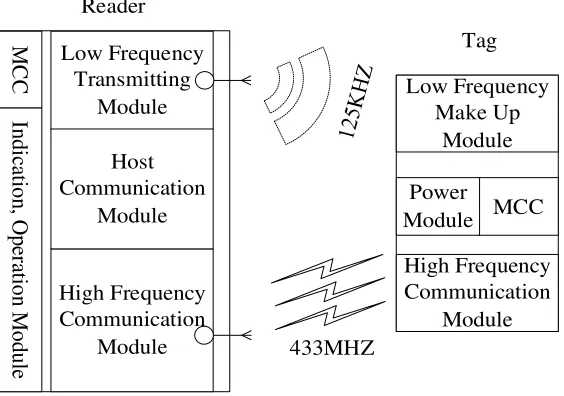
The system adopts dual-frequency positioning mode. To begin with, the reader transmits low frequency signal at 125KHZ constantly by low frequency active antenna. The semi-active electronic tag, if falling into the excitation range of low frequency signal, will be woken up by the active signal and starts to work, being followed by transmitting data at 433MHZ to reader that receives the information and sends it to PC terminal with primary processing. The useful processed information will be displayed on PC or sent to cloud platform. The client can review the data via mobile terminal APP. The system framework is as shown in Figure 1.
Tag
Active Antenna Reader
Ether Net Controller PC Terminal Cloud
Platform Mobile
Terminal
Positioning Region A
Positioning Region B
...
Server
Activation Region
Figure 1. System Architecture.
M
C
C Low Frequency Transmitting
Module
High Frequency Communication
Module Host Communication
Module MCC
Low Frequency Make Up
Module
High Frequency Communication
Module Power Module
433MHZ
In
d
ic
at
io
n
, O
p
er
at
io
n
M
o
d
u
le
Reader
[image:2.612.167.449.75.273.2]Tag
Figure 2. Blocks of Reader and Tag Communication.
Reader Design
As the controlling part of dual frequency system, reader mainly consists of micro control unit, RF processing module, low frequency transmitting module, communication module, power module and other accessories [3].
With the processing capacity and cost being taken into consideration, STM32F103 is selected as the core processor of micro controller. The advantage, of low power consumption at modes of sleep, safe shutdown, standby, is the main factor for choosing the microprocessor, besides its high reliability.
In accordance with the actual need as well as the stability and reliability of the equipment, the communication module, composed of W5500 network chip and RJ-45(HR911105) network transformer, primarily accomplishes the communication with host computer. W5500 chip is embedded ether net controller utilizing all hardware TCP/IP protocol stack, which enables the embedded system to access the net easily via SPI interface. With complete TCP/IP protocol stack, 10/100Mbps ether net media access control (MAC) and physical (PHY), W5500 is fairly suitable for the clients who need microcontrollers to realize the internet functions.
CC1101 is chosen as the RF processing chip. Being a real single-chip UHF transceiver with low cost. The circuit adopts 433MHZ frequency band of CC1101, integrated with a high configurable modem that supports various modulation formats with data signaling rate of 500kbps. CC1101, in terms of hardware, offers the extensive assistance to data packet processing, data cache, burst data transfer,clear channel assessment, link quality indication and electromagnetic wave excitation. CC1101 communicates with host control via SPI interface, adopting ISO/IEC 1800-7 air interface protocol.
Table 1. Frame Format Wake Up Signal.
Carrier
Brust Preamble Wake Up Pattern
Data Bit
Reader No. Active
Antenna No.
The output waveform of simulation by software is as show in Figure 3.
Figure 3. The Output Waveform of 125KHZ Signal Simulation.
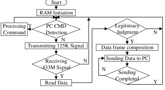
Due to much load, reader is complex in aspect of software designing. Firstly, the initial configuration of each module can be done by host control that sets up communication interface of RJ-45 or RS232 with PC and initializes the setting of the timer and host PC. Secondly, at low frequency of 125KHZ, by controlling the timer, the wake up signal data generates which is transmitted through a polling mode. Finally, when the high frequency receiving module receives the signal sent from the tag, the reader will process the signal information and transmit it to PC terminal, then enter into the next cycle. The flow chart is shown as in Figure 4.
Start
RAM Initiation
PC CMD Detection
Transmitting 125K Signal
Receiving 433M Signal
Read Data
Legitimacy Judgment
Data frame composition
Sending Data to PC
Sending Completed Processing
Command
Y N
Y
N
N
N
Y
[image:3.612.99.508.123.295.2]Y
Figure 4. Flow Chart of Reader.
Electronic Tag Design
Tag, as a mobile device, is mainly attached to people or mobile object. It is primarily composed of micro control unit, high frequency transmitting module, low frequency wake-up receiving module and power module.
Micro control unit utilizes 20 pin chip of MSP430G2553. MSP430G2553 has 8 Channel 10 bit analog to digital converter (ADC), on-chip comparator, touch type enable I/O port, universal serial communication interface, 16K flash memory and 512b RAM as well as 4 types of calibration frequencies and 16MHz internal frequency. The circuit is tremendously simplified. Owing to five power saving modes, it can be rapidly waken up from standby in less than 1us.
[image:3.612.146.459.406.578.2]Design in this way makes the electronic tag smaller in size.
Low frequency wake-up receiving module uses AS3933 chip from AMSCO (Austria Micro System AG). AS393, a low frequency wake-up receiver with 3 channels, is able to wake up and receive ASK signals from 3 channels. The receiver is able to receive signals ranging from 15 KHz to 150 KHz, and supports programmable data rate and Manchester decoding with clock recovering. Meanwhile, it provides automatic tuner with built-in antenna and RSSI value for various channels. Thereof, the low frequency antenna, composed of inductance, capacitance and resistance, makes use of parallel resonant mode. The PREMO 3DC11LP-0720J three-dimensional orthogonal antenna is employed to avoid the receiving directivity of low frequency. The inductance in all directions is 7.2mH. To achieve the best low frequency receiving sensitivity, the theoretical computation of resistance-capacitance of resonant circuit matching is performed. When L=7.2mH,F=125KHZ; C=225.3867PF is obtained. The design is short of capacitance of 225.3867pF, so capacitances of 220pF and 5.6pF are paralleled for substitution. The capacitance resonant circuit within AS3933 can be materialized through internal programming, with step size ranging from 1pF to Maximum 31pF.The performance of low frequency antenna is closely associated with its quality factor Q. Generally speaking, the higher the Q value is, the longer distance of low frequency wake-up can function. However, if the Q value is too high, it will cause transmission bands to decrease and ultimately affect the accuracy of the data. The typical Q value in this design is 15, R=84.78 Ω. Due to the simplified design of hardware circuit, AS3933 adopts internal crystal oscillator that is configured and verified by internal program. The 3 receiving channels are connected with XYZ pins of the 3D low frequency antenna respectively.
Firstly, configure the clock in AS3933 through the SPI in MCU, and setup other working registers to realize low frequency wake-up to receive data. The working mode of AS3933 is shown as in Figure 5. Thereof, the design uses ON/OFF mode. When Scan mode is turned on, channel 1,2 and 3 will be switched on, using 32 as its pattern and the wake-up frequency set between 59 to 150KHz. AS3933 utilizes ASK to modulate without gain reduction. Set preamble check value to 0x3AC3 and R6 register to 16-bit pattern format complied to be 16-bit Manchester code. When, such tested factors as 125KHZ low frequency carrier brust, preamble and pattern, are up to the setup requirements, the WAKE pin of AS3933 generates a high level signal followed by the output Manchester clock pulse from CLDAT pin to restore wave pattern, and output Manchester decoding date from DAT pin.
Start RSSI
(WAKE=0)
Start RSSI
(WAKE=1) Interception
Mode
(WAKE=0)
Relevant Mode
(WAKE=0)
Data Receiving
(WAKE=1) Frequency Found, No
Mode Established
Unmatching Mode
Eliminate Wake-Up Zone Bit or Overtime
Matching Mode
Figure 5. AS3933 Working Mode.
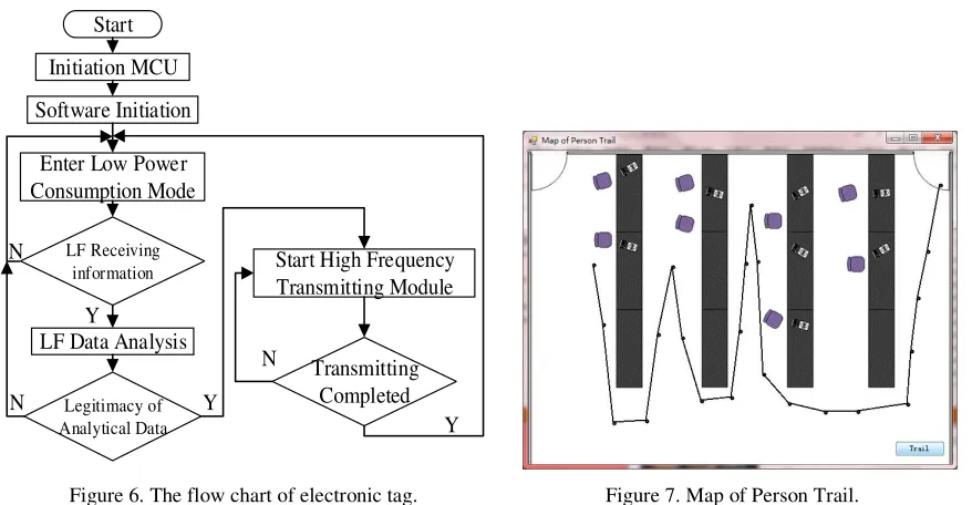
Start
Initiation MCU
Software Initiation
Enter Low Power Consumption Mode
LF Receiving information
LF Data Analysis
Legitimacy of Analytical Data
Start High Frequency Transmitting Module
Transmitting Completed N
Y N
N Y
[image:5.612.96.535.66.294.2]
Y
Figure 6. The flow chart of electronic tag. Figure 7. Map of Person Trail.
Tag uses 3.3V lithium battery as power supply. To achieve low power consumption, the high frequency module, powered by BL1551 switch module, controls BL1551 via the host control chip to realize on and off of the voltage of high frequency part. This design adopts lithium polymer (lipo) battery that is a kind of chemical battery. Compared with other batteries, it is high in energy, small in size and light in weight. Due to the ultrathin characteristics, lipo can be designed with different form factors and capacities, having minimum thinness of 0.5mm. Laminated soft package is commonly utilized in its manufacturing process, so it is convenient and flexible to change its size leading to scores of models. In short, lipo can fully meet the requirements of making electronic tags. Application Software Design and Scenario Application. In the system upper layer, C# language is applied in Visual Studio for software programming and communication controlling. The system is made up of three modules: RFID information capture module, positioning information processing module and human computer interaction module. In the data processing system, both historical database and real-time database are designed, via SQL Server database to fulfill the data management. The database includes layout configuration information, historical position information RSSI, location body, devices (reader and tag) information, and clients information for the purpose of accomplishing real-time monitoring and historical path inquiry. In line with the rational layout of the region area, reader and active antenna can complete precise positioning on certain body [4]. Human positioning tracing is shown as in Figure 7.
In addition, this system can be applied in such scenarios as access control, meeting signature etc., among which the access control system is shown as in Figure 8.
activated Area 1
activated Area 2
Enter Exit
Low Frequency Activator Reader
Processing Center
Tag Attached to Person
Figure 8. Access Control Application Model.
[image:5.612.195.423.571.685.2]from the tag will be, through the exchange center, transmitted to the management center for further statistical analysis related.
Summary
In a nutshell, the mode, this paper intends to present, of waking up at low frequency of 125KHZ and transmitting at high of 433MHZ, makes it possible to realize the better communication and be adapted to the complex regional environment. It is of reliable precision, excellent stability and perfect implantation in variety of scenarios. Beside, RSSI based mode combining distance measurement, neighbor algorithm and three points positioning algorithm have the deployment accomplished flexibly in various scenarios. The dominating advantage shows from small rang, critical path to key area. In the aspect of regional positioning, the innovation and highly raised accuracy of the system make it believed to be worth study and promotion.
References
[1] R Want. An introduction to RFID technology [J].IEEE Pervasive Computing, 2006, 5(1).
[2] Zuo Y J. Survivable RFID systems: issues, challenges and techniques [J]. IEEE Trans Syst, Man Cybern Part C: Appl Rev, 2010, 40(4): 406-418.
[3] Kerem Kapucu and Catherine Dehollain. A Passive UHF RFI D Platform for Sensing Applications [C]. Advance in Sencors and Interfaces. 2015, 146-151.