© 2017, IRJET | Impact Factor value: 5.181 | ISO 9001:2008 Certified Journal
| Page 3235
Study of Three State Switching Cell Based
DC-To-DC Converter
P.ManojBharath
1,Dr.K.Subramanian
21
Assistant Professor, Shri Sitheswarar Engineering College,
Arcot – 632 503, Vellore District, Tamil Nadu. India
2
Associate Professor, Dept. of Energy And Power Electronics, School of Electrical Engineering
VIT University, Vellore, Tamil Nadu, India, 632014
---***---Abstract— Needs of variable dc power supply increased due to industrial growth. Variable speed induction motor drives are widely used in most of the industries by using V/F control technique. In order to meet the high energy level of d.c supply for those drives three-phase diode rectifier followed by the dc-to-dc converters employed for that with high energy level. Buck-boost operation of dc-to-dc converter employed in emerging application such as photovoltaic cell or fuel cell as a dc source for a vehicle drives with high gain dc voltage. This paper investigate the performance of a dc-dc converter consists of high gain voltage multiplier. It is three state switching cells of capacitors. A 1kW prototype model of dc-to-dc converter is fabricated and tested. Computer simulation of this scheme completed using the power system toolbox built-in libraries of MATLAB / SIMULINK software. The results are presented
.
Key words:switching cell, dc-to-dc converter, voltage multiplier
I.
Introduction
At present, implementations of power electronics circuit based variable speed drives in most of industries are essential, to increase the quantity of industrial products and to fulfill the work force shortage advanced technology implementation is essential. Modern power electronic device and its controls are compact therefore; it reduces the space requirement of the new and old industries. Moreover distributed power generators, which are generate the electrical power from non-conventional energy sources like wind, photovoltaic cell etc, have to be interface with grid supply needs high level variable dc supply[1]-[5].
Buck-boost operations of dc-to-dc converters are widely used for low and medium level drives applications. Conventional boost converters are insufficient for high applications, due to its switching at high-level voltage ratings and small duty cycles. Coupled inductors boost converter approach presented in details [6], coupled inductor and switched capacitor scheme without extra windings presented by Yi-Pin Hsieh et al [7]. The same technique implemented in sustainable energy system [8].The design, analyses and losses calculation of those converters are describing analytically and verified experimentally presented in detail [9] - [10].
In the last few years, the converter based on three state switching cells (3SSC) has been proposed, development of this converters reported by different authors [11]-[14]. The aim of this work is experimental study on a three-state switching cell based voltage multiplier, incorporate in buck-boost operation of a DC-DC converter. The forthcoming section-2 describes the system configuration of three-state cell based dc-to-dc development. Matlab based simulation of the circuit discussed in section 3, section 4 explain the experimental work carried out. Simulated and experimental results are discussed in section -5, conclusion presented in section 6.
II.System Configuration
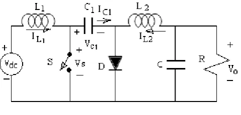
[image:1.595.310.550.541.656.2]A.Cuk mode operation of dc-dc converter The CUK converter, Fig.1, named after its inventor, is similar to the buck-boost regulator, to regulate output voltage is greater or less than the input voltage depends on the input voltage magnitude but the polarity of the output voltage is in opposite to input [15]. The advantage of the topology is a continuous current at both the input and the output of the converter and needs high number of reactive components and high current stresses on the switch, diode, and the capacitor C1.
Fig. 1 CUK dc –to-dc converter
Dc to dc regulator operation of CUK converter, Fig.1, consist of DC input voltage source , energy transfer capacitor , controlled switch , inductor , filter capacitor ‘C’, and load resistance ‘R’.
© 2017, IRJET | Impact Factor value: 5.181 | ISO 9001:2008 Certified Journal
| Page 3236
discharged to the inductor L2 and the capacitor ‘C1’ charging
[image:2.595.81.246.157.470.2]If the switch‘S’off and diode is on. Those currents and voltage across the inductors are shows in Fig.2. However, average voltages across the inductors are zero.
Fig. 2 output voltage and current waveforms Therefore, the DC voltage transfer function of the cuk converter is [15],
It is same as the buck-boost regulator. The boundaries between the continuous and discontinuous conduction mode of inductor L1 and L2 are obtained by,
Where f is the switching frequency, D is the duty cycle, R is the load resistance, Lb1 and Lb2 are the inductors
B.Voltage Multiplier
Figure 3, show the voltage multiplier consist of ‘n’ number of capacitor unit. Proper gating of the switches can change the effective capacitance. In order to reduce the switching transient diode is connected across the switch individually, Fig.3.
The advantages are input current is continuous with low ripple, the input inductor is designed for twice the switching frequency, with consequent weight and volume reduction, the voltage stress across the switches is lower than half of the output voltage, and naturally clamped by one output filter capacitor.
Fig. 3 voltage multiplier circuit
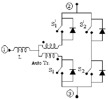
C.Three State Switching Cell
The association of two two-state switching PWM cells interconnected to a center-tapped autotransformer, from which a family of dc–dc converters can be derived, obtains three state solid switching (3SSC) operations. The advantages are
reduced size, weight, and volume of magnetic, which are designed for twice the switching frequency,
the current stress through each main switch is equal to half of the total output current rating, losses are distributed among the semiconductors, leading to better heat distribution
Consequently more efficient use of the heat sinks
[image:2.595.373.507.268.463.2]© 2017, IRJET | Impact Factor value: 5.181 | ISO 9001:2008 Certified Journal
| Page 3237
Fig. 4 Three state switching cell
D. Proposed System
[image:3.595.270.541.356.719.2]The proposed three-state switching cell based d.c-to-d.c converter comprises of voltage multiplier, Fig.3, and three-state switching cell, Fig.4, is shown in Fig.5. It is designed with high voltage gain with less ripple currents flow through the inductor. The inductor values designed with consideration of twice the switching frequency so that its size is reduced.
Fig. 5 Proposed three-state switching cell based d.c-to-d.c converter
The voltage stress through the switches is less than half of the output voltage due to clamping performed by the output filter capacitor. It is also important to mention that, for a given duty cycle, the output voltage can be increased by adjusting the transformer turns ratio without affecting the voltage stress across the main switches. Metal oxide semiconductor field-effect transistors (MOSFETs) with reduced turn on-resistance used to minimize conduction losses further.
III. Matlab based simulation
The proposed dc-to-dc converter circuit, Fig.5, is rigged up MATLAB / SIMULINK software [16] by using built-in libraries of power system toolbox and simulation completed for 5milli seconds, Fig.6. Simulation data are shows in Appendix.
For the regulated voltage of 134V as a output voltage, input voltages are chosen randomly, for example of 40V and 80V are considered as an input for boost and buck operation respectively. Theregulation study completed for 100Ω load resistance. The simulated results are shows in Figs.8 and 9.
.
[image:3.595.64.275.405.713.2]© 2017, IRJET | Impact Factor value: 5.181 | ISO 9001:2008 Certified Journal
| Page 3238
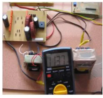
IV. Experimental work [image:4.595.321.557.92.273.2]In order to study the system experimentally, hardware is designed, constructed and tested in the laboratory is shown in Fig. 7.
Fig. 7 Photo of an experimental setup V. result and discussion
[image:4.595.79.257.151.321.2]Figure 8 illustrates the load voltage (2.661x50 = 133.05V) and current (1.325A) waveforms of three-state switching cell based dc-to-dc converter operated in boost mode with input voltage of 40 volts.
Fig. 8 simulated load voltage and current boost operation
Figure 9 illustrates the load voltage (2.661x50 = 133.05V) and current (1.325A) waveforms of three-state switching cell based dc-to-dc converter operated in boost mode with input voltage of 80 volts.
[image:4.595.323.514.311.428.2]Fig. 9 simulated load voltage and current buck operation
Table 1 Specifications of dc-to-dc converter
VI. Conclusion
A high voltage multiplier based three-state cell developed and incorporated with dc-to-dc converter is simulated in MATLAB/ Simulink software and tested in the laboratory for load of 100Ω resistance.
The regulation study completed for 40V and 80V as input voltage to maintain 134V output. Further investigation on closed loop control is in progress.
References
[1] Amjadi,Z. and Williamson, S.S., “Power-electronics-based solutions for plug-in hybrid electric vehicle energy storage and management systems”, IEEE Trans. on Indus. Elect., vol.57, No. 2, 2010, pp. 608–616.
[2] Yi-Ping Hsieh, Jiann Chen, Tsorng-Juu Liang and Lung-Sheng Yang, “ A Novel High Step-Up DC-DC converter for micro grid System”, IEEE Trans. On Power Elect. vol. 26, No. 4, 2011, pp. 1127-1136.
[3] Berkhout, M. and Dooper, L., “Class-D audio amplifiers in mobile applications”, IEEE Trans. On Circuits Systems- I, vol. 57, No. 5, 2010, pp. 992–1002.
[4] Chen, S. Liang, T. Yang, L. and Chen, “A cascaded high step-up dc–dc converter with single switch for micro
Load resistance 100 Ω
L1, L2 70μH
C 120 µfd
C1,C2 1.5 µfd
C3,C4 3 µfd
C5,C6 4.5 µfd
[image:4.595.62.275.409.584.2]© 2017, IRJET | Impact Factor value: 5.181 | ISO 9001:2008 Certified Journal
| Page 3239
source applications”, IEEE Trans. on Power Electronics., vol. 26, no. 4, 2011, pp. 1146–1153.
[5] Abutbul, O. Gherlitz, A. Berkovich, Y. and Ioinovici, A “Boost converter with high voltage gain using a switched capacitor circuit,” in proceedings of the International Symposium Circuits Systems, 2003, pp. III-296–III-299. [6] Su man Dwari and Leila Parsa, “ A novel high Efficiency High power interleaved Coupled-Inductor boost DC-DC converter for Hybrid and Fuel Cell Electric vehicle”, Proceeding of 2007 IEEE vehicle Power and Propulsion Conference, University of Texas, Arlington, 2007, pp. 998- 1007.
[7] Yi-Ping, Jain-Fuh Chen, Tsorng-Juu Liang and laung-Sheng Yang, “Novel high Step-Up DC – DC Converter With Coupled Inductor and Switched Capacitor techniques”, IEEE trans. on Indus. Electronics, vol. 50, No.2, 2012, pp. 399- 404.
[8] Yi-Ping, Jain-Fuh Chen, Tsorng-Juu Liang and laung-Sheng Yang, “Novel high Step-Up DC – DC Converter With Coupled Inductor and Switched Capacitor techniques for sustainable Energy System”, IEEE trans. on Indus. Electronics, vol. 26, No.12, 2011, pp. 3481- 3490
[9] Y.P. Hsieh, J.F. Chen, T. J. Liang and L.S. Yang, “Analysis and Implementation of novel single-switch step-up DC-DC converter”, IET Power Electron., Vol. 5. No. 1, 2012, pp. 11-21.
[10] Liangzong He and Jiazhi Lei, “High Step-Up Converter with Passive Lossless Clamp Circuit and Switched-Capacitor: Analysis, Design, and Experimentation”, Proceeding of 28th Annual IEEE Applied Power Electronics Conference and Exposition (APEC), 2013, Fort Worth, TX USA, pp.2070- 2077.
[11] Araujo, S. V. Torrico – Bascope, R. P. Bascope, G. V. and Menezes, L, “Step-up converter with high voltage gain employing three state switching cell and voltage multiplier”, Power Electronics Specialists Conference, 2008, pp. 2271–2277.
[12] Araujo, S.V. Torrico-Bascope, R.P. and Torrico-Bascope, G. V, “Highly efficient high step-up converter for fuel-cell power processing based on three-state commutation cell,” IEEE Trans. on Indus. Electronics., vol. 57, no. 6, 2010, pp. 1987–1997.
[13] Balestero, J. P. R. Tofoli, F. L. Fernandes, R. C. and Seixas, F. J.M, “Power factor correction boost converter based on the three-state switching cell”. IEEE Trans. on Indus. Electronics., vol. 59, no. 3, 2012, pp. 1565–1577.
[14] Da Camara, R. A. Cruz, C. M. T., and Torrico -Bascope, R. P, “Boost based on three-state switching cell for UPS applications,” Proceedings of Brazilian Power Electronics Conference., 2009, pp. 313–318.
[15] Ned Mohan, Tore M. Undeland and William P. Robbin, “Power Electronics” John Wiley & Sons, InC, Singapore, 1985, pp. 184-187
[16] Mat lab/Simulink Software Version.9.0.