Doutreloigne Jan
Centre for Microsystems Technology (CMST), Interuniversity Microelectronics Centre (IMEC) and University of Gent, Gent, Belgium
Email: [email protected]
Received 7 August 2014
Abstract
This paper describes how the power efficiency of fully integrated Dickson charge pumps in high- voltage IC technologies can be improved considerably by implementing charge recycling tech-niques, by replacing the normal PN junction diodes by pulse-driven active diodes, and by choosing an appropriate advanced smart power IC technology. A detailed analysis reveals that the combi-nation of these 3 methods more than doubles the power efficiency compared to traditional Dick-son charge pump designs.
Keywords
Charge Recycling, Dickson Charge Pump, High-Voltage Generator, Power Efficiency Optimization, Smart Power Technology
1. Introduction
Fully integrated charge pumps are used in a wide variety of applications, going from flash memories over dedi-cated display drivers to MEMS actuator drivers. Some applications ask for specific features, such as high current drive capability or very good output voltage stability. But for all of them, good overall power efficiency is of the utmost importance.
Achieving high power efficiency in fully integrated Dickson charge pumps is not straightforward due to the fact that integrated capacitors exhibit considerable parasitic capacitance to the substrate, resulting in a dramatic efficiency drop. In this paper, charge recycling techniques are presented to substantially reduce this negative ef-fect. Replacing the standard PN junction diodes by pulse-driven DMOS transistors acting as almost ideal active diodes is another method to enhance the power efficiency. Finally, the choice of an appropriate smart power IC technology with superior transistor and integrated capacitor performance also helps to boost the efficiency. In this paper, these 3 methods are described and compared.
2. Basic Dickson Charge Pump Design
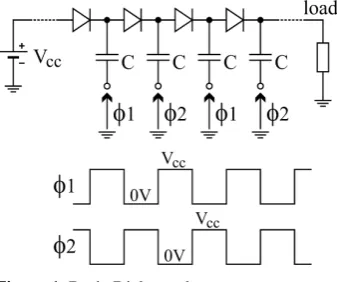
Figure 1. Basic Dickson charge pump.
tive stages are driven by 2 complementary clock signals. Charge is transferred from one capacitor to the next at the rhythm of the clock, yielding an output voltage that can be much higher than the input voltage. In a real ap-plication, a feedback control loop is added to the circuit in order to maintain the output voltage very stable and independent of system parameters or load characteristics. This can be achieved by continuously adjusting the clock frequency of the charge pump.
A major issue in integrated Dickson charge pumps is the fact that the integrated capacitors exhibit a large pa-rasitic capacitance between their bottom plate and the normally grounded substrate of the chip, as illustrated in Figure 2.
The parasitic capacitance Cp does not contribute to the useful operation of the circuit, but it does affect the power consumption in a negative way. Indeed, the parasitic capacitance Cp is connected directly to the output of the clock buffers, and these buffers have to charge and discharge this parasitic capacitance constantly, resulting in additional power losses inside the transistors of the clock buffers, without having any useful impact on the circuit operation. The consequence is an extremely poor power efficiency of typically 10% to 20% in case of a voltage transformation ratio of 20, even when conventional design strategies for efficiency improvement are ap-plied [2]-[4]. It is obvious that special measures have to be taken in order to boost the efficiency to a more ac-ceptable level. The following 3 sections describe the 3 proposed techniques to achieve this goal.
3. Charge Recycling
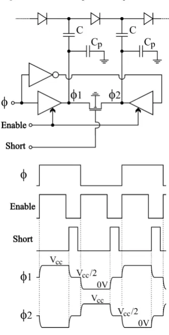
A first approach to mitigate the power losses related to the parasitic capacitance Cp is to employ the dedicated charge recycling technique of Figure 3. In this configuration, the normal clock buffers are replaced by 3-state buffer circuits. Before switching the clock buffers from one state to the next (from 0V to the supply voltage Vcc, or vice versa), their outputs are disabled (high-impedance output) during a very short time interval and the buf-fer outputs are short-circuited by means of an additional MOSFET. As a result, half of the charge that was stored on the parasitic capacitance Cp of a particular stage will be transferred to the parasitic capacitance of the next stage. Consequently, this parasitic capacitance of the next stage does not have to be charged anymore from 0V to Vcc when its clock buffer is again enabled, but only from Vcc/2 to Vcc. This technique yields a 50% reduction of the clock buffer power consumption that is related to the parasitic capacitance in each stage, and hence, it boosts the power efficiency effectively.
4. Pulse-Driven Active Diodes
Figure 3. Charge recycling principle.
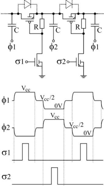
A first possibility would be to replace the standard PN junction diodes by Schottky diodes that exhibit a much lower threshold voltage. Unfortunately, high-performance Schottky diodes are not readily available in most smart power IC technologies. An interesting alternative is to replace the diodes by properly driven transistors that provide a low-resistance path during the charge transfer between capacitors of consecutive stages. In the ideal situation, the charge transfer can be completed to its full extent during the conduction time of the transistor, meaning that the equivalent VT value would simply be 0V, resulting in maximum power efficiency! A possible practical implementation of this active diode approach is shown in Figure 4.
[image:3.595.211.379.187.519.2]Figure 4. Pulse-driven active diodes.
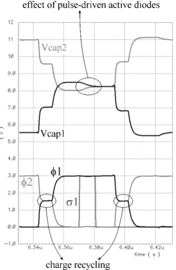
charge transfer to continue until the top plates of the 2 capacitors reach exactly the same electric potential. This corresponds to the ideal situation of VT = 0 V, meaning that the P-type DMOS transistors act like almost ideal active diodes. The effect of this technique is clearly illustrated in the simulation result of Figure 5, where Vcap1 and Vcap2 are the electric potentials of the capacitor top plates in consecutive stages. The reduction of the 0.5 V voltage drop (the VT of the built-in drain-bulk diode) to 0 V when the P-type DMOS device is activated by the σ1 pulse is very clear in this simulation. Also note the previously described charge recycling in the clock sig-nals.
Although this technique looks very simple and attractive, the practical implementation and the correct com-ponent dimensioning are not straightforward at all and require a careful optimization process.
5. Proper IC Technology Choice
The third method to increase the power efficiency deals with a proper choice of IC technology. Of course, the specified maximum output voltage of the Dickson charge pump will set a lower limit for the high-voltage han-dling capability of the smart power IC technology, but also the performance of the integrated capacitors and transistors are very important selection criteria. Indeed, competitive technologies with similar voltage ratings may offer different capacitor structures with completely different values of the parasitic capacitance, resulting in significantly different power efficiency levels. Also the specific performance (on-state resistance as well as pa-rasitic capacitance) of the P-type and N-type high-voltage DMOS transistors in the pulse-driven active diode circuit of Figure 4 will largely affect the overall power efficiency.
Figure 5. Simulation of the pulse-driven active diodes.
Figure 6. Poly-N+ capacitor (PN capacitor).
Figure 7. Poly1-poly2 capacitor (PP capacitor).
dling capability of the smart power IC technology, but also the performance of the integrated capacitors and transistors are very important selection criteria. Indeed, competitive technologies with similar voltage ratings may offer different capacitor structures with completely different values of the parasitic capacitance, resulting in significantly different power efficiency levels. Also the specific performance (on-state resistance as well as pa-rasitic capacitance) of the P-type and N-type high-voltage DMOS transistors in the pulse-driven active diode circuit of Figure 4 will largely affect the overall power efficiency.
To illustrate the importance of the capacitor structure, we’ll consider the example of the 100 V 0.7 µm I2T technology (Intelligent Interface Technology) of ON Semiconductor. Figures 6-8 show a vertical cross section of 3 different kinds of integrated capacitors in this technology. Figure 6 depicts a capacitor between a poly-sil- icon layer at the top and a highly doped N+ implantation at the bottom, with a very thin dielectric in between. Figure 7 represents a capacitor structure between 2 poly-silicon layers, with a somewhat thicker dielectric. Fi-nally, Figure 8 shows a sandwich structure where the shorted poly-silicon and metal2 layers form 2 capacitors in parallel towards the metal1 layer. The dielectric in this structure is considerably thicker than in the 2 previous cases.
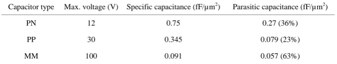
Based on the information from Table 1, we can easily select the most appropriate capacitor type for every in-dividual stage in the Dickson charge pump. In the first set of stages, where the capacitor operating voltage is li-mited to values below 30 V, the PP capacitor is selected as it is superior in terms of percentual parasitic capacit-ance. However, for the last stages with operating voltages in excess of 30 V, the MM capacitor is the only option because of the voltage rating. The very bad corresponding percentual parasitic capacitance towards the substrate is then something we have to live with and it means that for charge pumps with an output voltage much higher than 30 V, the overall power efficiency of the generator will be very low!
For charge pumps with very high output voltages it is therefore advisable to compare several smart power IC technologies and to select the one that offers a type of high-voltage capacitor with the lowest possible percentual parasitic capacitance towards the substrate. Take for instance the 80 V I3T technology (Improved Intelligent In-terface Technology) of ON Semiconductor, which is much more advanced than the 100 V I2T technology as it is based on a 0.35 µm CMOS core process instead of the older 0.7 µm process. Due to the fact that this 80 V I3T technology allows much smaller metal track widths and spacings as well as 5 metal levels instead of only 2, it becomes possible to integrate multi-metal capacitors with a kind of staggered “finger”-structure design of the 2 electrodes as shown in the schematic cross-sectional view of Figure 9.
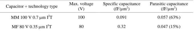
[image:6.595.126.470.655.721.2]This type of capacitor design makes optimal use of the horizontal and vertical dimensions (there is capacit-ance between neighboring metal stripes in horizontal and vertical direction) to get the maximum capacitcapacit-ance for a given amount of silicon area while keeping the parasitic capacitance towards the substrate to a minimum. This is clearly evidenced in Table 2, comparing the performance of the metal1-metal2-poly capacitor (MM) in the 100 V 0.7 µm I2T technology and the multi-metal “finger” capacitor (MF) in the 80 V 0.35 µm I3T technology. As could be expected, the high-voltage MF capacitors in the 80 V 0.35 µm I3T technology exhibit a 4 times lower percentual parasitic capacitance than the high-voltage MM capacitors in the 100 V 0.7 µm I2T technology. This makes the 80 V 0.35 µm I3T technology the preferred choice for integrating high-voltage Dickson charge pumps with maximum power efficiency.
Table 1. Comparison of different capacitor types in the 100 V 0.7 µm I2T technology.
Capacitor type Max. voltage (V) Specific capacitance (fF/µm2) Parasitic capacitance (fF/µm2)
PN 12 0.75 0.27 (36%)
PP 30 0.345 0.079 (23%)
Figure 9. Multi-metal capacitor with staggered “finger”-structure design (MF capacitor).
Table 2. Comparison of capacitor performance between the 100 V 0.7 µm I2T and 80 V 0.35 µm I3T technologies.
Capacitor + technology type Max. voltage (V) Specific capacitance (fF/µm2) Parasitic capacitance (fF/µm2)
MM 100 V 0.7 µm I2
T 100 0.091 0.057 (63%)
MF 80 V 0.35 µm I3T 80 0.32 0.047 (15%)
When comparing smart power IC technologies, also differences in high-voltage transistor structures and tran-sistor characteristics may be observed. As an example, Table 3 compares the same 100 V 0.7 µm I2T and 80V 0.35 µm I3T technologies in terms of specific on-state resistance of the main high-voltage P-type and N-type DMOS transistors. It is clear from this table that the high-voltage DMOS devices in the 80 V 0.35 µm I3T tech-nology have a roughly 3 times lower on-state resistance, which means that the duration of the control pulses σ1 and σ2 for activating the level-shifters in the pulse-driven active diode circuit of Figure 4 can be chosen much shorter than in the case of the 100 V 0.7 µm I2T technology, resulting in less power dissipation inside the level- shifters, and hence, improved overall power efficiency.
From the discussions of Table 2 and Table 3, we conclude that a careful comparison and selection of smart power IC technologies is of the utmost importance to achieve the maximum power efficiency in integrated high-voltage Dickson charge pumps!
6. Impact of the 3 Proposed Techniques
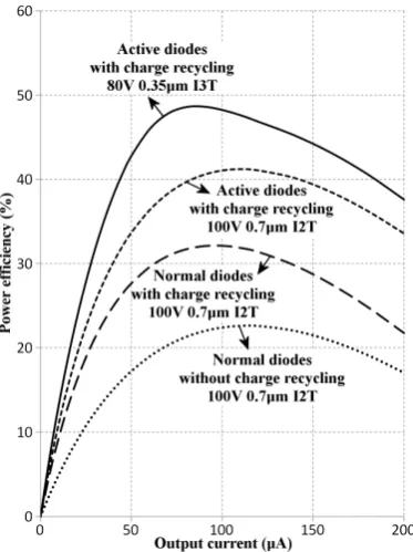
To illustrate the effect of the 3 techniques we proposed for boosting the power efficiency of integrated high- voltage Dickson charge pumps, a comparison is made for 1 specific application: a monolithic driver chip for a 60 V bistable nematic Liquid Crystal Display (LCD). For that purpose an integrated Dickson charge pump is needed, capable of transforming a 3 V supply voltage into a 60 V output voltage with a maximum output current rating of 200 µA. In every design (i.e. for each implementation of the proposed techniques), a clock frequency of 10 MHz and a capacitor of 12 pF in each stage of the charge pump were assumed, and the number of stages was chosen in such a way that the specified 60 V output voltage was within reach for the maximum output cur-rent value of 200 µA. The results of this comparative study can be observed in Figure 10, showing the power efficiency as a function of the output current for several design cases.
[image:7.595.128.469.292.348.2]Figure 10. Impact of the 3 proposed techniques on the power effi-ciency versus output current characteristic.
Table 3. Comparison of high-voltage transistor performance between the 100 V 0.7 µm I2T and 80 V 0.35 µm I3T technologies.
Technology Transistor type Max. voltage (V) Specific on-state resistance (Ωmm2)
100 V 0.7 µm I2
T N-type DMOS 100 0.76
P-type DMOS 90 1.32
80 V 0.35 µm I3T N-type DMOS 80 0.26
P-type DMOS 80 0.47
7. Conclusion
Three methods for increasing the power efficiency of fully integrated Dickson charge pumps were presented and analyzed: the use of charge recycling techniques, the replacement of standard PN junction diodes by pulse-dri- ven active diodes, and the use of an advanced smart power IC technology with high-performance integrated high-voltage capacitors and transistors. Data from specific design cases provide a clear proof of the positive im-pact of these 3 methods. It is shown that the power efficiency is more than doubled compared to traditional Dickson charge pump configurations.
References
[1] Dickson, J.F. (1976) On-Chip High-Voltage Generation in MNOS Integrated Circuits Using an Improved Voltage Multiplier Technique. IEEE Journal of Solid-State Circuits, 11, 374-378.
http://dx.doi.org/10.1109/JSSC.1976.1050739
[2] Di Cataldo, G. and Palumbo, G. (1996) Design of an N-th Order Dickson Voltage Multiplier. IEEE Transactions on Circuits and Systems-I: Fundamental Theory and Applications, 43, 414-417.
http://dx.doi.org/10.1109/81.502213
[3] Palumbo, G., Pappalardo, D. and Giabotti, M. (2002) Charge-Pump Circuits: Power-Consumption Optimization. IEEE Transactions on Circuits and Systems I: Fundamental Theory and Applications, 49, 1535-1542.
[4] Palumbo, G., Pappalardo, D. and Giabotti, M. (2001) Modeling and Minimization of Power Consumption in Charge Pump Circuits. Proceedings of the 2001 IEEE International Symposium on Circuits and Systems (ISCAS), 402-405.
[image:8.595.130.470.400.465.2]