F-75
PROGRAMMED DATA
PROCESSOR-7
USERS- HANDBOOK
PREFACE
This handbook concerns programming and operating the Programmed Data Processor-7, a high speed, stored program, digital computer manufactured by the Digital Equ.ipment Corporation. Section 1 presents a summary of the standard computer system and the available options, as well as information on the notation used throughout the handbook. Section 2 presents a brief block-diagram discussion of the standard computer system and its maior logic elements. Sections 3 and 4 are devoted to explaining the structure and organization of the instructions, and providing information on the basic use of the equipment by features. Sections 5 throughout 12 describe the stand-ard peripheral equipment and the optional equipment in functional groups.
Section
2
CONTENTS
SYSTEM INTRODUCTION •
. .
.
.
.
.
.
.
.
.
.
.
.
. .
.
.
. . .
. .
.
.
.
.
. . .
.
.
. .
Computer Organization...
Processor ••••••••
.
... .
Core Memory , ••••••••••••••••.•••••••••••••••••••••••
I
n"terface ••.••••.•••••••.•••..•••.•••.•.•••.•.•.••.••Input/Output
...
Processor Options
...
Core Memory Options •..•.••..••..••...••..•Input/Output Options , •••...•....•....•...•.•
Programming System
'FORTRAN Compi ler
Sym bo lie Assem bier
Digital Debugging Tape (DDT)
Symbolic Tape Editor, •..•••••••••••••••••.••••••••••••
Bus-Pak II •...•...
Symbols ••••••••
FUNCTIONAL DESCRIPTION
...
Processor ••••••••••••
Accumulator (AC)
Link (L) •..•...•...
Memory Address Register (MA) ••....•...••...•
Program Counter (PC) •••.••..•....•....•...•...••.••
Memory Buffer Register (MB) ••..•...•••••.•..•...•....•
Instruction Register (lR) •..•••..•••.•••••
Maior State Generator ••.•••••••••••••••
Detailed Processor Block Diagram Discussion
Core M'emory
...
Interface ••••••••••.••••.••••.
... .
4
4
5
5
6
6
7
8
12
12
13
13
13
13
14
15
15
15
16
16
16
16
16
17
18
CON TEN T S (continued)
Section
2 (continued) Device Selector (OS) ... 23
Information Distributor (I D) • • • . . • • . • . . . .. . .. . . • • • . . • . . .. • 25
Information Collector (lC) •..•... , •••...••..• ,. . . . • .. 25
Input/~Output .. • • .. • • .. • .. • • • .. • • • . . . • . . . . • . . . • • .. 26
3
I NSTRUCTI ONS...
27Memory Reference Instructions ... -. • • • • • • • . • • • • . .. • • 27
Augmented Instructions .... '. .. • • .. .. .. .. .. • • • .. .. .. .. • .. • .. .. .. .. .. • .. .. .. .. • .. • • 31
Input/Output Transfer Instructions ... 31
Operate Instructions ... 32
4
BASIC MACHINE LANGUAGE PROGRAMMING ... .39
Memory Addressing ...
39
Indirect Addressing ... ,. ....•....•..•...• .-. . . • . . . . • •
39
Auto-Indexing ... ,. • • . .. . • • 40
Arithmetic Operations •....•.. , . . . • • . • .. • . . . .. • • • • • . • . . • • . .. 42
Complement Arithmetic ... '. • . • •• .. . ... .... ••• 42
Addition ••..••.•.••..•....••••••..•.••..•..•.••.•.•• 43
Subtraction ... 44
Multiplication and Division ... ~... 44
Input/Output Fundamentals ••.••• ;... 44
Program Flags ... ' •• ~... 44
Input/Output Status ••.•••..•. . . . • • . . . • • • • . . • • . . . .. •
45
Input/Output Skip Facil ity (I/OS) • . • . . . • .. •
45
Input/Output Trap. . . . .. . . • . . . .• • • . . . • • •• 46
Program Interrupt Control (PI<;:) ...
47
Real Time Clock ... . . .. .. . . . . • . . . • . . . • • . . • • . • • . • . . . • • • 49
Section
5
6
7
8
CON TEN T S (continued)
PROCESSOR OPTIONS •...••••..••...•.••.•. 0 • • • • • • • • • • • • 52
Extended Arithmetic Element Type 177 •.•••• 0 • • • • • • • 0 • • • • • • • 0 52
EAE Microprogramming •..••• 0 0 . . . 0 . 0 • • • • • 0 0 • • 0 • • • • • 0 . • • 58
EAE Programm i ng Exampl es • ~ ...••..• 0 • • • • • • • • • • • • • • • • • • 61
Automatic Priority Interrupt Type 172 0 • • • • • • • • • • • • • • • • • • • • • • • 64
The Multi-Instruction Subroutine Mode
The Single Instruction Subroutine Iv\ode
Priori ty Interrupt Instructi ons •.••••.••••. 0 • • • • 0 • 0 0 0 0 0 • • •
Data Interrupt Mu Itiplexer Control Type 173 •...•.•..••. 0 •
CORE MEMORY OPTIONS •....•...•.•. 0 • • • • • • • 0 0 0 • • • • • • • •
o.
Memory Extension Control Type 148 ••.••.•....•. ~ ....••.... '.
Core Memory Iv\odules Type 147 and 149 •...••... 0 • 0 • • 0 . . .
STANDARD INPUT/OUTPUT EQUIPMENT •....•.... 0 . 0 . 0 0 • • • • • • • '
65
66
67
68
71
71
73
75
Teletype Model
33
KSR and Control Type 649 ...• 0 • • • • • • 0 • • 0 • • ' 75Keyboard ••••••••..• 0 • • • • • • • 0 0 • • • • 0 • • • • • • 0 • • • • • • • • 0 • • 75
Teleprinter •••..•••....••••...•• 0 • 0 • • • • • 0 • 0 0 0 o. • 76
Perforated Tape Reader and Control Type 444B 0 • • • • • • • 0 • 0 0 • • • • 76
Perforated Tape Punch Type 75 D ••. 0 • • • 0 • • • 0 • • • • 0 • • • • • • • • • • • 78
CARD EQUIPMENT AND LINE PRINTER OPTIONS ••••••.•• 0 it • • • • • 80
Card Reader and Control Type CR01 B .••..••••.•...•••..••• 80
Card Reader Operation . 0 0 • • • • 0 0 • • • • • • • • • • • • • • • • • • • • • • • 80
, Card Reader and Control Type 421 •••••...•••....• 0 • • • • • • • 82
Card Reader Operation .••.•••..••..••••.•.•.•.••..•••• 82
Prog ramm i n9 ... 85
Card Punch Cont'rol Type 40 .••.•••••••..••••.•.•.••.•.••.•• 87
CON TEN T S (continued)
Section
8 (continued) Interface . . . • . . . • . . . 88
Printing ... . . 88
Vertical Format Control ...•...••... 88
Operating Controls and Indicators •.••.•...•...•... 89
Programm i ng •...•...•...•••...•... 90
9 MAGNETIC TAPE AND DRUM OPTIONS ...•....•... 92
92 DECtape 550/555 System ...•...•....•••... DECtape Dual Transport Type 555 ..•...••...••...• 92
DE Ctape Contro I Type 550 ••...•...•..•.•.•... . • 94
DECtape Programming ... ~ . • • • • . • • . . . . • . . . • 94
Automatic Magnetic Tape Control Type 57 A • . . • • • . • • • • . . • . • . • 97
Magnetic Tape Transport Type 570 101 Magnetic Tape Transport Type 545 ....•.•••..•..•.•.. ••. . • . . • 101
Specifications .•..••...••..•.•....••.••..•...•..•.•••• 102
Magnetic Tape Transport Type 50 •••••••••.•.•..••••.••.••.• 102
Serial Drum Type 24 ..•..•••...•••.•••..••.•.••••...•.•. 102
10 PLOTTER AND DISPLAY OPTiONS... 106
Incremental Plotter ,and Control Type 350 .••.•••.••••...•.... 106
Oscilloscope Display Type 34A .••••.•••••••.•.••••..•.. ..•• 107
Precision CRT Display Type 30D ...•••••••....•••.••...• 107
Symbol Generator Type 33 •...••..•.•.••..•••..•••.. . • . . . . • 109
Precisio!1 Incremental Display Type 340 ..••...•...• 110
Incremental Display Options ••... 112
Photomultiplier Light pen Type 370 ...•.• 113
11 ANALOG/DI GIT AL CONVERSION OPTIONS ..•....•...• 114
CON TEN T S (continued)
Section
11 (continued) Converter Specifications ....•...••.•..•....•....•.•.. ~. 115
High Speed Analog-to-Digital Converter Type 142 •...•..••...• 115
Mu Itiplexer Control Type 139E ... 117
Multiplexer Specifications 117 12 DATA AND COMMUNICATION EQUIPMENT OPTIONS 119 Data Control Type 174 .•••••.•••.••.••••.••••.••.••.•.•• ". 119 Data Communication System Type 630 ••.••••.••.••••.•.••. ~ . 121 Eight-Channel DCS •..••.•••...•..•••..•.•...••.. <. • 122 Relay Buffer Type 140 •.••.•••..•••••••..•••.••...••.•.•• '. . 123
Inter Processor Bu ffer Type 195 •••••••.•••••••.••••.•••.••... 123
Programming ••.••••••••••••••••••••••••.••••• $ • • • • • ' • • 125 13 PROGRAMMI NG SYSTEM . . . '. • 127
14 Symbolic Asse-mbler ••....••••.••••...•...••.••.• 127
Source Lang.uage ••..•....•....•••..•. ~ . . . • • . . . • . . .. 128
Source Language Tapes ••••...•...•...••..•.• 131
Digital Debugging Tape (DDT) •••...•••.•.•..•... . . . • . 131
Symbolic Tape Editor. • . . . • . . . . • • . • • . . . • . .. . . • • . . . • • 133
Operating Modes ...••...•....•...•• 133
FORTRAN II BUS-PAK
II
OPERATING PROCEDURES Controls and Indicators •...••..•••....••....•...•..• 135 136 141 141 Manual Data Storage and Modification ...•...•.. c. • 147 Storing the RIM Loader • • . . • • . • . . • . . . . • . • . . . .. • 147Loading Data Under Program Control •...••.•.•..•• ". 149
CON TEN T S (continued)
Section Page
14 (continued) FORTRAN Operating Procedures ...•••.•.•...•....•... 149
Procedure for Using FORTRAN With a PDP-7
Paper Tape System ...••••.••..•••••..•...•..•.... 1 50
Diagnostics ." 0 . " 0 • • 0 " • • • 0 • • • • • • • • • • • • • • • • • • • • • • • • • • • • • • 153
FORTRAN Assembler Error Messages ...••..••••..• ;... 156
Dat':! Organization .•..•••..•..•••.••••.•••••••..••••..•• 158
The FORTRAN Assembly System ...•.•.•..••••..•.•.••.. 158
Operating the PDP-7 Assembl er (Basic or Extended) ...•..•...• 159
Operating Instructions ...•....•.•••..••.••.•. ,. • • • . • . . . 159
Loading a Symbol Punch •....•..••...•••.••.••.••.••••.. 160
Ha Its Duri ng Assembl y •..•••.•..••..••••••••••.•••••••... 162
Error Messages ...•.•...•••••..••.•••.•••.•.••••• 163
Summary of Symbol ic Tape Editor Operations ••••...••.•.••.•.. 165
Special Key Functions. . . • . . • • . • • • • . • • • . • • • • • • • • • • • • • • • • 166
Digital Debugging Tape (DDT) .•...•....•...•.•.••.•.•.••. 167
Appendix
PDP-7 PROGRAM LIBRARY ...•••.•••••••. ,.. •. . • •• ••• . . • • • • . • 171
2 COD E
5 ...•...••.•.•.•. '. . • . • • . • . . .
1 733 SCALES OF N OTATI ON . . . • . • • . • • • • • • • • . • • • . • • . . . • . 179
4 INSTRUCTION SUMMARY. . . • • • . • • . . • • • • • • . • • • • . • . • . . . ... 188
[image:11.612.49.556.80.736.2]illUSTRATIONS
Figure
1
A Bas_ic
PDP-7 ... .; . . . xiv2 Basic PDP-7 Component locations ..•..••.•.••••••..•..•.•.•••••.• 2
3 Basic PDP-7 Installation Dimensions ...•.••.•.••••.••.•••••.•.•.•• 3
4 Computer System Block Diagram. . . • • . . • • • • • • • . • • • • . • . • • • • . . • . • 4
5 Ma ior Register Block Diagram of the Processor. . . • • • . • . . . • • • • • • • . • . . 15
£igure 7 8 9 10
11
12
13 14 15 16 17 18 19 2021
22 23 2425
26
27 28ILL US T RAT ION S (continued)
Core Memory Block Diagram ••••••••••••••••••••••••••••••••••••
Interface Block Diagram ••.•••••••••••••••••••••••••••••.•••••••
Input/Output Transfer Timing Diagram ••••••••••••••••••.•••••••••
Device Selector Logic Diagram •••.•••• -••••••••••••••••••••.•••••
Input/Output Information Flow ••••••••••••••••••••••••••••••••••
Memory Reference I nstruction Bit Assi gnments •••••••••••.•••••••••
I/OT Instruction Bit Assignments .••••.••••••••••••.••••••••••.•.•
Group 1 Operate Instruction Bit Assignments •••••••••••••.••.•••••.
Group 2 (LAW) Operate Instruction Bit Assignments ••••••••••••••••• I/ORS Instruction Status Bit Assignments ••.•••••••••••.••••••••••.
Information Stored in Address 000000 During a Program Interrupt •• -••••
EAE Instruction Bit -Assignment ••••••••••• '.' ••••••••••••••••••••••
EAE Setup Instruction Bit Assignments •.•••••••••••••.••••.•.•••••.
EAE Multiply Instruction Bit Assignments ••••••••••••••••.••••••••.
EAE Divide Instruction Bit Assignments ••••••••••••••••••••••••..••
EAE Normal ize Instruction Bit Assignments •••••••••••••••••••••••.
EAE Shift Instruction Bit Assignments •••••••••••••••••••••••••••••
EAE Exampl e
1,
Probl em . . . ~ ••••••••EAE Example
1,
ApproachEAE Example
2,
ApproachEAE Example
3,
Approach AlgorithmData Interrupt Multiplexer Type 173
...
Page21
22
22
2426
27 32 3337
45 4852
56
56
57
57
57
61 6162
6370
. 29 Tape Format and Reader Buffer Register Bit Assignments in
Alphanumeric Mode ••••.•.•••••••••••••••••••••••••••••••••••• 77 30 Tape Format and Reader Buffer Register Bit Assignments in
Binary Mode . . . 77 31 Type 421 Card Reader Console. . • • . • •• • • • • • • • • • • • • • • • • • • ... • • • • • • • 83
32 Card Reader Control Panel ••...•••••.••••••••••••••••••••••••••• 83
33 DECtape Format •. ' . . . 93
ILL U S T RAT ION S (continued)
Figure
35 Type 142 A-to- D Converter, Block Diagram ....••••.•.•••••.••• 0 • • 116
36 Operator Consol e ••••••••.•• 0 • • • • • 0 • 0 0 • 0 • • • 0 • • • • • • 0 • 0 • • • • • 0 • • • • 141
37 Indicator Panel .•••••.••••••••••••••••• 0 0 0 0 0 " 0 . 0 0 . . . 145
38 Assembler Flow Diagram •..•••••••••••••••••••••• 0 • • • • • • • • 0 • • • 0 . 161
Table
1
2
3
4
5
6 7
8
9
10
11
12
13
14
15
16
17
18
19
20
21
TABLES
Memory Reference Instructions ..•••••••••••••••.•••• 0 • • • • • • • • • • • • 28
Operate Instructions •.•••.•.• 0 • • • • • • • 0 • • • • • • • • • • • • • • • • • • • • • • • • 0 33
Auto-Index Registers in each Memory Field ••.••...•...•..•.•••.•• 40
EAE Bit Assi gnments and Operations ••.•••••••••••••••••••••••• 0 • • 53
EAE Instruction List ••••.•••••••••••••••••••••••••• 0 • • • • • • • • • • • 0 59
Priority Interrupt Instructions ••..•.••••••• o • • • • • • • • • • • • • 0 • • • • • • • • 67
Tape Reader Instructions ••.•••••..••.•• 0 • • • • • • • • • • • • • 0 • • • • • • • • • • 78
Tape Punch" Instructions .•••••••• 0 • 0 o. 0 • 0 . 0 0 • • • • • • • • • • • • 0 • • • • • • • • 79
Card Reader CR01 B Controls and Indicators •••••••• 0 • • • • • • • • • • • • • • • 80
Card Reader CR01 B Instructions.. • • • • • • • • • • • • • • • • • • • • • • • • • • • • • • • • 81
Card Reader' 421 Controls and Indicators •• 0 • • • • 0 0 • • • 0 0 0 • • • • • 0 • 0 • ' 0 84
Card Reader 421 Instructions • 0 • • 0 • • • • • • • • • • • • 0 0 • • • • • • • • • • • • • • • • • 86
Card Punc h I nstruc t ions .•. 0 • • 0 0 0 • • • • 0 0 0 0 0 0 0 0 0 • 0 0 0 • 0 0 • 0 • • 0 • • 0 0 0 • • 87
Line Printer Control s and Indicators • 0 • • • • • • • • • • • • 0 • • • • • • 0 • 0 • • • 0 0 0
89
Automat,ic Line Printer Instructions 0 0 . 0 0 • • 0 • • • • • 0 . 0 • • • • 0 0 0 0 • • • • 0 0 0 9'1DECtape Instructions •• 0 0 • 0 • • • • • 0 • 0 • 0 0 0 0 0 • 0 • 0 • 0 0 • • • 0 ' • • • • • • • • • • 0 95
Transports and Interfaces used with Tape Control 57A ••••••••.••• 0
o.
97
Automatic Magnetic Tape Control Basic Instructions .•••.••••••••••• 99
Automatic Magnetic Tape Control Flag Instructions •••••••.•••••••• 0 100
Serial Drum Instructions ••.• 0 • • • • • 0 0 0 • • • • • • • • 0 • • 0 • 0 • 0 0 0 • 0 0 . • • • • • 104
Table
---22
23
24 25 26 27 28 29
30
31
32
33
34
35
TAB L E S (continued)
Page Osc ill oscope and Prec ision Display I nstruct ions ••.•.•..•••.•.•...•• 108 Symbol Generator I nstruct ions ... 10 • • • • • • • • • • • • • • • • • 109
Precision Incremental Display Instructions • ~ • • • • • . • • • . • • • • . • . • •• • . • 111 General Purpose A-to-D Converter Characteristics ••••••.•.•••.•••• 114 Data Control instructions .•••...•.••••••.•.••••.•••••.•.••.•.••• 120 Inter Processor Buffer Instructions ••.•••.•••.••••••..•.•..•....•.• 124 Operator Console Controls and Indicators... .• 142 Indicator Panel Functions... 146
R 1M Loader (8K) •.••••••.•••••.••••••••••••••••••••••••.•••.•. , 148
FOR TRA N D i a g nost ic Error Pri ntou ts • • . • • • • • • . . • • • • • • . • • • • • . • • • . • • 1 53 Definition of a Physical Record for I/O Devices •••••••••..•.••••.• 158 Accumulator Switch Settings... 165 Editor Command Summary ...•. 0 • • • • • • • • • • • • • • • • e o . 0 • • • • • 166
SECTION 1
SYSTEM INTRODUCTION
The Digital Equipment Corporation (DEC) Programmed Datp Processor-7 (PDP-7) is a general purpose, solid-state, digital computer designed for high speed data handling in the scientific laboratory, the computing center, or the real time process control system. PDP-7 is a single address, fixed 18-bit wor~ length, binary computer using lis complement arithmetic and 21
s complement notation to facilitate multiprecision operations. Cycle time of the 4096-word random-access magnetic-core memory is 1 .75 microseconds, providing a computation rate of 285,000 additions per second.
The 'basic PDP-7 includes the processor (with operator console); 4096-word core memory; input/output control with device selector (up to 64 I/O connections), information coli ector (seven 18-bit channels), information distributor (six l8-bit channels), program interrupt, data interrupt, I/O trap, I/O skip facility, I/O status check, and real time clock. A high speed paper tape reader (300 cps), high speed paper tape punch (63.3 cps), and KSR 33 teleprinter (10 cps) are standard input/ou'tput equipment with the basic PDP-7.
Interface to the PDP-7 allows fast parallel information transfer between the computer and a variety of peripheral equipment. In addition to the teleprinter, keyboard, and high--speed perforated tape reader and punch suppl ied with the basic computer, the PDP-7 optional peri-pheral equipment includes magnetic tape equipment, card equipment and line printers, serial magnetic drum storage, cathode-ray tube displays, a data communication system, and analog-to-digital converters. Special purpose I/O equipment is easily connected using an interface of standard DEC modules.
The PDP-7 is completely self-contained, requiring no special power sources, air conditioning, or fl,oor bracing. From a single source of 115-volt, 60-cycle, single-phase power, the PDP-7 produces all required circuit operating dc voltages. Total power consumption is 2200 watts. Built-in provisions for marginal checking allow the +10 and -15 volt logic power supplied to logic circuits to be varied, thereby providing a powerful maintenance tool for forestalling failure of the sy':stem or for rapid troubleshooting. The computer is constructed with standard DEC FLIP CHlp™ modules and power supplies. These solid-state components and built-in marginal checking facilities insure reliable machine operation. '
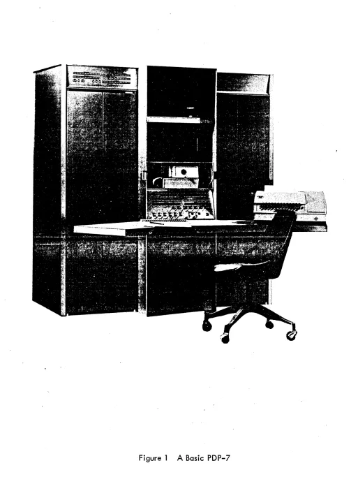
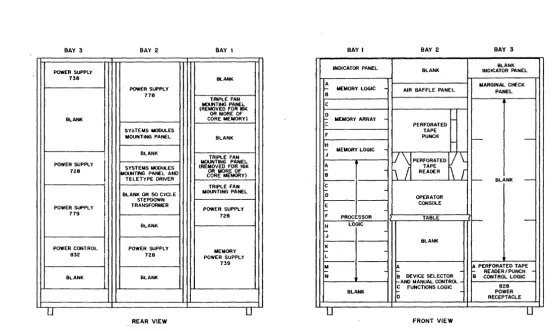
The basic PDP-7 is housed in three metal DEC computer cabinets bolted together to form an integrated console. Double doors at the front allow access to the wiring side of all module-mounting pa~els. Double rear doors pj'ovide access to a plenum door on which the power sup-plies are mounted. Opening the plenum,door yields access to the modules. Logical component locations are shown on Figure 2and dimensions are indicated on Figure 3. For additional physi-cal data refer to the PDP-7 Installation Manual F-780r the PDP-7 Maintenance Manual F-77.
BAY 3
POWER SUPPLY 738
BLANK
I
POWER SUPPLY 728
I
POWER SUPPLY 779
POWER CONTROL 832
BLANK
U
BAY 2 BAY I
BLANK POWER SUPPLY
778
TRIPLE FAN MOUNTING PANEL (REMOVED FOR 161(
OR MORE OF CORE MEMORY)
SYSTEMS NOOULES
MOUNTING PANEL BLANK
BLANK
TRIPLE FAN MOUNTING PANEL SYSTEMS MOOI.lL.ES (REMOVED FOR 16K MOl.WTWG PANEL AND CORE MEMORY) OR MORE OF
TELETYPE DRIVER
TRIPLE FAN BLANK OR 50 CYCLE MOUNTING PANEL
STEPOOWN TRANSFORMER
POWER SUPPLY 728
BLANK
POWER SUPPLY MEMORY 728 POWER SUPPLY
739
BLANK
U
REAR VIEW
BAY I
INDICATOR PANEL
A
r MEMORY LOGIC
-B
C
D
~ MEMORY ARRAY
-H
- MEMORY LOGIC
-J
BAY 2
BLANK
AIR BAFFLE PANEL
I-1/
\J
PERFORATEDV \.
BAY 3
BLANK INDICATOR PANEL
MARGINAL CHECK PANEL
--i
-
i\
11
Rl::iR~
r
~---I---~
--
BLANK-C -D E
-OPERATOR CONSOLEF PROCESSOR TABLE
rH----~L~O~~C~~--~~~----~~~---.~~--I~---~~~----~~I
--J K r L M l-Nu
-BLANK BLANK ~B DEVICE SELECTOR f AND MANUAL CONTROL
-C FUNCTIONS LOGIC
f-
-D
FRONT VIEW
,
IA PERFORATED TAPE f- READER/PUNCH B CONTROL LOGIC
828 POWER RECEPTACLE
u
[image:17.798.113.665.132.463.2]~--_y-~--~~~--+---+---6It·---T----~
+ +
+
+
+
+~---
68~'---FLOOR PLAN
SWINGING DOORS (tol
LOAD POINT
REMOVEABLE END PANEL
SCREEN (TYPICAL
FOR 3 CABlNETSI
69-r
ic=7C=
27fs .
Figure 3 Basic PDP-7 Installation Dimensions
33-h.·~
/
... - - - 27
tk· ---/
!
\'"'.1 ~
[image:18.792.73.701.71.511.2]COMPUTER ORGANIZATION
The PDP-7 system is organized into a processor, core memory, interface, and input/output e~uipment and 'facil ities as shown in Figure 4. All arithmetic, logic, and system control opera-tions of the standard PD P-7 are performed by the processor. Permanent (longer than one instruc-ticn time) local information storage and retrieval operations are performed by the core memory. The memory is continuousl y cye! ing, automatically performing a read and write operation during each computer cycle. Input and output address and data buffering for the core memory is per~ formed by registers of the processor, and operation of the memory is under control of timing signals produced by the processor.
Figure 4 Computer System Block Diagram
Interface circuits allow connections to a variety of peripheral equipment, are responsible for detecting all I/O select codes, and for providing any necessary input or output gating. Indi-vidually programmed data transfers between the processor' and peripheral equipment take place through the processor accumulator. Single or multiple data transfers can be initiated by peri-pheral equipment rather than by the program, by means of the .data break facil ities. Standard features of the PDP-7 also allow peripheral equipment to perform certain control functions such . as instruction skipping, and transfer of program control initiated by a program interrupt.
Processor
The processor performs logical and arithmetic functions, provides access to and from memory and controls the flow of data to. and from the computer. It consists of the processor control, and six active major registers.
Accumu I ator(AC)
Link (L)
This l-bit register extends the arithmetic facility of the accumulator and greatly simplifies programming of arithmetic operations.
Memory Address Register (MA)
This l3-bit register holds the address of the core memory location currently being used.
Memory Buffer Register (MB)
This l8-bit register serves as a buffer for all information sent to or received from core memory.
Instruction Register (lR)
This 4-bit register holds the operation code of the program instruction currently being performed.
Program Counter (PC)
This l3-bit regi~ter holds the address of the next memory location from which an instruction is to be taken.
Core Memory
The high-speed random-access core memory is a 4096-word coincident-current core module with a cycle time of 1 .75 microseconds. In one cycle the memory control retrieves an la-bit word stored in the memory location specified by the memory address register, writes the word by a parallel transfer into the memory buffer register, and rewrites the word into the same memory address.
Interface
The interface control I inks the processor to 64 input and output stations, cal Is the stations, and collects and distributes the input/output data. It also controls the interleaving of data during a data break (cycle stealing), senses the status of I/O devices and skips instructions based on this status, traps lOT ·(input/output transfer) instructions initiating a program interrupt break, and generates real time signal pulses for use by external peripheral equipment.
Input/ Output
Standard input/output equipment provided with each PDP-7 consists of a Teleprinter and Con-trol Type 649, Perforated Tape Reader and ConCon-trol Type 444B, and a Perforated Tape Punch and Control Type 75D.
Teleprinter and Control Type 649
A Teletype Model 33 Keyboard Send Receive (KSR) set and an appropriate DEC control con-stitute this equipment. The Teletype unit is a standard machine operating from serial ll-unit-code characters at a rate of ten characters per second. The Teletype provides a means of sup-plying data to the computer by means of a keyboard and suppl ies data as an output from the computer in the form of typed copy. The Teletype control serves as a serial-to-parallel con-verter for Teletype inputs to the computer and serves as a parallel-to-serial concon-verter for com-puter output signals to the Teletype unit It
Perforated Tape Reader and Control Type 444B
This equipment senses eight-channel, fan-fold perforated Mylar or paper tape photoelectrically at 300 characters per second. The reader is a Digitronics 2500 and the control is a DEC data register, flag, and associated logic circuits.
Perforated Tape Punch and Control Type 75D
This equipment consists of a control unit and a Teletype BRPE punch that perforates eight-channel, fan-fold paper tape at 63.3 lines per second.
Processor Options
Extended Arithmetic Element Type 177
Automatic Priority Interrupt Type 172
The Automatic Priority Interrupt increases the capacity of the PDP-7 to hand I e transfers of in-formation to and from input/output devices by identifying an interrupting device directly, without the need for flag searching. Multilevel program interrupts are permissible where a device of higher priority supersedes an interrupt already in process. These functions increase the speed of the input/output system and simplify the programming. More and faster devices can therefore be serviced efficiently.
The Type 172 contains 16 automatic interrupt channels arranged in a priority sequence so that channel
°
has the highest priority and channel 178 has the lowest priority. The pri()rity chain guarantees that if two or more I/O devices request an interrupt concurrently, the system grants the interrupt to the device with the highest priority. The other interrupts will be serviced afterwards in priority order.Data Interrupt Multiplexer Type 173
The single PDP-7 data break interrupt channel is expanded to handle information transfers with three high-speed I/O devices by addition of the Type 173 option. This option provides multi-plex control for simultaneous operation of three high-speed devices such as magnetic tape or drum devices. Maximum combined transfer rate is 570,000 l8-bit words per second.
Memory Jncrement Type 197
This option allows an external condition or signal from an I/O device to increment the content of any core memory location. The peripheral device initiates a break cycle so that the content of a core memory address specified by the device is read into the memory buffer register, in-cremented by one, and written back into the some address in one computer cycle.
~oundary Register and Control Type KA70A
This option establishes core memory address boundaries that can be assigned to speciific users when the system is used for real time computing with simul taneous multiuser program execution.
Core Memory Options
~emory Extension Control Type 148
Core Memory Module Type 147
Th is option extends the capac ity of the standard 4096-word memory to 8192 words.
Core Memory Modul e Type 1498
This option extends the capacity of the PDP-7 core memory by one field of 8192 words. The 1498 option can be added only to memories of 8K, 16K, or 24K capacity (not to 4K, 12K, etc. without also adding a Type 147 module).
Memory Parity Type 176
This option assures rei iabil ity of all core memory data storage and retrieval operations by generating, storing, and checking parity on every transfer. An odd parity bit is generated and written in the same core location as the word being written. Upon reading, a word drawn from core memory is checked for parity and if odd parity is detected a program interrupt is initiated or the program is halted.
Input/Output Options
Card Reader and Control Type CR018
Standard 12-row, 80-column punched cards are read by this device in either alphanumeric or binary mode. Reading is accomplished by mechanical sensors at a maximum rate of 100 cards per minute.
Card Reader and Control Type 421
Standard punched cards are read optically at up to 200 cards per minute on the Type 421 A, or up to' 800 cards per minute on the Type 4218. Information punched on the cards is read col umn by column in binary or alphanumeric modes.
Card Punch Control Type 40
Automatic Line Printer and Control Type 647
This machine prints a selection of 64 characters on a I ine of 120 characters at a rate of 300, 600, or 1000 I ines per minute. Printing is performed by solenoid-actuated print hammers. Load ing, printing, and format are under program control. Format is program sel ected from a punched format tape in the printer ..
DECtape Dual Transport Type 555 and Control Type 550
The DECtape system provides a unique fixed address magnetic-tape facil ity for high··speed loading, readout, and program updating. Each DECtape transport contains two independent tape drives. Up to four transports (eight drives) can be used with one control.
Read, write, and search speed is 80 inches a second. Density is 375 bits an inch. The two logically independent transports have a storage capacity of 3 mill ion bits each.. Phase record-ing, rather than ampl itude recording; redundant, nonadjacent data tracks; and a prerecorded timing and mark track are features of this system. The control searches in either direction for specified block numbers, the~ reads or writes data. Units as small as a single word may be addressed.
Automatic Magnetic Tape Control Type 57 A
Up to eight IBM or IBM-compatible tape transports can be operated automatically by the Type 57 A to transfer information through the PDP-7 data break interrupt fac
iI
ity. Magnetic tape transports are controlled to read or write at densities of 200, 556, or 800 characters per inch at speeds of 75 or 112.5 inches per second. .Magnet i c Tape Transport Type 570
The Type 570 is a highly sophisticated tape transport that reads and writes at 75 or 112.5 inches per second at program-selected densities of 200, 556, or 800 characters per inch. Tape motion is controlled by pneumatic capstans and brakes, el iminating conventional pinch rollers, clamps, and mechanical arms. Tape width is one-half inch, with six data tracks and one parity track. Format is IBM compatible.. Dual heads permit read-checking while writing. The TYlPe 570 contains a multiplex interface which permits time-shared use of the transport by two Type 57A tape control on the same or different computers~
Magnetic Tape Transport Type 545
Magnet i c Tape Transport Type 50
The Type 50 can be used with the Type_oS7 A to read or write IBM-compatible magnetic tapes at transfer rates of 15,000 or 41,700 characters per second. Tape speed is 75 inches per second at densities of 200 or 556 characters per inch.
Block Transfer Serial Drum System Type 24
Drum transfers operate through the computer data interrupt facil ity permitting interlaced pro-gram and drum transfer operation. Stvrage capacities of 32,768 words, 65,536 words, or 131,072 words are availabl e.
Incremental Plotter Control Type 350
One California Computer Products Digital Incremental Recorder can be operated from a DEC Increment Plotter Control Type 350 to provide high-speed plotting of points, continuous curves, points connected by curves, curve identification symbols, letters, and numerals under program control. The recorder can be selected from four models, that differ in speed (12,000 or 18,000 steps per minute), step size (0.01 or 0.005 inches per step), and paper width (12 or 51 inches).
Oscilloscope Display Type 34A
Computer data can be plotted point-by-point on a 5-inch oscilloscope, such as the Tektronix Model RM503, by the option. The horizontal axis of each point is determined by 10 binary bits, and the vertical axis is determined by another 10 binary bits. This option can be obtained with or without the oscilloscope.
Precision CRT Display Type 300
The Type 300 is a random-position point-plotting display with a sel f-contained, 16-inch CRT using magnetic deflection and focusing. Data is plotted point by point in a raster .9-3/8 inches square having 1024 points on a side according to separately variable 10-bit X and Y coordinates. The display includes program intensity control. Plotting rate is 35 microseconds per point.
Symbol Generators Type 33 and Type 342
Precision Incremental CRT Display Type 340
Plots points, I ines, vectors, and characters on a raster identical to the 30. Plott,ing rate is 1-1/2 microseconds per point in vector, increment, and character modes. Random point plotting is 35 microseconds.
Photomultiplier Light Pen Type 370
A fiber optic I ight pipe and photomultipl ier in the I ight pen all ow high-speed detection of information displayed on the Type 34A, 30D, or 340 displays. Detection of information by rne Type 370 can be sampled by the computer to alter the program.
General Purpose Analog-to-Digital Converter Type 138E
The Type 138E is a high-speed successive approximation converter with analog input signal range from 0 to 10 volts. The analog voltage is converted to a binary number, selectable from 6 to 12 bits. Conversion time varies, depending on the number of bits and the accuracy required. Combinations of switching point accuracy and number of bits can be selected on a front panel switch.
High Speed Ana
I
og-to- Dig itaI
Converter Type 142Transforms an analog voltage to a single, 10-bit binary number in 6 microseconds. Conversion accuracy is ±0.15% ±1/2 least significant bit.
General Purpose Multiplexer and Control Type 139E
Up to 64 analog input channels can be selected for application to the input of the Type 142 or Type 138E by the Type 139E. Channels can be program selected in sequence or by individual address. The number of channels that can be selected is determined by the number of optional Multiplexer Switches Type Al00 series used in the Type 139E. Each Type A100 can select two channels.
Analog-Digital-Analog Converter System Type ADA-1
Performs fast, real-time conversion between digital and analog computers. MaximlJm sample rate for
0/
A conversion is 200 kc; for A/D and interlaced conversions, 100 kc. Digital word length is 10 bits. Actual conversion times are 5 microseconds for A/D and 2 microseconds forData Control Type 174
The Data Control Type 174 controls and buffers the transfer of data blocks between the PDP-7 and up to three external devices. Block transfers are made from consecutive memory locations to one device at a time. The data control counts the number of data words transferred, buffers either incoming or outgoing information until the transfer is complete and signals the comple-tion of a transfer .. Maximum data transfer rate is 1.75 microseconds per lS-bit word, or 570,000 lS-bit words per second.
Data Communication Systems Type 630
This system is a real-time interface between Teletype stations and the PDP-7 and is ideal for multi-user computer time-sharing message switching systems, and data collection-processing systems. A variety of Type 630 systems are available for half-duplex and full-duplex opera-tion with up to 64 staopera-tions.
Relay Output Buffer Type 140
A data buffer register loaded from the computer accumulator actuates lS relays, each having mercury-wetted single-pole double throw contacts. These contacts can be used for direct digital control or signal generation for external equipment.
Int'er Processor Buffer Type 195
This device serves as an interface between a PDP-7 and another computer to permit bi-directional data communication with an asynchronous processor.
PROGRAMMING SYSTEM
The PDP-7 Programming System includes an advanced FORTRAN compiler, a symbolic assembler, symbol ic tape editor, Digital debugging system (DDT), maintenance routi~es and a I ibrary of arithmetic, util ity and programming aids developed on the program-compatible PDP-4. Both the symbol ic tape editor and DDT are designed to a II ow symbol ic debugging and computer-aided editing to replace the tedious manual equivalent. New and, updated programs are beIng developed continuously in the appl ied programming department.
FORTRAN Compil er
knowledge of computer organization and machine language to write effective programs. Programs are written in a language of famil iar Engl ish words and mathematical symbols. Com-pilation of the original FORTRAN source program is performed separately from the comCom-pilation o'F associated subroutines. Thus, when errors in FORTRAN coding are detected by the compiler diagnostic, only the erroneous program need be recompil ed.
Symbolic Assembler
The symbolic assembler allows the programmer to code instructions in a symbolic language. The assembler USbJ on the PDP-7 allows mnemonic symbols to be used for instruction codes and
addresses. Constant and variable storage registers can be automatically assigned. This assem-bler produces a binary object tape and I ists a symbol table with memory allocations and useful diagnostic messages.
Digital Debugging Tape (DDT)
DDT speeds program debugging by communicating with the user in the address symbols of the source language program. Program debugging time is further shortened when using DDT because program execution and modification are controlled from the teleprinter keyboard. For exampl e, to branch to a new location in the program it is only necessary to type the symbol ic location name on the keyboard, followed by the single quote (I) character. The same symbol followed by the slash
V)
character, causes the content of that location to be typed. By using DDT to insert break points in a program, the programmer can make corrections or insert patches and try them out immediately. Working corrections can be punched on tape immediately in the fc)rm of loadable patch tapes, el iminating the necessity of creating new symbol ic tapes and reassembl ing each time an error is found.Symbol ic Tape Editor
The editor program permits the editing of source language programs by adding or deleting lines of text. All modification, reading, punching, etc., is controlled by symbols typed at the key-board. The editor reads parts or all of a symbol ic tape into memory where it is available for
immediate examination, correction, and rei isting.
Bus-Pak II
SYMBOLS
The following special symbols are used throughout this handbook to explain the function of equipment and instructions:
Symbol
A =
>
BO=>A
Ai
A5A5(l)
A6 - 11
A6 - 11
=
>
BO - 5Y
V
~-/\
A
+l=>A
Explanation
- The content of register A is transferred into register B
Register A is cleared to contain all binary zeros
Any giver" bit in A
The content of bit 5 of register A
Bit 5 of register A contains a 1
The content of bits 6 through 11 of register A
The content of bits 6 through 11 of register A is transferred into bits 0 through 5 of register B
The content of any core memory location
Inclusive OR
Exclusive OR
AND
One's complement of the content of A
SECTION 2
FUNCTIONAL DESCRIPTION
The standard PDP-7, as mentioned in Section 1, can be analyzed into a process.or, a core memory, interface elements, and input/output equipment.
PROCESSOR
Te> perform logical, arithmetic, data processing, and control functions the processor employs
seven active registers. Intel I igence flow among these registers and between them and other
major elements of the computer system is shown on Figure 5.
, - - - ,
1 - - 1
ADDRESS I
I
oo~~n~roIN~vOO~~---~-~---~----~
I
IEQUIPMENT USING THE DATA _DA_TA _ _ _ _ _ _ ---,r-+I _ _ _ _ ---, MEMORY I ADDRESS
I
BREAK ...- ~ t~81~~~SR
1--
;'~ggi
I
i
UN',~~3~;:~"
i i i
.... DATA ..
I _ _ _ _
~
I
MEMORYI+----L--_,--'~
I
II
CONNECTION TO STANDARD ... ".. ACCUMULATOR:'-- BUFFER 1 - - - 'AND OPTIONAL INPUT I OUTPUT
I .
I REGISTER I DATA I 1EQUIPMENT USING PROGRAMMED CONTROL
I
I ----JII1DATA TRANSFERS 4 .. ·
I
1 18 lB ~ II
I
I
G'~~~~O.
_
'~~'ii~~i~ON
i
i
:
I
I
I
4 4I
I
I
~~E --.J ~O~R _ _ _ _ _ _ _ _ _ _ _ _ _ --.J
Figure 5 Major Register Block Diagram of the Processor
Accumu lator (AC)
Link (L)
This one-bit register is used to extend the arithmetic capabil ity of the accumulator. In l's complement arithmetic, the link is an overflow indicator; in 21
s complement it logically extends the AC to 19 bits and functions as a carry register. Overflow into the I ink from the accumulator can be checked by the program to greatly simplify and speed up single and multiple precision arithmetic routines. The link can be cleared and complemented and its state sensed independent of the AC. It is included with the AC in rotate operations.
Memory Address Register (MA)
The address of the core memory cell currently being accessed is contained in the 13-bit MA. Information enters the MA from the memory buffer register program counter, or from external device operating in a data interrupt. Addition of the Memory Extension Control Type 148 option expands the MA to 15 bits.
Program Counter (PC)
The program sequence, that is the order in which instructions are performed, is determined by the PC. This 13-bit register contains the address of the memory cell from which the next instruction is to be taken. Information enters the PC from the MA, MB, or the ADDRESS switches of the operator console. Addition of the Memory Extension Control Type 148 option expends the PC to 15 bits.
Memory Buffer Register (MB)
All information transferred into or out of core memory passes through the MB. Information is read from a memory cell into the MB and rewritten into the cell in one cycle time (1.75 /Jsec).
Instructions and data are brought from core memory into the MB for processing. The MB serves also as a buffer for information transferred between core memory and an external device in a data interrupt. The content of the MB may be incremented by one.
Instruction Register (lR)
Ma jor State Generator
The computer operates in one of four major control states during each machine timing cycle. One or more states are entered to execute an instruction. The states are Fetch, Execute, Defer, and Break and are determined by the major state generator. Only one state exists at a "time and all states, except Break, are determined by the programmed instruction being executed.
Fetch (F)
A new instruction is obtained when this state is entered. The content of the memory cell specified by the PC is placed in the MB, and the operation code (bits 0-3) of this instruction word are placed in the IR. The content of the PC is then incremented by one. If CJ single-cycle instruction is fetch,ed, the operations specified are performed during the last part of the fetch cycle, then the nexf:state is fetch for the next instruction. If a two-cycle instruction is fetched, the succeeding control state is either defer or execute.
Defer (D)
When bit 4 of a memory reference instruction is a
1,
the defer state is entered to perform the indirect addressing. The memory location addressed by the instruction contains the address of the operand, and access to the operand is deferred to the next memory cycle.Execute (E)
This state is established only when a memory reference instruction is being executed. The content of the memory cell addressed is brought into the MB, and the operation spE~cified
by the content of the IR is performed.
~'eak (B)
Detail ed Processor Block Diagram Discussion
All logic circuit elements of the processor are shown on Fi gure 6. These el ements consist of controls for the major registers, the essential timing generator for the computer system, the manual controls, and the special program feature controls (program interrupt, data break interrupt, I/O skip, I/O trap, etc.).
FROM INPUT/ouTPUT EQUI PMENT USING DATA BREAK TRANSFERS
FROM INPUT/OUTPUT EQUIPMENT uSING PROGRAMMED STATUS CHECKS
TO DEVICE SELECTOR OF INTERFACE
FROM INPUT/OUTPuT EQUIPMENT VIA THE INFORMATION COLLECTOR OF THE INTERFACE
TO INPUT/OUTPUT EQUIPMENT VIA THE INFORMATION DISTRIBUTOR OF THE INTERFACE
FOR INPUT/OUTPUT EQUIPMENT USING DATA BREAK TRANSFERS
DIRECT CONNECTION AVAILABLE FOR ANY INPUT /OUTPUT EQUIPMENT OR FOR DEVICE SELECTOR OF INTERFACE
DIRECT CONNECTION AVAILABLE FOR ANY INPUT/OUTPUT EQUIPMENT
ADDRESS
MEMORY BUFFER REGISTER
PROGRAM COUNTER
15
MA CONTROL
MEMORY ADDRESS REGISTER
'15
AuDRESS TO CORE ... MEMORY
~ ______ - , _____________________ D_A_T_A __ ~~g:~~~~O~y
INCREMENT MB
CLEAR AC
MINOR STATES (INSTRUCTION STATES)
MAJOR STATES (F,O,E,B)
1
ADDRESS ACCEPTED
DATA ACCEPTED
r
PROGRAM INTERRUPT REQUEST
POWER CLEAR PULSE
SPECIAL PULSES {SPO, 1,2,3,4)
TIMING PULSES (TI THROUGH T7)
REQUEST SLOW CYCLE
MB CONTROL
18
PROGRAM INTERRUPT
SYNC,
BREAK REQUEST
Figure 6 Detailed Block Diagram of the Processor
[image:33.620.69.549.166.704.2]Timing Generators
The power clear pulse generator produces pulses to clear processor and I/O device register when the computer is energized or de-energized. Spec ia I pu Ises produced to enact computer function initiated by manual controls are also available for use by peripheral equipment. The timing signal generator produces the basic timing pulses that control all processor operations. The timing of these pulses can be in a normal fast cycle or in a slow cycle requested by a
signal from an I/O device. The slow cycle is used to exes:;ute input/output transfer instructions that communicate with equipment that is not fast enough to act upon rapid successive command pulses.
Manual Controls
Control keys and switches allow the normal start/stop/continue control, control special single-cycle and single-instruction operation for maintenance of the machine, control the use of the special program features, and provide a means of loading data directly into the computer. The switch register is used to store an la-bit word in the AC and the ADDRESS switch register is used to load a 15-bit core memory address into the PC. Use of the manual controls provides rapid entry of program information on perforated tapes and a broad means of modifying programs
or data in core memory. '
Input/Output Skip
This facility allows the program to skip or not skip the next instruction according to the con-dition of an external device flag. Skipping is accompl ished by incrementing the content of the PC so that execution of an instruction is by-passed. This facility simplifies program branching or decision-making based upon the condition of device status lines.
Input/Output Trap
Basic hardware that allows the PDP-7 to serve in time-sharing applications is provided as the I/O trap facility. These circuits monitor instructions being performed and initiate a program interrupt if an instruction is encountered that will interfere with the execution of other pro-grams. The interrupt program can then determine the cause of the trap and take appropriate action. The I/O trap feature can be enabled or disabled by a switch ori theoperator console or by programmed instruct ion.
Program Interrupt Control and Synchronization
the content of the I ink, the condition of the memory extend mode control, the condition of the I/O trap, the content of the extend PC, and the content of the PC in core memory loca-tion
O.
Memory location 1 is then placed in the PC to transfer program control to the sub-routine. Upon conclusion of the subroutine, the initial program is returned to its previous state by using the information stored in locationO.
Data Break Interrupt
Peripheral equipment can cause temporary suspension of the main program to "steal" a cycle of computer time for the transfer of information with core memory. A data break request re-ceived by the program interrupt synchronization element is honored at the end of execution of the current instructior.. The Break state is then entered and control
I
ed by the peripheral device. The device specifies a core memory address at which the transfer is to occur, and designates the direction of the transfer as into or out of core memory. The address is suppl ied to the MA and the data transfer is enacted between the device and the MB. At compl etion of the Break cycle the interrupted program is continued, unl ess the device has requested an-other data break. One I/O device can be connected to cause data breaks, or up to four de-vices can be connected through the Data Interrupt Multiplexer Control Type 173.Real Time Clock
A clock within the standard computer causes a clock data break interrupt (in the same manner as described previously for an external device data break) every 1/60 second, so that program events can be related to real time. When this interrupt occurs the content of core memory loca-tion 7 is incremented by 1 during the Break cycl e and serves as a counter. Any number can be stored in address
7
so that it overflows (counts up to zero) at a time multiple of 1/60 second and this stored number. When overflow, occurs the clock flag is set and initiates a program interrupt.CORE MEMORY
The core memory provides storage for instructions to be performed and information to be pro-cessed or distributed. This random-address ferrite-core memory holds 4096 18-bit words in the standard PDP-7. Optional equipment extends the storage capacity in blocks of 4096 or fields of 8192 words, or expands the word
I
ength to 19 bits to provide parity check ing. ~Aem ory location 08 is used to store the content of the PC following a program interrupt, and loca-tion 18 is used to store the first instrucloca-tion to be executed following a program interrupt;.(When a program interrupt occurs, the content of the PC is stored in location 08' and program control is transferred to location 1 automatically.) Location 78 is used with the real time clock and locations 108 through 178 are used for auto-indexing. Location 20 is used to store information during a call subroutine (CAL) instruction and location 20 is used as the starting address of the CAL handl ing subroutine. All other locations can be used to store instructions or data.
the electrical conversions necessary to transfer information into or out of the core array and perform no arithmetic or logic operations upon the data. Since their operation is not discernible by the programmer or operator of the PDP-7, these circuits are not described her~ in detail.
FROM MEMORY ADDRESS REGISTER OF PROCESSOR
FROM MEMORY BUFFER REGISTER OF PROCESSOR
ADDRESS (MA 0-'5)
DATA (M8 0-'8)
SELECT
MEMORY READ SELECTOR
~~~MT:"~:::U~~~AR TIMING PULSES MEMORY CONTROl. GENERATORS OF
PROCESSOR
TO MEMORY BUFFER
~~~:~~~IO~N~EGISTER +=D;:.AT:.::A....!(~SA;:..:0:...-.:.:'8.:...)
---1
A~~~F~~RS ~---'OF PROCESSOR
MASTER SI.ICE CONTROL
Figure 7 Core Memory Block Diagram
INTERFACE
Information is transferred to peripheral equipment from the processor by means of an information distributor. Information is transferred to the processor from I/O devices by the information collector. Addressing of a device to receive programmed command signals is accomplished by means of the device selector. These three logic circuit elements constitute the major PDP-7 data interface and are shown in Figure 8. Control interface is effected by elements of the processor, as described previously in this section. Timing of the processor as related to
interface and input/output operations is shown on Figure 9.
TO SELECTED INPUT IOUTPUT I/OT PULSES I/OP 1,2,4 FROM lOP PULSE GENERATOR OF
EQUIPMENT PROCESSOR
TO ALL INPUT 10UTPUT AC DATA AC DATA OUT FROM ACCUMULATOR
EQUIPMENT OF PROCESSOR
FROM ALl. INPUT/OUTPUT AC DATA AC DATA IN TO ACCUMULATOR
EQUIPMENT OF PROCESSOR
[image:36.613.70.516.133.339.2]COMPUTER TIMt IN NANOSECONDS
TIMING PULSE GENERATOR
COMPOSIT OUTPUT GROLfID : 150"":
! NSEC ! :"'240 . .l
: NSEC :
t l
T6 T7
I I
: - ANY I10T(I~~~T~=C~SC:·j) CYCLE _ _ _ _ _ !
~ f---N~----': N~fc:' ~ :1:"~iE~-,: ~ r-~C :-N~~-1
: : i ! ~ : 6 7 0 _i :
... ..- 90 _ 270.... :"'210~ lSO-l ~ _ _ _
i
i
NSECi
NSECi
INSEC: NSEC::!
NSEC!
:
TI T2 T3 T4 T5 T6 T7 TI T2 T3 T4I I I I I I I I I I I
---: l-N~C
I I
I I
:.... 120 I
: NSEC:
~ T~ I I
(40 NSEC PULSES) -3 \tOLlS - T6 T7 TI T2 T3 T4 T5 T6 T7 TI T2 T3 T4 T5 T6
MEMORY BUFFER REGISTER OUTPUT
NOTAVA~---,
r-*
AVAlI..ABI..E _ L -_ _ _ _ _ _ _ _ _ _ _ ~
ACCUMULATOR DATA FOR OUTPUT TRANSFER
NOr REAIY( - : / ~_ r~ ______________________________________ T6 TtOO NSEC ~~T4T20NSEC
~~~rm~~~~DFOR NOT~---;;4--,L---~ IF MB 14 CONTAINS A I ~ - T4 T 100 NSEC
r-TI OF NEXT CYCLE T 20 NSEC IIOP PULSE GENERATOR COMPOSIT Gf/()(JM) T5T20 NSEC...I I
/LJ"l.r
OUTPUT (70 NSEC PULSES) -3\tOLTS - I1C»>IT7.20 NSEC lIOP2 I/OP4
, ri r f TI OF NEXT CYCLE T40 NSEC
~~~\ r~~~1~ pu~~IT
_=
- _ - - - T - 5 + - 4 - 0 - N S E - C - : : u ' T7-t40NSEC"'"'LJ UCOMPUTER TIME IN NANOSECONDS TIMING PULSE GENERATOR COMPOStT OUTPUT (40 NSEC PULSES)
GROUND 150 I
NSEC--':
I
;'-~-l 16 n
I I
I/OT XXOI lIOT XX02 lIOT XX04
(a) NORMAL CYCLE
r--. 90 120 •
-: r-NSEC . NSECi
: !--~C----+~C--l
TI T2 T3 T4
i I I I
-3 \tOLlS - 16
n TI 12 T3 T4 T5 T6 T7 Tl12
MEMORY BUFFER NOT AVAILABLE - - - , .---~IJ
REGISTER OUTPUT AVA/LASLO: _ L -_ _ _ _ _ _ _ _ _ _ _ _ _ _ _ _ _ _ _ _ _ _ _ _ _ _ _ _ _ _ _ ..J
T4 T5 T6
ACCUMULATOR DATA FOR NOTREADY - y T6+tOONSEC F=i"4+20NSEC
OUTPUT TRANSFER REAIY(- L _ _ _ _ _ _ _ _ _ _ _ _ _ _ _ _ _ _ _ _ _ _ _ _ _ _ _ _ _ _ _ _ _ _ _ _ _ _ _ _ _ _ _ _ _ _ _ _ _ _ _ _ _ _ _ _ _ _ _ _ ~.
ACCUMULATOR CLEARED FOR NOT REAIY( - - - -_ _ - ,
Pt1\:~~~:f.:'1RI R£A(J'( - T4 + 100 N S E C ; : : : I ' - - - ' 110 PULSE GENERATOR COMPOSET GROUND ---::::u-,
OUTPUT (70 NSEC PULSES) -3 VOLTS - T5 +20 NSEC I/OP I DEVICE SELECTOR COMPOSITE
OUTPUT (400 NSEC PULSES)
GROUND - - - ,
-3 VOLTS - T5+40 NSEC--iL-::-:-:c:::-:-::c:-::-..J lIOT XXOI
(bl SLOW CYCLE
T7 + 20 NSEC::::tJ TI OF NEXT CYCLE + 20 NSEC::;ur---,{f
lIOP2 llOP 4
T7+40 NSEC:;J .... --I-:-IO:"::T-X-X-0-2 .... 11 OF NEXT ;;J