SIGNAL GENERATOR BASED ON THE VIRTUAL
INSTRUMENT TECHNOLOGY
YAN LIU,YINGYING SHENG, MANQIONG TAN
College of Information Science and Engineering, Hunan University, Changsha 410082, China
ABSTRACT
A high-precision and stable signal generator with extremely low frequency is the ideal equipment in machinery, civil engineering, communication and vibration test. To meet the demands of these special areas, the paper designs such a signal generator based on virtual instrument using hybrid system with MCU and FPGA. The system consists of a host and a slave computer. The slave computer uses a MCU via the DDS technology to make FPGA generate periodic signal with adjustable frequency. The virtual instrument technology is introduced into the host computer (PC), which uses LabVIEW to set the signal parameters and realize the GUI system. The results of our implementation show that the signal generator can generate frequency varying from 0.01Hz to 20 kHz, including sine wave, square wave and triangle wave. It has been successfully used in the vibration measure of some engineering areas.
Keywords: Signal Generator, DDS, FPGA, Virtual Instrument 1. INTRODUCTION
The development of electronic, semiconductor and computer technology has a deep influence on the development of many other industries and makes many premeditations possible. Signal generator that generates high-precision and stable digital signals is always the important equipment doing related test in lots of fields, such as machinery, civil engineering, communication. Generally, most signal generators used in above industries are achieved by analogue technique and have simple functions, poor stability and poor frequency-division. The digital DDS (Direct Digital Synthesizer) technology has become the major component of signal sources' development. DDS technology is adopted to design a small and convenient signal generator which is digital, high-precision and stable. Flexible MCU and FPGA with strong digital signal processing ability are used to achieve this design and LabVIEW based on virtual instrument technology is used to design a signal source control panel with good man-machine interface. Then users can get conveniently waves of any wanted frequency and amplitude, generated and outputted by the slave computer.
2. RELATED WORK
Based on combination of FPGA and MCU, Liu, et al. [2] design a wave generator that can generate sine, saw-tooth, triangular waves and four PWM waves. For PWM waves, the duty ratio is adjustable from 0 to 100 percent, for others, the frequency is
adjustable from 10Hz to 20KHz. Design of dual DDS generator based on FPGA can generate stable, high-precision, high bandwidth and low attenuation arbitrary waves[5]. A method presented by Sun, et al. [6] generates Costas FH radar signal from the signal set produced by DDS using so-called "frequency-selecting matrix". Their researches have laid a good foundation, but without taking the consideration of that LabVIEW technology performs better in producing all sorts of waveform quickly and easily. LabVIEW technology will shorten the system exploiting time and improve programming efficiency in data collection, testing and survey [1, 7]. This paper extends previous work by using a hybrid system with MCU and FPGA. The MCU controls FPGA to generate periodic signal with adjustable frequency and the least step frequency 0.01Hz, and PC uses LabVIEW to realize the GUI system.
3. DDS WORKING PRINCIPLE
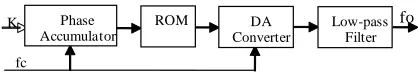
DDS technology based on the concept of phase and sampling principle generates a desired wave by table look-up method. Figure 1 shows the structure of DDS, consisting of phase accumulator, waveform memories ROM, digital to analog converter DA and low pass filter LPF.
fo
K Phase
Accumulator
ROM DA
Converter
Low-pass Filter
[image:1.612.314.523.650.690.2]fc
Phase accumulator consists of bit adder and N-bit accumulator, when a clock pulse fc arrives, adder calculates the sum of frequency control word K and accumulative phase output of accumulator and sends the result to the input of accumulator. Accumulator sends the new phase generated by adder in the previous clock pulse back to the input of adder, so the adder gets the sum continuously of phase and K in the next clock pulse. Phase accumulator controls the linear accumulation constantly of frequency control word K. Phase accumulator accumulates K per clock pulse, thus its output is the phase of mixed signal and its overflow frequency is the output signal frequency of DDS. By the means of phase accumulator's output being used as wave memories' address, the waves stored in the waves memories are encoded(binary coding) to analog, i.e. low pass filter eliminates unnecessary sampling component.
Because f =w/ 2π = ∆θ/ (2π⋅ ∆t) , and ∆θ is the phase increment in a sampling interval∆t, and sampling cycle Δt=1/fc, i.e. f = ∆ ⋅θ fc/ 2π . So
different frequencies can be generated by control
θ
∆ , which is controlled by frequency control word K,∆ = ⋅θ K 2 / 2π N. And K can be changed to get different frequencies fo:
0 ( ) / 2
N c
f = f ×K (1)
From Eq. (1), we know that frequency control word K is proportional to the frequency of the output signal. When the bit width N and clock frequency fc are confirmed, with the increase of K, the times looking up ROM table in a cycle decreases, as well as the time generating a cycle wave, on the contrary, the frequency of output signal increases. And this is DDS technology.
When K=1, the output frequency:
min / 2
N c
f = f (2)
This is the lowest frequency of output signal, also called frequency resolution of signal. Nyquist criterion allows the highest output frequency be
c
f /2, but in fact with LPF constraint, generally:
max
f ≈ fc/4 (3)
In this system, clock source fc =12MHz, accumulator's bit width N=32, from Eq. (2) the frequency resolution of the system can be generated:
6 32
min / 2 12 10 / 2 0.00279 Hz
N
f = fc = × = From
Eq. (3), we know that the highest clock frequency
can be 3MHz.But with stray effects of DDS and post-level analog circuit performance limitations, the ideal range of output frequency is smaller than theoretical frequency, but it can totally meet the low frequency(1.01Hz~20KHz) requirements of mechanical vibration testing and other fields.
When K=256, the amount of sampling point actually will be 224 and pretty good waveforms can be got. The output frequency is:
6 8 32
/ 2N 12 10 2 / 2 46.875 KHz
c
f = f ×k = × × =
DDS technology provides a superior performance to analog signal source and is much better than traditional frequency synthesis technology in many performance indexes, such as relative bandwidth, frequency switching time, high resolution, phase continuity, quadrature output and integration.
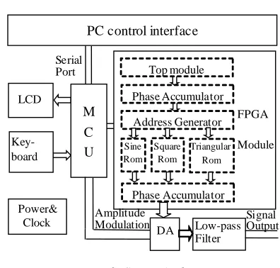
4. SYSTEM DESIGN 4.1. Overall System Design
Serial Port
PC control interface
M C U LCD Key-board Power& Clock Top module Phase Accumulator Address Generator Sine Rom Square Rom Triangular Rom Phase Accumulator FPGA Module Amplitude
Modulation DA Low-pass Filter
[image:2.612.318.516.360.549.2]Signal Output
Figure 2: System Architecture
4.2. Module Design
4.2.1. LabVIEW-based PC software
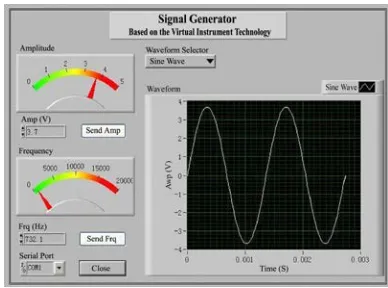
In order to produce all sorts of waveform quickly and easily, the control interface of signal generator is designed by taking advantage of strong data processing capabilities of PC. The interface is as shown in Figure 3.
[image:3.612.315.566.219.370.2]When designing the signal generator interface, we use the control template provided by LabVIEW and place components of simulating the actual signal generator, including data input control, data output control, waveform selector, waveform display control, serial port control and serial port switch. Data input control is used for inputting signal's amplitude and frequency, while data output control for displaying them. Waveform selector is used for selecting signal's waveforms (sine wave, triangular wave or square wave). Once signal's amplitude, frequency and waveform are set, they will be displayed in the waveform display control. Serial port control is used to send signal parameters, set by the user, to the slave computer.
Figure 3: Signal Generator Control Interface
4.2.2. MCU module
MCU as the control center of the system is mainly used to communicate with PC via serial port, scan keyboard, display LCD and control FPGA to finish waveform selection, frequency modulation and amplitude modulation.
MCU program consists of three parts: the timer interrupt service routine, the serial interrupt service routine and the main program. The timer interrupt service routine realizes 5ms timing. The serial interrupt service routine is responsible for receiving the frequency, amplitude, and waveform selection parameters transmitted by PC. The main program consists of two functions: one is to scan keyboard, the other is to check the serial port whether all data
[image:3.612.98.292.380.524.2]has been received. The main program scans the keyboard every 5ms, gets the statistical states of buttons after scanning 20 times(Achieve key debounce by software), gets waveform, frequency and amplitude parameters from these buttons states, sends the encoded parameters to FPGA and displays them. Meanwhile, the main program checks the serial port, if all data has been received, then encodes the parameters to send to FPGA and display them.
Figure 4: Top Design Of DDS
4.2.3. FPGA module
FPGA module is used to realize DDS. The required output frequency range is form 0.01Hz to 20KHz and the least step frequency is 0.01Hz. In term of DDS principle, the least resolution ratio is
N c
f / 2 . To meet the requirements, system clock frequency is set 12MHz, phase accumulator bit width is 32, the largest K is 256 and depth of wavetable is 4096 in consideration of waveform distortion and FPGA storage capacity. Now the output frequency range is from 0.00279Hz to 46.875KHz and the least step frequency is 0.00279Hz.
4.2.4. The latter stage low-pass filter
The filter in this system adopts second-order active filter first and first-order active filter second to eliminate mixed disturbance effectively and adjust the magnification and bandwidth easily. The amplifier of filter uses high-speed low noise OPAMP LF356 whose noise voltage is only 12nV/√z. AS shown in Figure 5.
Figure 5: The Latter Stage Low-Pass Filter
5. SYSTEM TEST
When signal generator design is completed, we begin the system test. In order to uniformly cover the whole testing area, we designed a series of test frequency, form the step frequency 0.01Hz to the maximum frequency 20KHz. Waveform parameters were set through the control interface in Figure 3. Test parameters as following:
1) waveforms: sine waveform, triangular waveform and square waveform
2) frequency range: 0.01Hz~20KHz
3) amplitude resolution: 100mv
In order to avoid the attenuation caused by the frequency band limitation of the instrument itself, we choose a digital oscilloscope with 60MHz frequency band and the matched probes for the observation of waveform generated by FPGA.
Table 1: System Frequency Testing Set
Freq./Hz
Test Freq./Hz
Prop. Error/%
Peak Value/V
0.01 0.01 0 5.0
0.1 0.1 0 5.0
1 1 0 5.1
10 10 0 5.0
100 100 0 5.0
1K 1K 0 5.0
10K 10K 0 5.0
20K 20K 0 5.0
We compared the given frequency and the observations, the results as shown in Table. 1.
From Table. 1, we know that the system has a very high accuracy of frequency and that the waveform and amplitude are quite stable by the oscilloscope observation.
6. CONCLUSION
According to the results, we can conclude that the signal generator based on virtual instrument technology can meet the commands of high-precision and stable low and medium frequency in many fields, like machinery, civil engineering, communication and vibration test. The frequency, amplitude and waveform of output signal can be set through PC control panel and also can be set conveniently and efficiently through keyboard in the case without PC.
ACKNOWLEDGEMENTS
This work was supported by Hunan Provincial Natural Science Foundation of China under Grant 12JJ4057, and Hunan Province Science and Technology Project under Grant 2012SK3186 and by the Fundamental Research Funds for the Central Universities, and by Department of Public Security of Hunan Province Project.
REFERENCES:
[1] Chen, C.-I, “Design of Measurement System Based on Signal Reconstruction for Analysis and Protection of Distributed Generations”, IEEE Transaction on Industrial Electronics, Vol. 60, No. 4, 2013, pp: 1652-1658.
[2] Sanchez, A.-M.; Pignari, S.A.; Regue, J.-R.; Ribo, M. “Device Modeling for Nonstationary Conducted Emissions Based on Frequency- and
Time-DomainMeasurements”, IEEE
Transaction on Electromagnetic Compatibility, Vol. 54, No. 4, 2012, pp: 738-746.
[3] Maoliu Lin; Yichi Zhang, “Covariance-Matrix-Based Uncertainty Analysis for NVNA
Measurements”, IEEE Transaction on
Instrumentation and Measurement, Vol. 61, No. 1, 2012, pp: 93-102.
[image:4.612.93.269.599.706.2]Informatics, IEEE Conference Publishing Services, May 19-20, 2012, pp: 985-987.
[5] DiDio, J; Chonacky, N. “Caveat emptor - what to know before trying to beat a consumer system into a scientific instrument”, Computing in Science & Engineering, Vol. 6, No. 1, 2004, pp: 5-11.
[6] Korolev, K.A.; McCloy, J.S.; Afsar, M.N. “Transmittance measurements on micro- and
nano-sized ferrite powders in millimeter waves”, Proceeding of International Conference on Infrared, Millimeter and Terahertz Waves, IEEE Conference Publishing Services, Oct 2-7, 2011, pp: 1-2.

![Assessment of Physiological Health Status in Relations to Different Anthropometric and Cardio respiratory Measures of Head Supported Load Carrying Male Porters of Sikkim, India [Article Retracted]](data:image/gif;base64,R0lGODlhAQABAIAAAP///wAAACH5BAEAAAAALAAAAAABAAEAAAICRAEAOw==)