EK-DHV11-TM-002
DHV11
EK-DHV11-TM-002
First Edition, September 1983 Second Edition, November 1985
Copyright
©
1983, 1985 by Digital Equipment CorporationAll Rights Reserved
The information in this document is subject to change without notice. Digital Equipment Corporation assumes no responsibility for any errors herein.
Notice: This equipment generates, uses, and may emit radio frequency energy. The equipment has been tested and found to comply with the limits for a Class A computing device pursuant to Part 15 of FCC rules, which are designed to provide reasonable protection against such radio frequency interference when operated in a commercial environment. Operation of this equipment in a residential area may cause interference in which case the user at his own expense may be required to take measures to correct the interference.
Printed in U.S.A
The following are trademarks of Digital Equipment Corporation.
momoDmo™
DEC DECmate DECUS DECwriter DIBOL MASSBUS
PDP P/OS Professional Rainbow RSTS RSX
RT UNIBUS VAX VMS VT
CHAPTER 1 1.1 1.2 1.2.1 1.2.2 1.2.3 1.2.4 1.2.5 1.3 1.3.1 1.3.2 1.3.3 1.3.3.1 1.3.3.2 1.4 1.4.1 1.4.2 1.4.2.1 1.4.2.2 1.4.2.3 1.4.2.4 1.4.2.5 1.5 1.5.1 1.5.2 1.5.3
CONTENTS
INTRODUCTION Page
SCOPE ... 1-1 OVERVIEW ... , 1-1 General Description ... , 1-1 Physical Description ... , 1-2 Versions of DHV11 ... , 1-4 Configurations ... , 1-4 Connections ... 1-6 SPECIFICATION ... 1-6 Environment Conditions ... , 1-6 Electrical Requirements ... , 1-7 Performance ... , 1-7 Data Rates ... , 1-7 Throughput ... , 1-8 INTERFACES ... 1-8 System Bus Interface. . . .. 1-8 Serial Interfaces ... , 1-8 Interface Standards ... , 1-8 Serial Data Format ... , 1-10 Line Receivers ... , 1-11 Line Transmitters . . . .. 1-11 Speed/Distance Considerations ... , 1-11 FUNCTIONAL DESCRIPTION ... 1-12 Control Function ... , 1-12 Q-Bus Interface ... , 1-12 Serial Interfaces ... , 1-12
CHAPTER 2 INSTALLATION
2.1 2.2 2.3 2.3.1 2.3.2 2.3.3 2.3.3.1 2.3.3.2 2.4 2.4.1 2.4.2 2.5 2.6 2.6.1 2.6.2 2.6.3 2.6.4 2.6.5
2.7.2 2.8 2.8.1 2.8.2 2.8.3 CHAPTER 3 3.1 3.2 3.2.1 3.2.2 3.2.2.1 3.2.2.2 3.2.2.3 3.2.2.4 3.2.2.5 3.2.2.6 3.2.2.7 3.2.2.8 3.2.2.9 3.3 3.3.1 3.3.2 3.3.3 3.3.3.1 3.3.3.2 3.3.3.3 3.3.4 3.3.5 3.3.6 3.3.7 3.3.8 3.3.9 3.3.10 3.3.10.2 3.3.10.3 3.3.10.4 3.4 3.4.1 3.4.2 3.4.3 3.4.3.1 3.4.3.2 3.4.3.3 3.4.4 3.4.5 3.4.6 3.4.7
Floating Vectors ... 2-20 INSTALLATION TESTING ... 2-22 Testing in PDP-11 Systems. . . .. 2-22 Testing in MicroVAX I Systems. . . .. 2-23 Testing in MicroVAX II Systems. . . .. 2-24
PROGRAMMING
SCOPE ... 3-1 REGISTERS ... 3-1 Register Access . . . .. 3-1 Register Bit Definitions. . . .. 3-3 Control and Status Register (CSR) . . . .. 3-4 Receive Buffer (RBUF) . . . .. . . .. 3-6 Transmit Character Register (TXCHAR) . . . .. 3-8 Line Parameter Register (LPR) . . . .. 3-8 Line Status Register (STAT) ... 3-11 Line Control Register (LNCTRL) ... 3-12 Transmit Buffer Address Register Number 1 (TBUFFAD1) ... 3-15 Transmit Buffer Address Register Number 2 (TBUFFAD2) ... 3-15 Transmit DMA Buffer Counter (TBUFFCT) ... 3-16 PROGRAMMING FEATURES ... 3-17 Initialization . . . .. 3-17 Configuration . . . .. 3-17 Transmitting. . . ..
3-18---DMA Transfers ... 3-18 Single Character Programmed Transfers ... . . . .. 3-18 Methods of Control. . . .. 3-19 Receiving. . . .. 3-19 Interrupt Control . . . .. 3-19 Auto X-ON and X-OFF ... 3-19 Error Indication. . . .. . . .. 3-21 Modem Control ... 3-21 Maintenance Programming. . . .. 3-22 Diagnostic Codes ... '. 3-22 Self-Test Diagnostic Codes ... 3-22 Interpretation of Self-Test Codes. . . .. 3-22 Skipping Self-Test. . . .. . . .. 3-23 Background Monitor Program (BMP). . . .. 3-24 PROGRAMMING EXAMPLES .. . . .. 3-24 Resetting the DHV11 ... 3-24 Configuration . . . .. 3-25 Transmitting. . . .. 3-26 Single Character Programmed Transfer ... 3-26 DMA Transfer. . . .. 3-27 Aborting a DMA Transfer . . . .. 3-28 Receiving. . . .. 3-28 Auto X-ON and X-OFF. . . .. 3-29 Checking Diagnostic Codes. . . .. 3-30 Modem Control . . . .. 3-31
CHAPTER 4 TECHNICAL DESCRIPTION 4.1 4.2 4.3 4.3.1 4.3.2. 4.4 4.4.1 4.4.2 4.4.2.1 4.4.2.2 4.4.2.3 4.4.3 4.4.4 4.4.5 4.4.6 4.4.7 4.4.8 4.5 4.5.1 4.5.2 4.6 4.6.1 4.6.2 4.6.3 4.6.4 4.6.4.1 4.6.4.2 4.6.4.3 4.6.4.4 4.6.5 4.7 4.7.1 4.7.1.1 4.7.1.2 4.7.1.3 4.7.1.4 4.7.2 4.7.3 4.7.4 4.7.4.1 4.7.4.2 4.7.5 4.7.6 4.8 4.8.1 4.8.1.1 4.8.1.2 4.8.2
CHAPTER 5 MAINTENANCE 5.1 5.2 5.2.1 5.2.2 5.3 5.3.1 5.3.2 5.4 5.4.1 5.4.1.1 5.4.1.2 5.4.1.3 5.4.2 5.5 5.5.1 5.5.2 5.5.3 5.5.3.1 5.5.4 5.5.5 5.6 5.6.1 5.6.1.1 5.6.1.2 5.6.1.3 5.6.2 5.6.2.1 5.6.2.2 5.7 5.7.1 5.7.2 5.7.3 5.8 5.9 5.10
SCOPE ... 5-1 MAINTENANCE STRATEGY ... " ... " 5-1 Preventive Maintenance. . . .. 5-1 Corrective Maintenance ... " 5-1 INTERNAL DIAGNOSTICS ... " 5-2 Self-Test .. . . .. 5-2 Background Monitor Program (BMP) ... 5-2 XXDP+ DIAGNOSTICS ... 5-2 CVDHA?, CVDHB?, and CVDHC? ... , ... " ... 5-2 Functions of CVDHA? ... " 5-3 Functions of CVDHB? ... " 5-3 Functions of CVDHC? ... " 5-3 DECX/ll Exerciser. . . .. 5-3 DIAGNOSTIC SUPERVISOR SUMMARY ... " 5-3 Loading the Supervisor Diagnostic ... " 5-4 Four Steps to Run a Supervisor Diagnostic ... " 5-4 Supervisor Commands ... 5-5 Command Switches ... " 5-6 Control/Escape Characters Supported ... " 5-6 Example Printouts ... " 5-7 CORRECTIVE MAINTENANCE ON MICROVAX I SYSTEMS .... " 5-8 The Macroverify Diagnostic. . . .. 5-8 Setting Up Procedures ... " 5-9 Bootstrapping Procedure ... " 5-9 Macroverify Operation ... " 5-9 DHVII Diagnostic EHXDH... 5-9 Setting Up Procedures ... " 5-10 Bootstrapping Procedures. . . .. 5-10 RUNNING MICROVAX II DIAGNOSTICS ... 5-18 Overview of the MicroVAX II Maintenance System. . . ... 5-18 Running the Customer Version of the Micro V AX II Diagnostic. . . .. 5-19 Running the Maintenance Version of the Micro VAX II Diagnostic .. " 5-19 FIELD REPLACEABLE UNITS (FRUs). . . .. 5-25 TROUBLESHOOTING FLOWCHART ... " 5-25 COMPONENT REPLACEMENT ... " 5-25 APPENDIX A IC DESCRIPTIONS
Al A2 A2.1 A2.2 A2.3 A3 A3.1 A3.2 A4 AS A6 A7
SCOPE ... A-I 8051 MICROPROCESSOR/MICROCOMPUTER ... " A-I 8051 Block Description. . . .. A-I Configuration. . . .. A-2 Read/Write Timing ... " A-4 SC2681 DUAL UART (DUART) ... " A-5 Block Description ... " A-5 Pin-Out Information ... : . . . .. A-7 DC003 INTERRUPT IC ... " A-9 DC004 PROTOCOL IC ... A-13 DC005 BUS TRANSCEIVER IC ... A-17 DCOlO DIRECT MEMORY ACCESS LOGIC ... " A-21
APPENDIX B MODEM CONTROL
B.1 B.2 B.2.1
SCOPE ... B-1 MODEM CONTROL ... B-1 Example of Auto-Answer Modem Control for the PSTN. . . .. B-2 APPENDIX C GLOSSARY OF TERMS
C.1 C.2
SCOPE ... C-1 GLOSSARY. . . .. C-2
APPENDIX D AUTOMATIC FLOW CONTROL
D.1 OVERVIEW ... D-1 D.2 CONTROL OF TRANSMITTED DATA ... D-1 D.3 CONTROL OF RECEIVED DATA ... D-2 D.3.1 Flow Control by the Level of the Received Character FIFO ... D-2 D.3.2 Flow Control by Program Initiation ... D-3 D.3.3 Mixing the Two Types of Received Data Flow Control ... D-4
APPENDIX E INSTALLATION GUIDE FOR THE DHV11 REMOTE DISTRIBUTION PANEL CABINET KIT
E.1 E.2 E.2.1 E.2.2 E.2.3 E.2A E.3 EA EA.1 EA.1.1 EA.1.2 EA.2
Figure No. 1-1 1-2 1-3 1-4 1-5 2-1 2-2 2-3 2-4 2-5 2-6 2-7 2-8 2-9 2-10 3-1 3-2 4-1 4-2 4-3 4-4 4-5 4-6 4-7 4-8 4-9 4-10 4-11 4-12 4-13 4-14 4-15 4-16 4-17 4-18 4-19 4-20 4-21 4-22 5-1 5:..2 A-I A-2 A-3 A-4 A-5 A-6 A-7 A-8
FIGURES
Title Page
M3104 Module. . . .. 1-3 Example of DHV11 Configuration... . . . .. 1-5 DHVII Connections. . . .. . . .. 1-6 Serial Character Format . . . .. 1-10 DHV11 Functional Block. . . .. . . .. 1-11 Location of Switchpacks. . . .. 2-2 Setting the Device Address . . . .. 2-3 Setting the Vector Address. . . .. 2-4 Bus Grant Continuity . . . .. 2-6 DHVll Installation.. . . .. 2-8 H3173-A Layout. . . .. 2-9 H3173-A Circuit Diagram... 2-10 Staggered Loopback Test Connector. . . .. 2-12 Line Loopback Test Connector. . . .. 2-13 Null Modem Cable Connections. . . .. 2-15· Register Coding. . . .. 3-3 Diagnostic/Status Byte. . . .. 3-22 DHV11 Block Diagram ... 4-2 DATI Bus Cycle. . . .. 4-4 DATO or DATOB Bus Cycle. . . .. 4-4 Interrupt Request/Acknowledge Sequence. . . .. 4-5 DMA Request/Grant Sequence. . . .. 4-5 Common RAM - Memory Map ... 4-7 Common RAM Access. . . .. 4-9 Reading from a Register ... . . . .. 4-13 Writing to a Register. . . .. 4-14 Single-Character Transmit ... . . . .. 4-15 DMA Data Transfer ... 4-16 DMA Character Handling ... 4-17 DMNMemory Error Generation . . . .. 4-18 Receiving a Character ... ~ . . . .. 4-19 PROCI I/O Decoding ... 4-21 PROC2 I/O Decoding. . . .. 4-24 Interrupt Logic. . . .. 4-27 RAM Arbitration and Timing. . . .. 4-28 Store Access Timing Cycle. . . .. 4-29 CSR and Register Address Circuits ... 4-32 DHVII Voltage Converter ... 4-34 Register Contents After Self-Test. . . .. 4-35 Troubleshooting Connection Diagram. . . .. 5-1 Troubleshooting Flowchart ... 5-26 8051 Block Diagram. . . .. A-I 8051 Symbol and Pin-Out Diagrams. . . .. A-2 Program Memory Read Cycle . . . .. A-4 Data Memory Read Cycle. . . .. A-5 Data Memory Write Cycle ... A-5 SC2681 Dual Universal Asynchronous Receiver Transmitter (DUART) ... A-6 SC2681 Pin-Out Diagram. . . .. A-7 DC003 Logic Symbol. . . .. A-9
A-9 A-I0 A-II A-12
A-13
A-14 A-15 A-16 A-17 A-18 A-19 D-l D-2 D-3 E-l E-2Table No. 1-1 1-2 2-1 2-2 2-3 2-4 2-5 3-1 3-2 3-3 4-1 4-2 4-3 4-4 A-I A-2 A-3 A-4 A-5 A-6 B-1 E-l
DC003 A Section Timing ... A-lO DC003 A and B Section Timing ... A-II DC004 Simplified Logic Diagram . . . .. A-14 DC004 Timing Diagram .. . . .. A-15 DC005 Simplified Logic Diagram . . . .. A-19 DC005 Timing Diagram ... A-20 DCOlO Simplified Logic Diagram ... A-21 DCOlO Logic Symbol/Truth Table ... A-23 DCO 1 0 Voltage Waveforms. . . .. A-23 DCOlO Timing Diagram, DMA Request/Grant ... A-24 DCOlO Timing Diagram ... A-25 Transmitted Data Flow Control . . . .. D-l Received Character FIFO-Level Flow Control ... D-3 Program-Initiated Flow Control ... D-4 DHVII Module. . . .. E-2 DHVII Remote Distribution Panel Cabinet Kit. . . .. E-3
TABLES
Title Page
PREFACE
This document describes the installation requirements and servicing procedures for the DHVII asynchronous multiplexer. It contains information for first-line service, field service support, and for customer engineers. A substantial programming chapter is included. Appendix C contains a glossary of terms used in this manual.
The manual is organized into five chapters plus appendices.
Introduction Installation Programming
Technical Description Maintenance
Chapter 1 Chapter 2 Chapter 3 Chapter 4 Chapter 5 Appendix A Appendix B Appendix C Appendix D Appendix E
Integrated Circuit Descriptions Modem Control
Glossary of Terms Automatic Flow Control
Installation Guide for the DHVll Remote Distribution Panel Cabinet Kit The following is a list of related titles and document numbers.
Document
LSI-II Microcomputer Interfaces Handbook LSI-II Systems Service Manual
Communications Mini-Reference Guide Terminals and Communications Handbook Microcomputers and Memories
DHVll Print Set
DHVII Maintenance Card
Xl
Number
EB-20I75-20 EK-LSIFS-SV EK-CMINI-RM EB-20752-20 EB-209I2-20 MPOI793
ORDERING THIS MANUAL
DIGITAL Personnel Ordering
Additional copies of this document and printed copies of the documents listed may be obtained from:
Digital Equipment Corporation 444 Whitney Street
Northboro, Massachusetts 01532
ATTN: Printing and Circulation Services (NR2/MI5) Customer Services Section
Customer Ordering Information
Purchase orders for supplies and accessories should be sent to:
Digital Equipment Corporation Accessories and Supplies Group Cotton Road
Nashua, New Hampshire 03060
Contact your local sales office or call DIGITAL Direct Catalog Sales toll-free 800-258-1710 from 8.30 a.m. to 5.00 p.m. eastern standard time (US customers only). New Hampshire, Alaska, and Hawaii customers should dial (603)-884-6660. Terms and conditions include net 30 days andF.O.B. DIGITAL factory. Freight charges will be prepaid by DIGITAL and added to the invoice. Minimum order is $35,00. Minimum does not apply when full payment is sent in with an order. Checks and money orders should be made out to Digital Equipment Corporation.
European Customers
1.1 SCOPE
CHAPTER 1
INTRODUCTION
Chapter 1 provides general information and specifications. It describes how the module can be configured, and how it interfaces with the system bus and the serial data lines. Physical and functional descriptions are also included.
1.2 OVERVIEW
The DHVl1 is an LSI-l1/Q-bus option. All future references to the bus will be by the global term Q-bus. The specific terms Q 16, Q 18, or Q22 will be used where needed to identify versions with 16-, 18-, or 22-bit addresses.
1.2.1 General Description
The DHVll option is an asynchronous multiplexer which provides eight full-duplex asynchronous serial data channels on Q-bus systems. The option can be used in many applications. These include data concentration, terminal interfacing, and cluster controlling.
The main features of the DHVl1 are as follows:
• Eight full-duplex asynchronous data channels
• Direct Memory Access (DMA) or single-character programmed transfers on transmit
• Large 256-entry First-In-First-Out (FIFO) buffer for received characters, dataset status changes, and diagnostic information
• RS-423-A/V.I0/X.26 and RS-232-C/V.28 compatible
• Full-duplex point-to-point 'or auto-answer dial-up operation
• Programmable split speed per line
• Total module throughput of 15000 characters per second
• Q16, Q18, and Q22 bus compatible
• Automatic flow control of transmitted and received data
• Self-test and background monitor diagnostics
• Programmable test facilities
• Single quad-height module (M31 04)
• All functions are programmable, except for device address and vector selection which are done by hardware switches on the module.
Enough modem control is provided on all eight channels to allow auto-answer dial-up operation over the Public Switched Telephone Network (PSTN). Suitable modems to use this facility are the Bell models 103, 113, 212, or equivalent. The DHV 11 can also be used for point-to-point operation over private lines. Modem control is' implemented by software in the host.
The module provides DMA or single-character transfers from the host system to the serial lines. A 256-character FIFO buffer is provided for data received from the serial lines.
By using microcomputers (referred to as PROC 1 and PROC 2 in this manual), the DHVII releases the host system from m3ny of the data handling tasks.
One 8051 microcomputer controls DMA and single-character transmissions from the host system to the DHVl1. A second 8051 controls four SC2681 Dual Universal Asynchronous Receiver Transmitters (DUARTs) which carry out the serial/parallel and parallel/serial conversion of data.
The DHVII carries ROM-based diagnostics which are executed independently of the host. A fuB range of diagnostic programs is also available.
A green LED gives the GO/NO-GO status of the module. More detailed diagnostic information is also made available to the host system via the FIFO buffer. Loopback test connectors are available for use with the system-based diagnostics.
I/O addresses and interrupt vectors for the module are selected on two Dual-In-Line (DIL) switchpacks. All other DHVII functions and configurations are programmable.
To prevent data loss at high throughput levels, the DHVII can be programmed for automatic X-ON and X-OFF operation.
1.2.2 Physical Description
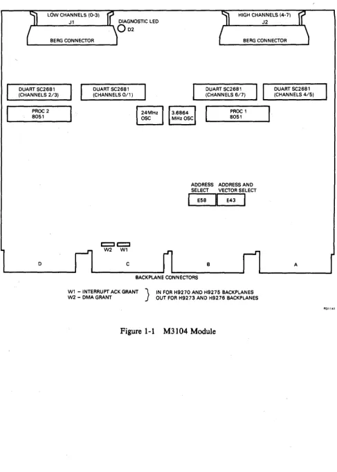
The option is based on a standard quad-height module (M31 04). The layout of this module is shown in Figure 1-1. The dimensions are 21.6 cm x 26.5 cm (8.51 inches x 10.44 inches).
The, module is connected to the Q-bus via connectors A and B. 11 and J2 are connected to the communications lines via BC05 L-xx cables and H31 73-A distribution panels.
On some backplanes, jumpers WI (BIAK) and W2 (BDMG) extend the bus grant signals to the next module slot via connectors C and D.
LOW CHANNELS (0-3) Jl
BERG CONNECTOR
HIGH CHANNELS (4-7) J2
BERG CONNECTOR
DUART SC2681 (CHANNELS 2/3)
DUART SC2681 (CHANNELS 011)
DUART SC2681 (CHANNELS 617)
DUART SC2681 (CHANNELS 4/5)
PROC 2 8051
D C
I
24MHzI
OSCPROC 1 8051
ADDRESS ADDRESS AND SELECT VECTOR SELECT
I
E58~
E43I
B
BACKPLANE CONNECTORS
Wl - INTERRUPT ACK GRANT } IN FOR H9270 AND H9275 BACKPLANES W2 - DMA GRANT OUT FOR H9273 AND H9276 BACKPLANES
Figure 1-1 M3104 Module
1-3
A
[image:15.597.45.533.48.730.2]1.2.3 Versions of DHVll
To facilitate installation in different system packages, and to allow installation in non-specified cabinets, the DHVll module (DHVII-M) can be supplied with one of three cabinet kits. Except for the length of the flat ribbon cables, the cabinet kits are the same.
DHVII-M is made up of the following:
• The module
• This technical manual
M3104
EK-DHVlI-TM • Packaging.
The three cabinet kits are:
• CK-DHVII-AA (21-inch cables); example of use, PDP-l1/23S • CK-DHVlI-AB (12-inch cables); example of use, Micro/PDP-lI • CK-DHVlI-AC (30-inch cables); example of use, PDP-1I!23 PLUS Each kit is made up of:
• Two BC05L-xx cables (see NOTES) • H325 line loopback connector • H3277 staggered loopback connector
• Two H3173-A distribution panels (see NOTES) • Mounting bolts and washers for H3173-A. • Adapter plate (contained in CK-DHVII-AC)
NOTES
The H3173-A distribution panels provide noise filtering and static discharge protection on the communications lines.
BC05L-xx cables are supplied in different lengths for each kit. The kits are specified in Section 2.2. DIGITAL does not supply a cabinet kit for installing the DHVll in non-FCC-compliant cabinets.
The hardware is connected as in Section 1.2.5.
1.2.4 Configurations
HOST }
PROCESSOR~~SY_S_T_EM~B_U_S_(_Q2~2~O_R_LS_I_l_l) ________________________ ~
>-
"'>-
.~.
"
DEVICE DEVICE
r--- r--- r--- r---
-~
I
,.-.-~'---...
I
M3104 MODULE
LOCAL EQUIPMENT
I
1
I
I
REMOTE EQUIPMENT
I
I
I
I
f
I
I
I
I
\
MODEM TELEPH~NE .. OR_MODEM 1_ r---_ REMOTE TERMINAL
I
I
DATACOMMS
'----~ LINE
I
, 8 DATA CHANNELS
I
LD~12.. O~I~ _
, LOCAL
L---Ir-~ TERMINAL
_I
\
,
I
I
TELEPHONE OR
---
I
I
MODEM
4-' - -_ _ ~ DATA COMMS LINE I
L _ _ _
_ _ _ _ _ _ _
.J
MODEM _ REMOTE DHVll
REMOTE
PROCESSOR ~ __________________ Q2_2_0_R __ LS_I_l_l_B_US ____________________________ __
R01142
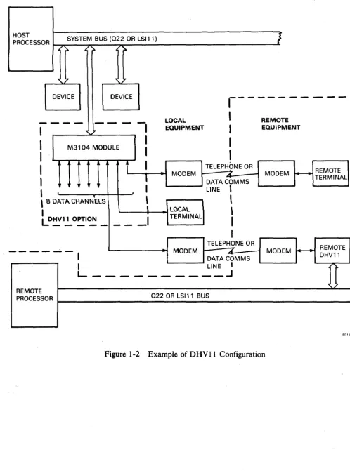
Figure 1-2 Example of DHVII Configuration
[image:17.594.43.541.52.722.2]1.2.5 Connections
Figure 1-3 shows the connections for the DHV11. These include normal operating connections and test connections. More detail is shown in Figure 2-3 in Section 2.
...
"
"
\
H3277 \
U'
TEST
-STAGGERED
~;_~
LOOPBACKCONNECTOR
n
,~~~~~
/1
~
...
_--
/
~ = NORMAL CONNECTION ...,. = TEST CONNECTION
NOTE: BC05L~01
=
30.48 CM (12 INCHES) BC05L-1 K=
53.34 CM (21 INCHES) BC05L-2F=
76.2 CM (30 INCHES).,/
Figure 1-3 DHV11 Connections
1.3 SPECIFICATION
1.3.1 Environment Conditions
• Storage temperature: O°C to 66°C (32°F to 151°F) • Operating temperature: 5°C to 60°C (41°F to 140°F) • Relative humidity: 10% to 95% non-condensing
H325 LINE
}
CHANNELS 0-3
25 PIN D TYPE CONNECTORS
CHANNELS 4-7
LOOPBACK TEST CONNECTOR
1.3.2 Electrical Requirements
+5 V dc
+
or - 5% at 4.25 A (typical) +12 V dc+
or - 20% at 520 rnA (typical)Negative 12 V dc is generated by a Switched Mode Power Supply (SMPS) circuit on the DHV11.1t has the following specification:
-11.85 V dc + or - 7.25% at 400 rnA (maximum) Output ripple is 200 mV peak to peak at 36.7 kHz
Loads applied to the Q-bus are as follows: Q-bus ac loads
Q-bus dc loads
1.3.3 Performance
2.9 ac loads 1.0 dc loads
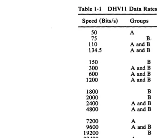
1.3.3.1 Data Rates - Each channel can be programmed to operate at one of a number of speeds. If needed, th~ transmission and reception rates can be different (split speed). Table 1-1 shows the data rates which are'possible. The maximum rate per channel is 38400 bits per second (bits/s).
The eight serial channels are implemented with four DUART ICs (Integrated Circuits). Channels are paired as follows: 0/1, 2/3, 4/5, 6/7. Because of the method of data rate generation, all transmit and receive rates for a DUART channel-pair must be in the same group (A or B).
Table 1·1 DHV11 Data Rates
Speed (Bits/s) Groups
50 A
75
R
110 AandB
134.5 AandB
150 B
300 AandB
600 AandB
1200 AandB
1800 B
2000 B
2400 AandB
4800 AandB
7200 A
9600 AandB
19200 B
38400 A
Data rate selection is covered in Chapter 3 (Programming).
[image:19.603.61.397.379.665.2]1.3.3.2 Throughput - Each channel is capable of full-duplex operation at data rates of up to 38400 bits/so The DRVll, however, cannot handle eight channels operating at this rate at the same time. Total maximum throughput is also dependent on the application and configuration.
Maximum throughput:
Per channel (send) 1000 characters per second in single-character transfer mode
2000 characters per second in DMA mode
(receive) 4000 characters per second.
On any channel, the DRVII can send at one of the above transmit rates and receive at 4000 characters per second at the same time.
Total (8 channels)
1.4 INTERFACES
15000 characters per second NOTES
The DMA firmware cannot handle transmit data faster than 2000 characters per second (19200 bits/s). If the transmit data rate is increased to 38400 bits/s, the duration of each character will be halved but there will be gaps in transmission. 15000 characters per second is the sum of both transmitted and received characters on all channels. This throughput could support all channels transmitting or receiving at 19200 bits/ s, or all channels transmitting and receiving at 9600 bits/ s. The above figures are based on a 7- bit character with start bit, parity bit, and one
stop
bit.
1.4.1 System Bus Interface
The M3104 module will connect directly to the Q-bus via connectors A and B. To make the module compatible with backplanes which have Q-bus on C and D also, two jumpers (W 1 and W2) are provided. The use of these jumpers is described in Section 2.3. Backplane signals, together with pin details, are listed in Table 2-3.
1.4.2 Serial Interfaces
1.4.2.1 Interface Standards - The DRVII provides interface signals which conform to a subset of the EIA/CCITT standard RS-232-C/V.24. The electrical characteristics conform to EIA/CCITT standards RS-232-C/V.24 and RS-423-A/V.28 (unbalanced interface). The interface is compatible with X.26/V.I0 standards but does not comply with the slew rate requirements.
By means of suitable cables and connectors (not supplied or supported by DIGITAL) the channels can be made compatible with the following:
1. Subset of EIA interchange standard RS-449 2. EIA electrical standard RS-422 (balanced).
NOTE
Even when RS-422 is implemented; RS-423-A cable length/data rate recommendations should be followed.
The distribution panel does not support split grounds.
Table 1-2 shows RS-232-C/V.24/RS-449 signal relationships, and pin connections for the male subminiature D-type connectors.
Table 1-2 EINCCITT Signal Relationships
Signal D-Type RS-232-C Circuit Circuit
Name Pin CCITIV.24 RS-449
Protective Ground (GND) 1 AA
Signal Ground (SIG GND) 7 AB 102 SG
Transmitted Data (TXD) 2 BA 103 SD
Received Data (RXD) 3 BB 104 RD
Request to Send (RTS) 4 CA 105 RS
~
Clear to Send (CTS) 5 CB 106 CS
Data Set Ready (DSR) 6 CC 107 DM
Data Terminal Ready (DTR) 20 CD 108/2 TR
Ring Indicator (RI) 22 CE 125 IC
Data Carrier Detect (DCD) 8 CF 109 RR
NOTE
,
The backward channels listed below are not supported. However, by using another channel for this function, and by connecting a suitable cable (H1200 or H1201 for example), backward channel operation is possible.
Circuit No.
118
120
119
121 122
Function
Transmitted backward channel data Transmit backward channel line signal Received backward channel data Backward channel ready
Backward channel received line signal detector
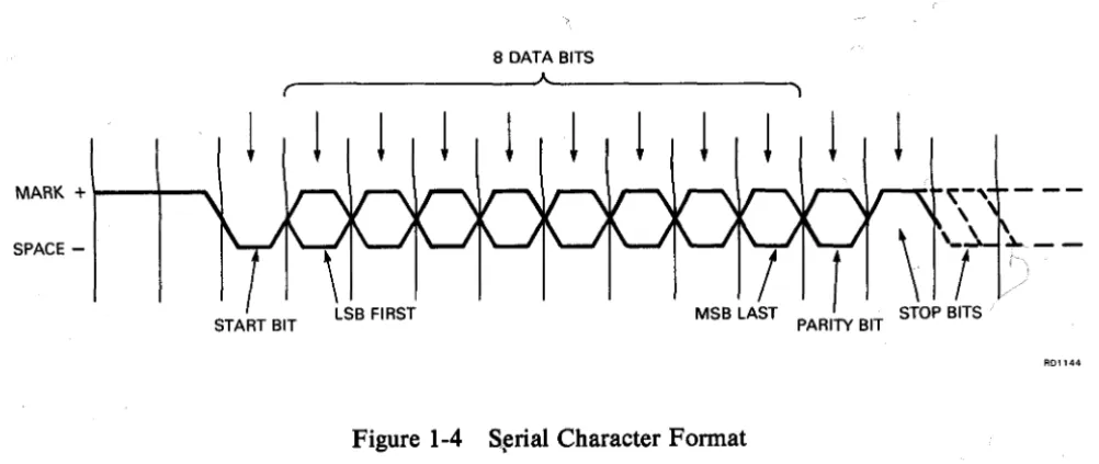
1.4.2.2 Serial Data Format - Serial characters are made up of a coded sequence of bits which are enclosed between a start and a stop signal. The start signal is always 1 bit long but the stop signal is programmable to 1, 1.5, or 2 bits. The duration of a bit is dependent on the selected data rate.
Character codes may be 5, 6, 7, or 8 bits long, optionally followed by a parity bit. Parity can be programmed as even, odd, or no parity.
Ori serial data channels controlled via the D HV 11, the data line is held marking when inactive. Transfer of each character begins with a start bit (space) and ends with one or more stop bits (mark).
Figure 1-4 shows the reception of an 8-bit character with parity. The Least-Significant Bit (LSB) of the character code is transmitted first. If another character is not ready for transmission, the line will stay marking. The figure shows 1, 1.5, and 2 stop bits.
NOTE
This description applies to signals at the DUART pins. Signals measured on the interchange circuits will have the opposite polarity to those shown.
The data rate clock which times the serial data, is 16 times the programmed data rate. Arrows show when the bits are tested for polarity.
8 DATA BITS
~ ______________ -JA~ ______________ ~
r )
!
!
!
! ! !
!
! !
!
MARK + l--+-~
SPACE
-START BIT PARITY BIT
Figure 1-4 S~rial Character Format
The DHV11 allows the following serial character formats:
• Characters of 5, 6, 7, or 8 bits with or without parity and with 1 stop bit
!
[image:22.594.52.553.426.637.2]1.4.2.3 Line Receivers - The serial line receivers used in this module are 9637 AC or equivalent. They convert the EIA input signals to TTL levels suitable for the DUARTs.
Signals are· inverted by the receivers.
1.4.2.4 Line Transmitters - The serial line transmitters used in this module are 9636AC or equivalent. They convert TTL level signals from the DUARTs to EIA levels on the data lines.
Signals are inverted by the transmitters.
1.4.2.5 Speed/Distance Considerations - The maximum data rate which can be used on a line depends upon a number of factors. These are:
1. The characteristics of the line transmitters and receivers 2. The characteristics of the serial cable (or link)
3. The length of the cable
4. Noise (interference) which affects the line.
A 'speed against distance' table for typical conditions is provided in Section 2.6.6.
022/LSI11 BUS INTERFACE DMA INTERRUPT AND PROTOCOL LOGIC BUS DRIVERS AND RECEIVERS 110 ADDRESS CONTROL SECTION DMA REOUEST
DMA ADDRESSES AND DATA
DATA AND CON FIG
FIFO
CONTROL ~~_...,
RECOG - /o:R~EA~D:-A~D:-::D:::'RE=::S:::::S~E~NA~B~LE NITION 1
I
1 I
~ 1
WRITE ADDRESS ENABLE
1--- - - I
1 RAM 1
REGISTERS
I
AND BUFFERS1 1 1 1 1
1---1FIFO 1
(256 CHARS) 1
0...-_ _ ... 1 __ J
Figure 1-5 DHVll Functional Block
1-11
SERIAL INTERFACES
.~ w Z Z <I: J: U X W ...J Il. ::J o co
1.5 FUNCTIONAL DESCRIPTION
1.5.1 Control Function
In the DHVII module (Figure 1-5), data is transferred by three methods:
1. By DMA. Blocks of data are transferred from system memory to the serial interface. DMA data is routed via the bus receivers, PROC1, the RAM, and PROC2.
2. In the non-DMA mode, single characters can be transferred from the host system to the serial interface. The route for single characters is via the bus receivers, the RAM, PROC 1 , the RAM, and PROC2.
3. Single characters can be transferred from the serial interface to the host system. The route for received characters is via PROC2, the FIFO buffer, and the bus drivers.
At the center of the control section is a 1 K-word RAM. By writing control words to registers in the RAM, the host can indirectly configure and command the module. The host can also write data bytes to registers in the RAM.
Two microcomputers (PROC 1 and PROC 2), which contain their own programs in internal ROM, scan the RAM in order to detect a new configuration, or data to be transferred. They also write status information to the RAM, which can then be read by the host.
PROC 2 configures the DUARTs as instructed, and transfers transmit and receive data between the RAM and the DUARTs. Received characters are writteri to FIFO addresses provided by FIFO control.
Among other functions, PROC 1 controls DMA actions. Using DMA information provided by the host, it starts DMA circuits which control each DMA transfer. PROC 1 keeps track of DMA addresses and character count, and reports to the host when the block has been transferred.
Both microcomputers execute· background diagnostics when not busy with other tasks. 1.5.2 Q-Bus Interface
The DHVII module is considered by the host system as a number of I/O ports. The bus drivers and receivers recognize DHVII addresses and allow the host to access the FIFO buffer and the registers. When the FIFO buffer is being read, FIFO control provides the read addresses.
Standard DIGITAL LSI protocol, interrupt, and DMA integrated circuits (ICs) control the interface.
Module address switches are connected to comparators in the bus driver/receiver ICs. When an I/O address from the host is the same as the address on the switches, the DHV11 responds to the host. On receiving the response, the host proceeds with the transaction.
Vector address switches are also connected to the bus drivers. These allow the DHVll to supply two interrupt vectors (transmit and receive) to the host during an interrupt acknowledge sequence.
1.5.3 Serial Interfaces
2.1 SCOPE
CHAPTER 2
INSTALLATION
This chapter contains information on how to prepare and install the DHVII option. It contains sections on the following:
• Device and vector address selection • Rules for backplane positioning • Recommended cables
• Test connectors
• Floating address and vector assignment • Testing after installation.
2.2 UNPACKING AND INSPECTION
There are a number of versions of the DHVll, all of which are based on the module kitDHVII-M. This may be ordered with one of the three cabinet kits listed below. Examine all parts for physical damage. Report damaged or missing items to the shipper and the DIGITAL representative.
DHVII-M
DHVll"AP
M3104 + EK-DHVII-TM, (field upgrade base option)
System integrated DHVII
(DHVII-M + appropriate cabinet kit)
Field Upgrade Cabinet Kits
CK-DHVI1-AA PDP-l1/23S systems
CK-DHVII-AB MicroPDP-ll and Micro V AX systems CK-DHVII-AC PDP-ll/23+ systems
Contents
H325 Single line loopback H3277 Staggered loopback
H3173A 4-line 25-way distribution panel BC05L-IK 40-way ribbon cable, 21 inch BC05L-O1 40-way ribbon cable, 12 inch BC05L-2F 40-way ribbon cable, 30 inch 74-28684-01 Adapter plate
90-06021-01 Bolt 90-06633-00 Washer
2-1
1
11
1 11 1 1 2 2 2 2 2 2 2
2.3 INSTALLATION CHECKS
2.3.1 Address Switches
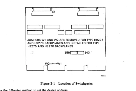
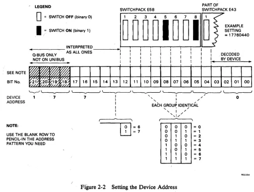
The device address for the DHVII is set on switchpacks E58 and E43. The location of these switchpacks is shown in Figure 2-1. Figure 2-2 shows the method of setting the device address on the switchpacks. The example shown is for a Q22-bus address of 177604408.
From the information contained in Figure 2-2 it can be seen that switches 5 and 8 on switchpack E5 8 must be set to ON for the example shown.
~==:::::I
L.-I _---..II
I~;:::::=::::::.I ~I
_---'
1..---11
D D
1
JUMPERS Wl AND W2 ARE REMOVED FOR TYPE H9276 AND H9273 BACKPLANES AND INSTALLED FOR TYPE H9275 AND H9270 BACKPLANES
[image:26.588.68.535.171.483.2]E58
c:::x:::J
E43Figure 2-1 Location of Switchpacks
Use the following method to set the device address.
R02342
1. Define the octal address. This mayor may not be the factory default, and will depend upon what other devices are contained within this system configuration. Refer to Table 2-4 for information on floating device address assignments.
2. Convert the octal address to a binary bit pattern. You can write this pattern on Figure 2-2, in the blank character line left for this purpose.
SEE NOTE
BIT No.
DEVICE ADDRESS
NOTE:
LEGEND
o
= SWITCH OFF (binary 0)PART OF
SWITCH PACK E58 SWITCHPACK E43
1 2 3 4 5 6 7 8 1
EXAMPLE SETTING
I
j= SWITCH ON (binary 1)000010010
=
17760440.. INTERPRETED _ _ _ ---I .. ~I-T-ii-ii--r-I-JI'-~
Q-BUS ONLY AS ALL ONES I
I .
DECODEDNOT ON UNIBUS I I BY DEVICE
.. • I
1 ' - .
~
~
~
~
~f~~
C/O"
~/~~~~
17 16 15 14 13 12 11 10 09 08 07 06 05 04 03 02 01 00~J- v2 }, I/} 9.1 .~
'---' L--...---J ~ ~ ~ "---..".--.~ '---...----.J
1 7 7 I .... I / ' 0
I .... , I /
I
I EACH GROUP IDENTICAL
,
.
/
I , I /
I ' .... 1//
~--~~-~, ~-~
0 0 0 0 0 1 USE THE BLANK ROW TO
PENCIL-IN THE ADDRESS PATTERN YOU NEED
I
01
= 6I2J
= 70 0 1
1 1 0
0 1 0
=0 = 1
= 2
= 3
= 4
= 5
= 6 = 7 1 0 1 1 1 0 1 1 1
[image:27.597.44.556.54.441.2]RD2254
Figure 2-2 Setting the Device Address
2.3.2 Vector Switches
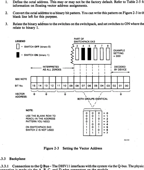
During an interrupt acknowledge sequence, the DHVII returns a 7 -bit interrupt vector to the host The six high-order bits of this vector are derived from the settings of the last six switches of switch pack E43. The location of this switchpack is shown in Figure 2-1. Figure 2-3 provides an example of these switches set to an address of 3008. From the information in Figure 2-3 it can be seen that switches 4 and 5 must be set to ON for the example shown.
You can use t4e following method to set up the vector address.
1. Define the octal address. This mayor may not be the factory default Refer to'Table 2-5 for information on floating vector address assignments.
2. Convert the octal address to a binary bit pattern. You can write this pattern on Figure 2-3 in the blank line left for this purpose ..
~
3. Relate the binary address to the switches on the switchpack, and set switches to ON where they relate to binary 1.
LEGEND
D
= SWITCH OFF (binary 0)I
= SWITCH ON (binary 1 )... _ _ INTERPRETED AS ALL ZEROES
SEE NOTE
BIT No. 15 14 13 12
VECTOR 0
o
ADDRESS:
NOTE:
USE THE BLANK ROW TO PENCIL-IN THE ADDRESS PATTERN YOU NEED
. ON SWITCH PACK E43 SWITCH 2 IS NOT USED
11 10 09
o
PART OF
SWITCHPACK E43
3 4 5 6 7 8
011000
08 07 06 05 04 03
\ /
\ I
BOTH GROUPS IDENTICAL
\ '
\ /
\ /
~
0 0 0 0 0 1 0 1 0 0 1 1 1 0 0 1 0 1 1 1 0 1 1 1
= 0
= 1
= 2 = 3
== 4
= 5
= 6
[image:28.588.59.527.76.628.2]= 7
Figure 2-3 Setting the Vector Address
2.3.3 Backplane
EXAMPLE SETTING =300
I DECODED I BY DEVICE
I" ..
02 01 00
o
R02255
2.3.3.1 Connection to the Q Bus - The DHV11 interfaces with the system via the Q-bus. The physical connection is made via the A, B, C, and D edge connectors on the module.
Table 2-1 DHVII Bus Connections
Category Signal Function Pin Number
Datal Address BDALO.L - 1.L Datal Address Lines AU2-AV2
BDALl.L - l5.L BE2 - BV2
BDAL16.L - l7.L ACl- ADI
BDAL18.L - 21.L BCl - BFl
Data Control BDOUT.L Data Output Strobe AE2
BRPLY.L Reply Handshake AF2
BDIN.L Data Input Strobe AH2
BSYNC.L Synchronize Strobe AJ2
BWTBT.L Write Byte Control AK2
BBS7.L I/O Page Select AP2
Interrupt Control BIRQ.L Int. Req. Level 4 AL2
BIAKI.L Int. Ack. Input AM2
BIAKO.L Int. Ack. Output AN2
>::11!',
DMA Control BDMR.L DMA Request ANI
BDMGI.L DMA Grant Input AR2
BDMGO.L DMA Grant Output AS2
BSACK.L Bus Grant Acknowledge BNl
System Control BINIT.L Initialization Strobe AT2
I J
Power Supplies +5 V DC Volts AA2-DA2
+12 V DC Volts BD2
Grounds GND Ground Connections AC2-DC2
GND , Ground Connections ATI - DTI
GND Ground Connections AJl - BJ1
GND Ground Connections AMl-BMl
2.3.3.2 Bus Grant Continuity Jumpers - Backplanes suitable for DHVII fall into two groups:
Q/CD Q/Q
-Q-bus on A and B connectors, user-defined signals on C and D Q-bus on A and B, and C and D connectors.
In Q/CD backplanes, bus grant signals pass through each installed module via the A and B connectors of each bus slot.
Q/Q backplanes are designed so that two dual-height options can be installed in a quad-height bus slot. The Q-bus lines are routed as follows:
AB, first slot CD, first slot CD, second slot
AB, second slot and so on.
Lihes AM2, AN2, CM2, and CN2 (BIAK) and AR2, AS2, CR2, and CS2 (BDMG) carry the bus grant signals .. Figure 2-4 uses BIAK as an example of bus grant routing. The same method is used for continuity ofBDMG.
Q/Q BACKPLANE
r----...,
Wl EXTENDS BIAKQ/CD BACKPLANE
- - - I
MODULE 1 1
I
1
CN2 1 / CN2
: CN2
CN2 I
I
IC ID
I
INTERRUPT 1 CONTROL I1
11
CM2 1L __ __-.J
1---
- - - I1
1
AN2 11
1
AlB 1 INTERRUPT CONTROL I
BIAK
I 1
I 1
AM2
I
DUAL
L _ M...9D~L!. _ J
SLOT
1
,n
I
1 I
Wl 1
1
I
CM2 :
I I
1 1
1
1AN2 [
1 1
1
1
INTERRUPT I
1 CONTROL
I
1I
AM2 II QUAD I
L_~~LI. _I
SLOT
I
lSHORT'CIRCUIT~ 1 IF INSTALLED Wl I
C/D
I
ICM2 CM2
1 - - - - ,
AN2 AN2
I
I I 1
1 1
1
~.
AlB
I INTERRUPT
1 INTERRUPT 1
I CONTROL
1
CONTROL 1
1
I lAM2 1
IAM2
I
I 1
I 1
"---;:?
BIAK
AM2 DUAL
L_M.ED~~
J
1 L _M.2P~E QUAD _ _ IM2
SLOT SLOT
-~o--BACKPLANE
• MODULE WIRING
AD1S39
Figure 2-4 Bus Grant Continuity
Each dual-height module will extend the continuity of bus grant signals BIAK and BDMG to the next module. .
If a quad-height option is installed,jumpers perform the grant continuity function of a dual option installed on C and D.
Therefore, with a Q/Q backplane, WI and W2 should be installed. H9275 and.H9270 are examples of this type of backplane.
In a Q/CD backplane, pins CM2, CN2, CR2, and CS2 are available for user-defined signals. Therefore WI and W2 must be removed. H9276 and H9273 are examples of this type of backplane.
2.4 PRIORITY SELECTION
2.4.1 D MA Request
DMA request priority is usually selected on a basis of throughput. The faster devices (higher throughput) will usually have priority over slower DMA devices; for example, disk, tape, and then communications devices. This is because a fast device will usually reach an overrunlunderrun condition sooner than a
slower device. . .
The simple approach can be further complicated by hardware buffering in the device. For example, a disk controller may read a full sector of information into a hardware buffer. It may then raise a DMA request to . move the data to system memory. If the request is not serviced immediately, there is no danger of data loss. However, a magnetic tape unit or a communications device without buffering may need to be serviced quickly. In this case the slower unit might be serviced first. This method of priority selection could, of course, reduce disk throughput.
The system designer should consider the following four factors in determining DMA priorities:
1. Device average service time
2. Maximum wait time to be allowed (before loss of data) 3. Average time between DMA requests
4. Slack time.
Using the above parameters, the system designer should assume that all DMA requests are made at the same time. He should then check that his selected priority sequence does not violate the parameters of any DMA device.
If there is only one DMA device in the system there is no DMA contention. The device's position on the bus will be determined by its interrupt (BIRQ) priority.
NOTE
If the system memory needs refresh cycles via the bus, these should be considered as DMA requests.
2.4.2 Interrupt Request
Interrupt requests have four levels of priority. The lowest is Level 4 and the highest is Level 7. Requests· are made on bus interrupt request lines BIRQ4 to BIRQ7. To avoid,contention, lower-priority devices usually monitor the higher request lines.
Within any priority group, priority is decided by backplane position. The most time-critical interrupts must be nearer the CPU.
There are two common types of configuration for devices which need interrupt service:
1. The position-independent configuration 2. The position-dependent configuration.
In the position-independent configuration, devices of different priority groups can be placed anywhere in the backplane.
In the position-dependent configuration, devices of different priority groups are positioned in descending order of priority from the CPU.
Because the DHVll is a Level 4 device which does not monitor higher request lines, it must be positioned after all devices that do. Therefore DHVll priority is position dependent in either configuration.
By assuming that all interrupts are raised at the same time, the system designer can check his priority sequence as for DMA requests.
2.5 MODULE INSTALLATION
Once the backplane position of the DHVII has been defined, the module can be installed and the backplane checked with a testmeter.
CAUTION
Switch off power before inserting or removing modules. Be careful not to snag module components on the card guides or adjacent modules.
LL. L.LJ o u
RED LINE TOA
PIN A
~ = NORMAL CONNECTION
~ = TEST CONNECTION
RED LINE TOA
"
"
" \ RED LINE H3277 \
V'
TO A STAGGEREDOR--~~J1
LOOPBACKTEST - - J2
CONNECTOR r i
/ \ ~
... , /
---
/_ . / RED LINE
A
NOTE: BC05L-01 = 30.48 CM (12 INCHES) BC05L-1 K= 53.34 CM (21 INCHES) BC05L-2F = 76.2 CM (30 INCHES)
CHANNELS 0-3
H3 3-A DISTRIBUTION PANEL
1
CHANNELS 4-7
H325 LINE
LOOPBACK TEST CONNECTOR
Figure 2-5 DHVII Installation
A. PRINTED ON PCB
1. Connect the BC05L cables to J1 and 12. Figure 2-5 shows how the parts ofthe option connect together.
2. Install the module in its correct backplane position as defined in Section 2.4.
3. Check that
+
5 V is present between AA2 and ground.4. Check that
+
12 V is present between BD2 and ground. 2.6 CABLES AND CONNECTORS2.6.1 Distribution Panel
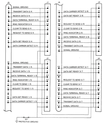
Each H3173-A distribution panel adapts one of the DHVll 's berg connectors to four subminiature D-type RS-232-C connectors. Noise filtering is provided on each pin of the RS-232-C connectors. This reduces electromagnetic radiation from the cables. It also provides the logic with some protection against static discharge.
Figure 2-6 shows the layout and Figure 2-7 shows the circuit. There is no CCITT equivalent of EIA circuit AA (protective ground). The O-ohm link WI can be removed to disconnect this circuit as needed.
Table 2-2 is for two distribution panels. Information in parentheses applies to channels 4 to 7.
E
c-u ~
00
~
"
~
2-c-
c-o
0M ~
M
-E E
u u
00
"
M L!)
a:i <i
O~===I==~
1-~---LI----P~9
b~
~d
METAL PLATE
FILTERED D-TYPE (x4)
SCREWLOCK (x8)
J1
~PCB
THREADED INSERT (x4)
_J,h ___ - U - - - -FOR 6-32
- - - BOLT
90-06021-01
J2
J3
----~---~~-- - - -- - - _ _ BERG (J5)
J4
2.62em
I (1.031in)
5.24em (2.062in)
NOT DRAWN TO SCALE
6.60em (2.60in)
RD1146
Figure 2-6 H3173-A Layout
The following is an example of the use of Table 2-2.
Signal TXDO is the Transmitted Data line for channel O. Its CCITT circuit number is 103. It is connected to J5 pin B on the H3173-A for channels 0 to 3.
Signal TXD4 is the Transmitted Data line for channel 4. Its CCITT circuit number is 103.1t is connected to J5 pin B on the H3173-A for channels 4 to 7.
J5 J1 J5 J3
.---
rr"-/
r-~ SIGNAL GROUND 7 1
--B TRANSMIT DATA 0/4
..
2..
Y DATA CARRIER DETECT 2/6 8 C RECEIVE DATA 0/4 3 Z DATA SET READY 2/6 6" .
.!2 DATA TERMINAL READY 0/4 2_0 AA
-
•
E RING INDICATOR 0/4
2J
BB REQUEST TO SEND 2/6 4r
CLEAR TO SEND 0/4 ~ CC CLEAR TO SEND 2/6 5-
HREQUEST TO SEND 0/4 4 DD ,.. RING INDICATOR 2/6 22
" .
J EE
•
DATA TERMINAL READY 2/6 20~ DATA SET READY 0/4 ~ ~ RECEIVE DATA 2/6 3 L DATA CARRIER DETECT 0/4 8 HH TRANSMIT DATA 2/6 2
" .
2.
-!j SIGNAL GROUND..
7-
"-~ ~
M SIGNAL GROUND 7
1.
-!;! TRANSMIT DATA 1/5 2 KK DATA CARRIER DETECT 3/7 8
r
RECEIVE DATA 115 ~ LL DATA SET READY 3/7 6 --R DATA TERMINAL READY 115 22 MM•
~ RING INDICATOR 115 22 N..N REQUEST TO SEND 3/7 4
,..
--r
CLEAR TO SEND 1/5..
5 ~ CLEAR TO SEND 3/7 5U REOUEST TO SEND 1/5 1: RR
..
RING INDICATOR 3/7 22 V SS DATA TERMINAL READY 3/7 2_0•
W DATA SET READY 1/5 ~ If RECEIVE DATA 3/7 3 X DATA CARRIER DETECT 115 ~ UU TRANSMIT DATA 3/7 ~
2.
V_V SIGNAL GROUND 7"
-
,
' - - - - L .-~
W1 [image:34.591.80.509.151.661.2]Table 2-2 H3173-A Connections
Signal Name Circuit No. J5 Pin No.
SIG GND 0(4) 102 I-A (2-A)
TXDO(4) Transmitted Data 103 I-B (2-B)
RXDO(4) Received Data 104 l-C (2-C)
DTRO(4) Data Terminal Ready 108/2 I-D (2-D)
RIO(4) Ringing Indicator 125 l-E (2-E)
CTSO(4) Clear to Send 106 I-F (2-F)
RTSO(4) Request to Send 105 I-H (2-H)
DSRO(4) Data Set Ready 107 l-K (2-K)
DCDO(4) Data Carrier Detected 109 l-L (2-L)
SIGGND 1(5) 102 I-M (2-M)
TXDl(5) 103 I-N (2-N)
RXDl(5) 104 I-P (2-P)
DTRl(5) 108/2 l-R (2-R)
RIl(5) 125 I-S (2-S)
CTSl(5) 106 I-T (2-T)
RTSl(5) 105 l-U (2-U)
DSRl(5) 107 l-W (2-W)
DCDl(5) 109 I-X (2-X)
DCD2(6) 109 l-Y (2-Y)
DSR2(6) 107 l-Z (2-Z)
RTS2(6) 105 I-BB (2-BB)
CTS2(6) 106 l-CC (2-CC)
RI2(6) 125 I-DD (2-DD)
DTR2(6) 108/2 l-EE (2-EE)
RXD2(6) 104 I-FF (2-FF)
TXD2(6) 103 I-HH (2-HH)
SIG GND 2(6) 102 I-JJ (2-JJ)
DCD3(7) 109 l-KK (2-KK)
DSR3(7) 107 l-LL (2-LL)
RTS3(7) 105 I-NN (2-NN)
CTS3(7) 106 I-PP (2-PP)
RI3(7) 125 l-RR (2-RR)
DTR3(7) 108/2 I-SS (2-SS)
RXD3(7) 104 I-TT (2-TT)
TXD3(7) 103 l-UU (2-UU)
SIG GND 3(7) 102 I-VV (2-VV)
2.6.2 Staggered Loopback Test Connector H3277
(See Figure 2-8.) The H3277 test connector is used during diagnostic tests. It allows all channels to be tested. Using this connector, you can trace a channel fault to one of two channels.
Jl J2
S TXDO TXD4 B FF RXD2
t
t
RXD6 FFHH TXD2 TXD6 HH
C RXDO
t
f
RXD4 CD~
ED
DD DD
Z DSR2 DSR6 Z
EE DTR2 DTR6 EE
'=::3
~,
K DSRO DSR4 K
"=:B E"
cc cc
y DCD2 DCD6 Y
.--
... SS RTS2 RTS6 SS0:: 0::
F
=:B
E
0 0F f--
f--U u
DCDO DCD4 LU LU
L L z z z z
TXDl TXD5 0 0
N u u
t
t
N t9 t90:: 0::
RXD3 RXD7 LU LU
TT TT m m
Z Z
UU TXD3 TXD7 UU ii: ii:
t
f
0 0RXDl RXD5 '<t '<t
P P
'~
E2='
----
Jl---
J2RR RR
DSR3 DSR7 PHYSICAL ARRANGEMENT
LL LL
SS DTR3 DTR7 SS
s~
~s
W DSRl DSR5 W
u~
ED
PP PP
KK DCD3 DCD7 KK
NN RTS3 RTS7 NN
T=:g ET
X DCDl DCD5 X
2.6.3 Line Loopback Test Connector H325
This connector is shown in Figure 2-9. It can be used during diagnostic tests to trace a fault to a single channel.
CCITT No. NAME PIN
24
NOT USED
~
15 NOT USED
NOT USED 17
11 NOT USED
-,
12NOT USED
TXD 2
103 ~,
RXD 3 104
RTS 4 105
B
106 CTS
109 DCD
NOT USED 14
107 DSR 6
108.2 DTR 20
RI 22 125
CONNECTIONS
W1
W1
(~
O
\(···u
\\ • • • • • • • • • • • • J Io
JH325
PHYSICAL ARRANGEMENT
W1 IS PERMANENTLY IN FOR DHV11 TESTING
RD1149
Figure 2-9 Line Loopback Test Connector 2.6.4 Null Modem Cables
Null modem cables are used for local RS-232-C connection. Because of Federal Communications Commission (FCC) regulations, the cable specifications for the United States and Canada are different from those for non- FCC countries. Other countries may also have similar ElectroMagnetic Interference (EMI) control regulations. EMC/RFI shielded cabinets (see glossary) are now available for systems which conform to FCC requirements.
Recommended null modem cables are as follows:
1. BC22D (for EMC/RFI shielded cabinets)
• Round 6-conductor fully shielded cable to FCC specification • Subminiature 25-pin D-type female connector moulded on each end • Lengths available:
BC22D-I0 BC22D-25 BC22D-35 BC22D-50 BC22D-75 BC22D-AO BC22D-B5
- 3.1 m (10 ft) - 7.62 m (25 ft) - 10.72 m (35 ft)
- 15.24 m (50 ft)
- 22.9 m (75 ft)
- 30.48 m (100 ft)
- 76.2 m (250 ft).
2. BC03M
• Round 6-conductor (three twisted pairs), each pair shielded
• Cables over 30.48 m (100 ft) have a 25-pin subminiature D-type female connector at one end. The other end is unterminated for passing through conduit.
• Cables 30.48 m (100 ft) and less have a similar connector at each end. • Lengths available:
BC03M-25 BC03M-AO BC03M-B5 BC03M-EO BC03M-LO
- 7.62 m (25 ft)
- 30.48 m (100 ft) - 76.2 m (250 ft) - 152.4 m (500 ft)
- 304.8 m (1000 ft).
3. BC22A
•
•
•
Round 6-conductor cable
Subminiature 25-pin D-type female connector moulded at each end Lengths available:
BC22A-1O - 3.1 m (10 ft)
BC22A-25 - 7.62 m (25 ft).
PIN PIN
NUMBERS NUMBERS
1 0 PROTECTIVE GROUND PROTECTIVE GROUND 01
20 TRANSMITIED DATA RECEIVED DATA 03
3 0 RECEIVED DATA TRANSMITIED DATA 02
7 0 SIGNAL GROUND SIGNAL GROUND
o
760 DATA SET READY DATA TERMINAL READY 020
20 0 DATA TERMINAL READY DATA SET READY 06
RU1150
Figure 2-10 Null Modem Cable Connections
2.6.5 Full Modem Cables
Recommended full modem cables are as follows:
1. BC22F (for EMC/RFI shielded cabinets) • Round 25-conductor fully shielded cable
• Subminiature 25-pin D-type female connector on one end, male connector on the other • Lengths available:
BC22F-1O BC22F-25 BC22F-35 BC22F-50 BC22F-75
- 3.1 m (10 ft)
- 7.62 m (25 ft)
- 10.72 m (35 ft)
- 15.24 m (50 ft)
- 22.9 m (75 ft) 2. BC05D
•
•
•
Round 25-conductor cable
Subminiature 25-pin D-type female connector on one end, male connector on the other Lengths available:
BC05D-1O BC05D-25 BC05D-50 BC05D-60 BC05D-AO
- 3.1 m (10 ft) - 7.62 m (25 ft)
- 15.24 m (50 ft)
- 18.6 m (60 ft)
- 30.48 m (l00 ft).
CAUTION
In some countries, protective hardware may be needed when connecting to certain lines. Refer to the national regulations before making a connection.
2.6.6 Data Rate to Cable Length Relationships
All the recommended cables have data rate/cable length characteristics as in Table 2-3. Cables oflengths different from those quoted in Sections 2.6.4 and 2.6.5 will have to be specially made. A suitable non-FCC cable for this purpose is Belden type 8777.
Table 2-3 Data-Rate/Cable-Length Relationships Data Rate
(Bits/s)
Cable Length (Meters)
Cable Length (Feet)
110 300 1200 2400 4800 9600
914 914 152 152 76 76
NOTE
3000 3000 500 500 250 250
Cables longer than 15.24 m (50 ft) or with a total capacitance greater than 2.5 nanofarads violate RS-232-C and V.28 specifications.
CAUTION
RS-232-C is meant for local communication. Communication devices can be damaged by induced high voltages. You can usually minimize these voltages by limiting the total cable length to 100 m (300 feet), or by installing surge-limiting devices. Do not run the cable outdoors. Keep low-voltage data wiring away from ac power wiring, as required by electrical codes of practice.
2.7 MULTIPLE COMMUNICATIONS OPTIONS
2.7.1 Floating Device Addresses
On UNIBUS and Q-bus systems, a band of addresses (xxx6001Os to xxx63776s) in the top 4K words is assigned as floating address space (xxx means all top address bits = 1).
Options which can be assigned floating device addresses are listed in Table 2-4. This table gives the sequence of addresses for both UNIBUS and Q-bus options.
Table 2-4 Floating Device Address Assignments
Rank Device Size Modulus
(Decimal) (Octal)
1 D111 4 10
2 DHII 8 20
3 DQll 4 10
4 DUll, DUVll 4 10
5 DUPII 4 10
6 LKIIA 4 10
7 DMCl1/DMRII 4 10 CDMC before DMR)
8 DZll/DZVll,
DZSll, DZ32 4 10 (DZll before DZ32)
9 KMCll 4 10
10 LPPII 4 10
11 VMV21 4 10
12 VMV31 8 20
13 DWR70 4 10
14 RLll, RLVll 4 10 *
15 LPAII-K 8 20 *
16 KWII-C 4 10
17 Reserved 4 10
18 RXll/RX2ll, 4 10*
RXV11/RXV21 (RXII before RX211)
19 DRII-W 4 10
20 DRll-B 4 10 **
21 DMPll 4 10
22 DPVll 4 10
23 ISBll 4 10
24 DMVII 8 20
25 DEUNA 4 10*
26 UDASO/RQDX - 2 4 *
27 DMF32 16 40
28 KMSll 6 20
29 VSI00 8 20
30 TU81 2 4
31 KMVII 8 20
32 DHVl1/DHUll - 8 20
*
The first device of this type has a fixed address. Any extra devices have a floating address.**
The first two devices of this type have a fixed address. Any extra devices have a floating address.NOTE
DZII-E and DZI1-F are treated as two DZII s. When there are no previous floating address space options in a system, the address of the first DHVII installed will be 7604408.
Devices of the same type are given addresses in sequence, so all DZVll s have addresses higher than DUVII s and lower than RL VII s.
The column Size (Decimal), in Table 2-4, shows how many words of address space are needed for each device. The column Modulus (Octal) is the modulus used for starting addresses. For example, devices with an octal modulus of 10 must start at an address which is a multiple of 108. The same rule is used to select a gap address after an option, or for a nonexistent device.
The address assignment rules are as follows.
1. Addresses, starting at 177600108, are assigned according to the sequence of Table 2-4.
2. Option and gap addresses are assigned according to the octal modulus as follows:
a. Devices with an octal modulus of 4 are assigned an address on a 48 boundary (the two lowest-order address bits = 0)
b. Devices with an octal modulus of 10 are assigned an address on a 108 boundary (the three lowest-order address bits = 0)
c. Devices with an octal modulus of20 are assigned an address on a 208 boundary (the four lowest-order address bits = 0)
d. Devices with an octal modulus of 40 are assigned an address on a 408 boundary (the five lowest-order address bits
=
0)3. Address space equal to the device's modulus must be allowed for each device which is connected to the bus
4. A I-word gap, assigned according to rule 2, must be allowed after the last device of each type. This gap could be bigger when rule 2 is applied to the following rank
5. A I-word gap, assigned according to rule 2, must be allowed for each unused rank on the list if a device with a higher address is used. This gap could be bigger when rule 2 is applied to the following rank.
If extra devices are added.to a system, the floating addresses may have to be reassigned in agreement with these rules.
In the following example, a brief description of address assignment is given. Note that the list includes floating vector addresses. These are explained in Section 2.7.2.
Example: One DUVll, one RLVll, and two DHVlls
Address (Octal)
xxx60010 xxx60020 xxx60030 xxx60040 xxx60050
D111 gap Hll gap DQll gap nUVl1 nUVl1 gap
Vector
Address (Octal)
xxx60060 DUPll gap xxx60070 LK11A gap xxx60100 DMCll gap xxx60110 DZV11 gap xxx60120 KMCll gap
xxx60130 LPPll gap xxx60140 VMV21 gap xxx60160 VMV31 gap
xxx60170 DWR70gap
xxx60200 RLVll
xxx60210 RLVll gap xxx60220 LPA11-K gap xxx60230 KWll-C gap xxx60240 reserved gap xxx60250 RXV11 gap xxx60260 DRll-W gap xxx60270 DRll-B gap xxx60300 DMP11 gap xxx60310 DPV11 gap xxx60320 ISBll gap
xxx60340 DMV11 gap
xxx60350 DEUNAgap
..:0;- xxx60354 UDA50 gap
xxx60400 DMF32 gap
xxx60420 KMS11 gap
xxx60440 VSlOO gap xxx60444 reserved xxx60460 KMV11 gap ( xxx60500 1st DHV11 -. xxx60520 2nd DHV11
xxx60540 DHV11 gap
Vector
310
320 330
The first floating address is xxx60010. As the DJ11 has a modulus of 109, its gap can be assigned to xxx6001O. The next available location becomes xxx60012.
As the DH11 has a modulus of 20g, it cannot be assigned to xx600l2. The next modulo 20 boundary is xxx60020, so the DHll gap is assigned to this address. The next available location is therefore xxx60022.
A DQll has a modulus of 109. It cannot be assigned to xxx60022. Its gap is therefore assigned to xxx60030. The next available location is xxx60032.
ADUV11 has a modulus of 109. It cannot be assigned to xxx60032. Itis therefore assigned to xxx60040.
As the 'size' of DUV11 is four words, the next available address is xxx60050.
There is no second DUVll, so a gap must be left to indicate that there are no more DUVlls. As xxx600S0 is on a 108 boundary, the DUVll gap can be assigned to this address. The next available address is xxx600S 2.
And so on.
2.7.2 Floating Vectors
Addresses between 3008 and 7748 are designated as the floating vector space. These addresses are assigned in sequence as in Table 2-S.
Each device needs two 16-bit locations for each vector. For example, a device with one receive and one transmit vector needs four words of vector space.
The vector assignment rules are as follows:
1. Each device occupies vector address space equal to 'Size' words. For example, the DLV11-J occupies 16 words of vector space. Ifits vector was 3008, the next available vector would be at 3408.
2. There are no gaps, except those needed to align an octal modulus.
An example of floating vector address assignment is given in Section 2.7.1.
Table 2-5 Floating Vector Address Assignments
Rank Device Size Modulus
(Decimal) (Octal)
1 DC11 4 10
1 TUS8 4 10
2 KL11 4 10
2 DL11-A 4 10
2 DLll-B 4 10
2 DLV11-J 16 10
2 DLVll, DLVll-F 4 10
3 DP11 4 10
4 DM11-A 4 10
S DN11 2 4
6 DM11-BB/BA 2 4
7 DR11 modem control 2 4
8 DR11-A, DRV11-B 4 10
9 DR11-C, DRV11 4 10
10 PA611 (reader
+
punch) 8 1011 LPD11 4 10
12 DI07 4 10
13 DX11 4 10
14 DL11-C to DLV11-F 4 10
Table 2-5 Floating Vector Address Assignments (Cont)
Rank Device Size Modulus
(Decimal) (Octal)
16 DHll 4 10
17 VT40 8 10
17 VSVll 8 10
18 LPSll 12 10
19 DQll 4 10
20 KWll-W, KWVll 4 10
21 DUll, DUVll 4 10
22 DUPll 4 10
23 DVll
+
modem control 6 1024 LKII-A 4 10
25 DWUN 4 10
26 DMCll/DMRll 4 10 (DMC before DMR)
27 DZll/DZSll/DZVll,
DZ32 4 10 (DZll before DZ32)
28 KMCll 4 10
29 LPPll 4 10
30 VMV21 4 10
31 VMV31 4 10
32 VTVOI 4 10
33 DWR70 4 10
34 RLl1/RLVll 2 4
*
35 TSll, TU80 2 4
*
36 LPAII-K 4 10
37 IPll/IP300 2 4
*
38 KWII-C 4 10
39 RXll/RX211 2 4
*
RXVll/RXV21 (RXll before RX2ll)
40 DRII-W 2 4
41 DRII-B 2 4
*
42 DMPll 4 10
43 DPVll 4 10
44 MLll 2 4 (MASSBUS device)
45 ISBll 4 10
46 DMVll 4 10
47 DEUNA 2 4
*
48 UDA50/RQDXl 2 4
*
49 DMF32 16 4
50 KMSll 6 10
51 PCLII-B 4 10
52 VS100 2 4