© 2016, IRJET ISO 9001:2008 Certified Journal
Page 1375
Efficient minimization Techniques for Threshold Logic Gate
Raushan Kumar, Prashant Kumar, Sahadev Roy
Department of ECE, NIT Arunachal Pradesh Yupia, India
---***---Abstract -
In this paper an efficient minimization andoptimization techniques are discussed using digital logic network using threshold logic. Almost same energy consumption changing speedup is possible using threshold network and many complex functions can be implemented using threshold logic with lesser number of logic gate and logic level for which these optimization techniques becomes popular for digital system design and applications. In this article, we analysis different present optimization techniques of capacitive threshold-logic gate (CTLG), resonant tunneling diode (RTD), single electronics transistor based threshold gate (SET), Charge Recycling (CR) CMOS threshold logic gate and Memristor Threshold Logic and also analysis systematically among them.
Key Words
: Optimization of threshold logic gate,
multilevel minimization using threshold gate, threshold logic network, PDP.1. INTRODUCTION
The problem of logic minimization is relatively old but not dead. It show significant role in many area of VLSI optimization, design of automatic switching systems, useful in built in self-test (BIST) and many other applications [1]. As a basic technology, digital system has a wide range of applications, but implementation of digital switching functions severely affected by a large number of input variables combination and also become more complex [2]. Implementation of alternative solutions are challenging job. Boolean Logic also implemented by threshold logic. In general for implementing digital switching networks, designers are on two level and multilevel switching networks. Each switching elements are controlled by certain binary logic. These are also design using threshold gate. Threshold logic synthesis was introduce by R.O.Winder in 1961 [3]. A number of investigation have been reported concerning the opportunities of threshold logic based design of switching functions. Application of threshold logic in many area, such as different types of switching circuit, Majority gate which is produce “one” if a majority of input are “one” [4], Comparator circuit, Bistable multivibrator circuit [5], threshold logic circuit design parallel adders [6], Mounding of biological system [7]. Synthesis of Threshold logic (TL), functions the input weight sum are determine hit and trial method.
The objective of this paper systemic analysis of deferent minimization and implementations technique of switching network using threshold gate. The whole pepper is organized by flowing section: (2) Basic definition of the threshold gate, (3) Minimization and optimization process of threshold gate (4) Review of different type threshold gate realization statics logic style, (5) Comparison of performance of delay, average power, frequency and lastly conclusion.
2. BASICS DIFNATIOS
2.1 Threshold logic (TL)
Threshold Logic (TL) is a parallel implementation technique of Boolean function (BL), more proficiently than conventional implementation technique [8]. Recently, TL gates have been CMOS technology (CTG) [9], differential current-switch threshold logic [10], and emerging Nano-technologies like, single electron tunneling (SET) [11], resonant tunneling diodes (RTD), etc. Proficient TL optimization tool for very large scale combinational circuit not available till today, the research has been done is very slight on this field. Newly, a synthesis tool has been proposed fashionable [12], but Threshold Logic Gates (TLG) as conventional BL (full from) gates and the discriminations of TL gates are almost completely ignored during the synthesis process. A threshold logic function f is a multiple binary input function𝑓 = (𝑥1
, 𝑥
2∙∙∙∙, 𝑥
𝑛)
, where 𝑥 = 0 𝑜𝑟 1 any binary value and its parameter are function threshold (T). The weight of any variables (W) are depend on output function (f).weight and value of threshold (T) may real, finite, +𝑉𝑒 𝑜𝑟 – 𝑉𝑒. For any input condition if sum of total weight less than T output becomes low otherwise high for other case. Mathematically these threshold logic relation express as,
ni i i
n
i i i
n
T
x
w
if
T
x
w
if
x
x
x
f
1 1 2 1,
0
,
1
)
...,
,
,
(
2.2 Unateness
Unate function can be written in the form of 𝑓 = (𝑥1, 𝑥2∙∙∙∙, 𝑥𝑛) is either only positive or negative variable
𝑥1 to 𝑥𝑛 further, if it is unate function in each variable of function is high only, but the function is not a unate function then all verbal are different sign so it is called a unatness function.
© 2016, IRJET ISO 9001:2008 Certified Journal
Page 1376
2.3 Chow parameters
The chow parameters include a specific set of parameters used to define the relation among the weights of TLF (threshold logic function) [13]. The variable with a smaller chow parameter has a smaller weight. Given a function𝑓 = (𝑥1, 𝑥2∙∙∙∙, 𝑥𝑛), the Chow parameter of variable xi is defined by the twice the difference of the number of entries for which 𝑥𝑖= 1 and𝑓 (𝑥𝑖) = 1, and number of entries for which 𝑥𝑖 = 0 and𝑓 (𝑥𝑖) = 1.
3. OPTIMIZATION PROCESS
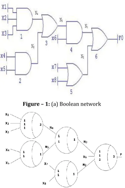
In this section we discuss on simple synthesis procedure using threshold network. The Boolean gate network show in Figure1 (a and b). Which has six gates and four levels. If each Boolean gate are simply replace with a threshold gate, the resulting network will contain five threshold gates and three levels. The network is sub-optimal network due to
node 𝑛1, which is a redundant node. This node can be
replaced with a single threshold gate. Proof of synthesis Boolean function we can written as 𝑓 = 𝑛1 ∨ 𝑛2 can be collapsed to and becomes the 𝑓 = 𝑛3 ⋅ 𝑥6 ∨ 𝑥7 + 𝑥8 now we must determine if a ƒ threshold function is or not. In this case, it turns out that is not a Threshold function. Consequently, we must be split ƒ into smaller nodes using efficient heuristics. We choose to split ƒ as 𝑓 = 𝑛3⋅ 𝑥6 ∨
𝑛2 where 𝑛2= 𝑥7 + 𝑥8 . We can synthesize n3 next. After collapse, a node 𝑛3 = 𝑥1⋅ 𝑥2 ∙ 𝑥3 ∨ 𝑥4∙ 𝑥5. This is not a threshold function. Therefore, we split 𝑥3 into two nodes to get 𝑛3 = 𝑛4 ∨ 𝑛5. Where 𝑛4 = 𝑥1 𝑥2 𝑥3 and 𝑛5 = 𝑛4 𝑥5. These three nodes are threshold functions. The synthesized threshold network is shown in fig. 1(b).It can be seen that the number of gates and levels has been reduced by 30.28% (six to five) and 45% (four to three), respectively. The above example demonstrates that a threshold network synthesis procedure must be address the following key issues
It must be determine the function is threshold logic or not.
If the functions is a not a threshold function it must be able to split on smaller function.
[image:2.595.326.544.93.421.2] The threshold function split using heuristics method If exist redundant node in original Boolean network, it must be those node in the synthesized threshold network.
Figure – 1: (a) Boolean network
Figure – 1:(b) the optimized threshold network
Boolean expressions of given fig (a) is written as 𝑓𝑜 =
(𝑥1 𝑥2 𝑥3 + 𝑥4 𝑥5) ⋅ 𝑥7 (𝑥8 𝑥9), suppose that input of given Boolean expressions is 𝑥1 = 0, 𝑥2 = 0, 𝑥3 = 1, 𝑥4 =
0, 𝑥5 = 0, 𝑥6 = 0, 𝑥7 = 0, 𝑥8= 0, 𝑎𝑛𝑑 𝑥9 = 0, then output of given Boolean expressions’ 0’ similarly the output of the threshold network is written as below in a Table1 1. Table – 1: Synthesize process
INPUT OUTPUT
X1, X2, X3, X4, X5, X6, X7, X8, X9, N5 N4 N3 N2 F
0 0 1 0 0 0 0 0 0 0 0 0 0 0
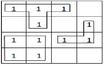
There are many technique are used to determine threshold functions, K-map is one of technique used to determine threshold function. In k-map any non-adjacent, cell, any two adjacent cell and few admissible pattern of three and four cell Threshold functions.
3.1 Admissible Pattern
Admissible pattern is a one of the synthesis or decomposition process to find the non-threshold function two or more factor [14], this apply for every threshold function shown in figure 2. A pattern of
© 2016, IRJET ISO 9001:2008 Certified Journal
Page 1377
[image:3.595.63.262.140.267.2] Any admissible pattern for functions of three variables is also an admissible pattern for functions of four or more variables, and so on.
Figure -2: Admissible pattern network
in this analogously to the synthesis of AND–OR networks, a threshold-logic realization of an arbitrary switching function, can now be achieved by selecting a minimal number of admissible patterns such that each 1-cell of the map is covered by at least one admissible pattern. Generally a threshold logic network is synthesize by a simple linear programing based approach. Together weight and threshold of any function generally consider only positive value [15], and most important irredundant target wire is removal by adding to the new threshold logic gate at other positions
Step-1 firstly apply the multiple number of input to the threshold network. All inputs are like that 𝑥1, 𝑥2,⋅⋅⋅⋅⋅⋅, 𝑥𝑛. Step-2 grouping and decompositions of a threshold network.
Separate the input whose weight is equal to the threshold value of the objective gate as a single group.
Separate the rest of inputs are another group of this threshold network.
Each group is decompose to the equal weight in a threshold network.
There are several types of grouping and single grouping and multiple type of grouping [16].
Single grouping: - in a single grouping if input is giving to the threshold gate 𝑥𝑖 and cross ponding to the weight 𝑊𝑖 sum is satisfied the following equation that is 𝑥𝑖 = 𝑤𝑖 < 𝑇.
If the threshold network is some weight are unequal and some are identical then the given system is fragmented in to two network as this whole process are called decomposition grouping figure 3. And figure 4. Show that the decomposition of network.
[image:3.595.325.546.368.524.2]Figure – 3:Threshold gate network.
Figure – 4:Decomposition threshold gate.
Step-3 removal of redundant wire which is not required to the threshold network, there are given a two possible result, first is simple threshold logic gate and useless threshold logic gate input.
Useless input: - if the input is useless if and only if the output of this LTG (linear threshold gate) is intact when this input toggles under all input combinations. Or another way to define a useless threshold gate suppose all weight are less than threshold level then output of threshold gate is always zero or one in all input combination. Step-4 if the redundant wire is not critical the remaining threshold gate is not useless.
© 2016, IRJET ISO 9001:2008 Certified Journal
Page 1378
Analyses the functionality inputs of an LTG with critical-effect paths for the construction of rectification network. Go to the synthesis process. Step-5 if the redundant wire is critical father simplified the weight sum constraint. If it is not rectified the weight sum then change the threshold value after that simplified the AND threshold network
STEP-6 after that process of all steps then threshold network is synthesize.
4. REALIZATION OF SEVERAL TYPE THRESHOLD
GATE LOGIC STYLE
4.1 Capacitive Threshold-Logic Gate
A capacitive threshold gate dense and fast threshold-logic gate with a very high fan-in capacity is described [17]. The Boolean function performed by the gate is soft programmable. This is accomplished by adjusting the threshold with a dc voltage. However, the gate can evaluate multiple input vectors in between two successive reset phases because evaluation is non-destructive. Asynchronous operation is, therefore, possible. The gate operates in a two-phase no overlapping clock scheme comprising a reset phase defined by the clock 𝜙𝑅 and an evaluation phase defined by 𝜙𝐸. In a reset phase, the row voltage 𝑉𝑅, is reset to the logic threshold voltage Vth of the inverter stage of the comparator, while the capacitor bottom plates are Precharge to a reference voltage Vref. The changing of the comparator is indifferent at the end
of 𝜙𝑅. This leaves the row of capacitor upper plates
[image:4.595.325.543.80.263.2]practically floating until the arrival of next phase. Throughout this time, only the leakage current of the comparator is to reset due to charge alter established on the row during 𝜙𝑅. Evaluation phase begins with the arrival of 𝜙𝐸. Binary input signals, 𝑉𝑖, 𝑉𝑗 𝑎𝑛𝑑 𝑉𝑀 are forced onto the columns, and consequently, row voltage is perturbed from the reset level Vth. Ignoring show in the figure 5. The gate can be used synchronously or asynchronously, but it also needs to be periodically reset. However, this capacitive threshold gate frequency mode operation is very low even in the case of a very large fan-in.
Figure – 5: a capacitive threshold gate
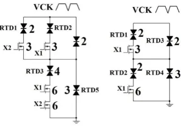
4.2 A XOR Threshold Logic Implementation
through Resonant Tunneling Diode
This XOR gate tunneling diodes (TDs) have been used in widely applications like in achieving very high speed in wide-band devices and circuits that are beyond conventional transistor technology. RTD works on concept of multi threshold logic [18] and MOBILE where MOBILE is monostable bistable logic element. MOBILE is series connection of two RTDs which contain load RTD and driver RTD. Whenever MOBILE have load RTD than positive weighted inputs are connect to parallel with load RTD and negative weighted inputs are connect parallel with driver RTD, the driver RTD and load RTD is works according to bias voltage (Vbias) and gives output as Vout. Equivalent circuit of XOR make using RTD and threshold logic and simulate it using HSPICE. The RTD areas should be adjusted to appropriate values for correct operation, moreover, the transistors width may be tuned for better performance in the MOBILE-based circuits shown in the figure 6. [19].
[image:4.595.333.516.529.656.2]© 2016, IRJET ISO 9001:2008 Certified Journal
Page 1379
The design of XOR gates of different structures werepresented in literature over the years. Most of XOR gate circuits are design based on FET and CMOS transistors [20]. At some point, the voltage drop across the RTD will increase such that it is operating in the NDR region (i.e., the dynamic resistance will increase), and the input current will drop sharply, turning off the transistor, thus switching At some point, the voltage drop across the RTD will increase such that it is operating in the NDR region (i.e., the dynamic resistance will Increase), and the input current will drop sharply, turning off the transistor, thus switching Vout back to Vbias. Whenever we apply the bias voltage, current is increases at certain point, after that current is decreases at certain point and then current is increases, so that have two stable point and minimize the power dissipation than CMOS.
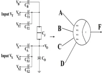
4.3 A SET Linear Threshold Gate
This type of threshold gate is work on single electronics transistor (SET) [21]. A Single electron transistor it is electronics device which is works on tunneling phenomena. In this implementation of TG is replacing as single electron transistor which is works like threshold gate shown in fig.7. Working of linear threshold gate , TG it is a device which are able to compute the Boolean function it given that threshold gate, TG it is a device which are able to compute the Boolean function it given that [22],
𝑓 (𝑥1, 𝑥2,∙∙∙∙∙∙∙∙∙∙∙∙, 𝑥𝑛 ) = {
1, 𝑖𝑓 ∑ 𝑤𝑖 𝑛
𝑖=1 𝑥𝑖 ≥ 𝑇
0, 𝑖𝑓 ∑ 𝑤𝑖 𝑛
𝑖=1 𝑥𝑖 < 𝑇
[image:5.595.69.248.570.697.2]Where 𝑥𝑖 is then Boolean inputs and 𝑊𝑖 are the corresponding n integer weights. The linear threshold gate performs a comparison between the weighted sum of the inputs and the threshold value T. If the weighted sum of inputs is greater than or equal to the threshold, the gate logic 1. Otherwise, the output is logic 0.
Figure – 7: SET based threshold gate
LTG circuits are work on the basis of tunneling phenomena and critical voltage.
If the critical voltages 𝑉𝐶 are tunneling and which also act as the intrinsic threshold level. If the voltage across the junction is larger than 𝑉𝐶 an electron will tunnel through the junction in the opposite direction, resulting output is logic 1.The biasing voltage 𝑉𝐵, weighted by the capacitor 𝐶𝐵, is used to adjust the gate threshold to the desired value T. The input signal 𝑉𝑇 and cross pounding weight sum 𝐶𝑇 is added to the voltage across the tunnel junction and another input signal 𝑉𝑋 and crosses pounding weight sum 𝐶𝑋 subtract from the voltage across tunnel junction as Fig. 2. Using this approach, we can design a threshold gate [23].
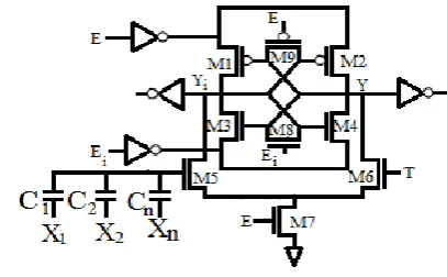
4.4. Charge Recycling CMOS Threshold Logic Gate
A new implementation of a threshold gate based on using charge recycle technique. It is design by positive weights sum and threshold level. In this circuit the output 𝑌 and its complement 𝑌𝑖 generates by using cross coupled 𝑀1 and 𝑀4 transistor. Precharge and evaluate is specified by the dual enable clock signals 𝐸 and its complement 𝐸𝑖. The inputs 𝑋𝑖 are capactively coupled onto the floating gate 𝜙 of 𝑀5, and the threshold is set by the gate voltage T of 𝑀6 transistor. The potential 𝜙 is given by where Ctotal is the sum of all capacitances, including parasitic, at the floating node. Weight values are thus realized by setting capacitors 𝐶𝑛 to appropriate values. The enable signal 𝐸 controls the Precharge and activation of the sense circuit. Transistors𝑀8 and 𝑀9 equalize the outputs. The logic gate has two
phases of operation, the evaluate phase and the equalized phase. When 𝐸𝑖 is high the output voltages are equalized. When 𝐸 is high, the outputs are disconnected and the differential circuit (𝑀5 - 𝑀7) draws different currents from the formerly equalized nodes 𝑌 and 𝑌𝑖.The transition. In this way the circuit structure evaluates it' the Weighted sum of the inputs, 𝜙 is greater or less than the threshold T, and a TL gate is realized shown in the fig.8. [24].
Advantage of this circuit very low power dissipation and high operating speed, as well as high strength under process, temperature and supply voltage variations, and is therefore highly appropriate used as an element in digital integrated circuit implementation.
© 2016, IRJET ISO 9001:2008 Certified Journal
Page 1380
Figure -8: Charge recycling CMOS threshold logic gate4.5. Memristor Threshold Logic
[image:6.595.55.271.409.505.2]In this threshold gate implemented by using memristive devices threshold logic and CMOS threshold logic. Using both two logic that is implemented by threshold gate function by using ratioed diode-resistor logic (RDRL) show in fig.9. [25]. A memristive device works on meanly voltage or current operations depending on electrodes changes the resistivity (“memory state”) of the thin film material shown in the fig.10. The memory state of properly engineered devices is non-volatile and could be read without disturbing it with a smaller electrical stress capability, [26].
[image:6.595.307.538.414.522.2]Figure- 9: Memristive Threshold Logic
Figure -10: I−V characteristics of memristive devices Working of memristive devices threshold logic gate which is comprised of several (N) memristive devices connected in parallel to a single pull-down resistor RL. To suppress leakage currents between inputs of the gate, operating voltage is chosen from the different condition.
𝑉𝑡ℎ < 𝑉𝑑𝑑 < 2𝑉𝑡ℎ (3)
Ignoring leakage currents below VTH, i.e., currents via ROFF resistance fig.10 the output voltage of ratioed DRL always ranges from 0 to VDD−VTH and is equal half of that value when
∑ 𝑥𝑖 𝑅1
𝑖
𝑁
𝑖=1 = 𝑅1𝐿 (4) When DRL is connected to a CMOS gate so that is called voltage swing is restored and the output of the CMOS gate is used to drive the inputs of other logic gates. We chose D-flip-flop because of it’s a high efficiency and high-throughput pipelined circuits [27]. Assuming that the CMOS gate is designed to restore a signal to VDD (logical “1”), if the input voltage is larger than (VDD–VTH)/2 and otherwise to 0 (logical “0”), using these two circuits implements a LTG. Where 𝑊𝑖= 𝑅1
𝑖 and 𝑇𝐿=
1
𝑅𝐿. Note that the no integer (rational) weights and the threshold could always be converted to the integer numbers required by the original definition of LTG by multiplying both sides of the inequality in (1) by the appropriate constants [28].
Table- 2: Performance of Threshold Gate
TG logic style Frequency Technology (nm)
CTG 30 MHz 120 RTD 215 GHz 250 SET - - CRTG 200 MHz 200
MTG 300MHz 180
3. CONCLUSIONS
The performance analysis of realization process of different types of threshold gate shown in above figure. The performance of several threshold gate depending on implementation technique of threshold gate with different threshold voltage, frequency and temperature variations. A comparison with other TL realizations shows that this threshold gate has very low power dissipation. Therefore threshold gate highly used in digital integrated circuit implementation.
ACKNOWLEDGEMENT
The authors would like to thanks prof. Dr. C.T.Bhunia Department of ECE supported by National Institute of Technology Arunachala Pradesh India.
REFERENCES
[image:6.595.60.262.462.654.2]© 2016, IRJET ISO 9001:2008 Certified Journal
Page 1381
[2] S. Roy and C. T. Bhunia (2014), “Minimizationalgorithm for multiple input to two input variables,” in Proc. Int. Conference on Control, Instrumentation Energy and Communication, (CIEC14), IEEE, pp. 555-557.
[3] Robert O. Winder (19610, “Single stage threshold logic. In Proceedings of the 2nd. Annual Symposium on Switching Circuit Theory and Logical Design, (SWCT1961), PP.321-332.
[4] Goldmann Mikael, et al., (1992) “Majority gates vs. general weighted threshold gates”, Computational Complexity vol. 2, pp. 277-300.
[5] R. Zimmermann and W. Fichtner (1997), “Low-power logic styles: CMOS versus Pass-Transistor Logic,” IEEE J. Solid-State Circuit, Vol. 32, PP. 1079-1090.
[6] Auer, U., et al., (2000) “Threshold Logic Circuit Design of Parallel Adders Using Resonant Tunneling Devices”, IEEE transactions on, vol. 8, no. 5, pp. 558-572. [7] A. P. James (2014), "Threshnomics: An Introduction to
Threshold Logic in Algorithms and Circuits." Journal of Computer Science & Systems Biology, vol. 7, pp. 235-240.
[8] Koichi, M., et al., (1998), “High-speed and low-power operation of a resonant tunneling logic gate MOBILE”, Electron Device Letters, IEEE, vol. 19, no. 3, pp. 80-82. [9] Leblebici, Y., et al., (1996), “A compact high-speed (31, 5) parallel counter circuit based on capacitive threshold-logic gates”, Solid-State Circuits, IEEE Journal, vol. 31, no. 8, pp. 1177-1183.
[10] Marius, P., et al., (2003), “Cmos implementation of generalized threshold functions.” In Artificial neural nets problem solving methods, Springer Berlin Heidelberg, pp. 65-72.
[11] Casper, L., et al., (2002), “A full adder implementation using SET based linear threshold gates”, In Electronics, Circuits and Systems, 9th IEE International Conference on, vol. 2, pp. 665-668.
[12] M. J. Avedillo and J. M. Quintana (2004), “A threshold logic synthesis tool for RTD circuits, “In Digital System Design, IEEE Euromicro Symposium on, pp. 624-627. [13] Judge, et al., (1998), “Introduction to the theory and
practice of econometrics”, (1988).
[14] Mazzarella and G. Panariello (1993), “Pattern synthesis of conformal arrays”, In Antennas and Propagation Society International Symposium, AP-S. IEEE Digest, pp. 1054-1057.
[15] Michiel, L., et al., (200), “Asynchronous design using commercial HDL synthesis tools”, In Advanced Research in Asynchronous Circuits and Systems, IEEE Proceedings. Sixth International Symposium on, pp. 114-125.
[16] J. B. Shyu., et al., (1984), “Random error effects in matched MOS capacitors and current sources,” IEEE J. Solid-State Circuits, vol. SC-19, pp. 948-955.
[17] Hakan, O., et al., (1996), “A capacitive threshold-logic gate”, Solid-State Circuits, IEEE Journal, vol. 31, no. 8, pp. 1141-1150.
[18] D. R. Haring, “Multi-Threshold Threshold Elements,” IEEE Trans. on Electronic Computers, Vol. 15, pp. 45-65, February 1966.
[19] D. N. Kumar, and V. Kumari (2012), “A XOR threshold logic implementation through resonant tunneling
diode”, International Journal of VLSI Design & Communication Systems, vol. 3, no. 5, pp. 137-147. [20] P. Sun, and G. Haddad (1998), “Resonant Tunneling
Diodes: Models and Properties,” IEEE journal, vol. 86, pp. 641-660.
[21] A. N. Korotkov (1999), “Single-Electron Logic and Memory Devices,” international Journal of Electronics, vol. 86, pp. 511-547.
[22] Raushan, K., et al., (2016), “Study of Threshold Gate and CMOS Logic Style Based Full Adders Circuits”, 3rd IEEE international Conference on electronics and communication systems (ICECS), pp. 173-179.
[23] Pinaki, M., et al., (1998), “Digital Circuit Applications of Resonant Tunneling Devices,” Proceedings of the IEEE, Vol. 86, no.4.
[24] Celinski, P., et al., (2001), “Low power, high speed, charge recycling CMOS threshold logic gate,” Electronics Letters, vol. 37, no. 17, pp. 248-249. [25] Sangho, S., et al., (2011), “Memristor applications for
programmable analog ICs,” IEEE Trans.Nanotechnol., vol. 10, no. 2, pp. 266–274.
[26] Kamran, E., et al., (2012), “Memristive device fundamentals and modeling: Applications to circuits and systems simulation,” Proc. IEEE, vol. 100, no. 6, pp. 1991–2007.
[27] Marius, P., et al., (2003), “Design and experimental results of a CMOS flip-flop featuring embedded threshold logic,” in Proc. ISCAS, Bangkok, Thailand, vol. 5, pp. 253–256.
[28] Bia-sun, K., et al., (1999), “Asynchronous sensc differential logic,” Dig. Tech. Pup. IEEE Int. Solid-Siate Circuils, pp. 284-285.
Raushan Kumar, is presently pursuing his M. Tech. studies in the Department of Electronics and Communication Engg. National Institute of Technology Arunachala Pradesh India, he received his B.Tech Institute of Electronics and Telecommunication Engineering (IETE) New Delhi (India)-2013. His area of interest is CMOS, VLSI Technology and FPGA.
Prashant Kumar received the B.Tech. Degree from Bundelkhand University, Jhansi, India in 2013, in Instrumentation Engineering. Currently, he is pursuing in M.Tech in Electronics Design & Manufacturing from National Institute of Technology, Arunachal Pradesh, India. Research interests: Control System, VLSI Design, Power Electronics.
© 2016, IRJET ISO 9001:2008 Certified Journal