International Journal of Emerging Technology and Advanced Engineering
Website: www.ijetae.com (ISSN 2250-2459, ISO 9001:2008 Certified Journal, Volume 4, Issue 1, January 2014)
Clock Domain Crossing Verification in a System on Chip
Kamal prakash pandey
1, Rakesh Kumar Singh
2, Surendra Kumar Tadi
31,2Associate Professor Department of Electronics & Communication Engineering SIET, Allahabad, India 3Research Scholar Electronics & Communication Engineering SIET, Allahabad, India
Abstract— A Modern complex SOC has a number of
different asynchronous clock domains and data is frequently transferred from one clock domain to another which needs to be synchronized. Designer uses many types of synchronizer, most commonly used synchronizer is 2 flop synchronizer which is mainly used for control signals, there are other types of synchronizer such as MUX synchronizer, FIFO synchronizer, these are used when a multi bit signal or a bus needs to be synchronized in destination domain. Due to large design size and presence of multiple asynchronous clocks in a SOC, synchronizer is needed at thousands of places and it becomes very important to ensure if proper synchronization is done at all required places. STA does not cover clock domain crossing paths while gate level simulation’s are very limited since it does not cover all the CDC paths, it flags violation on CDC path only if timing’s are not met. As a standard practice, CDC verification for a SOC is mostly done using formal tools such as ―lec –verify‖, Questa CDC solution etc. These tools perform structural CDC checks for a given design.
This paper explains about clock domain crossing requirement, synchronizer structure and a methodology to find out various issues in structural CDC checks. It also explains about reset synchronizer requirement & its verification.
Keywords-- CDC, Clock domain crossing verification, Synchronizers,Gate level simulation.
I.INTRODUCTION
Data transfers between different clock domains require synchronization. Failing to synchronize data and control transfers between asynchronous clock domains can lead to setup and hold violation of flip-flops. These timing violations may cause signals to go metastable; they also may cause functional errors in the design.
Chip failures due to incorrect synchronization are very difficult to detect, and manifest themselves as seemingly random errors and lockups of the design. For an error to show up, the right combination of clock edges and data needs to occur. Detecting these problems before fabrication can also be difficult, since RTL simulation is typically done without detailed timing information; again, even with detailed timing information, the right combination of clock edges and data need to occur in order to detect any problems.
To address clock domain problems due to metastability and data sampling issues, designers typically employ several types of synchronizers. The most commonly used synchronizer is based on the well-known two-flip-flop circuit.
It turns out, however, that this is a very sensitive circuit, and all too often it is designed incorrectly, resulting in intermittent (and elusive) synchronization failures. Other types of synchronizers are based on handshaking protocols or FIFOs. In a limited number of cases it may be useful to employ dual-clock FIFO buffers or other mechanisms optimized for domains with same or similar clock frequencies.
To accurately verify clock domain crossings, structural clock domain analyses should be carried out. Structural clock domain analysis looks for issues like multi-domain combinational logic, insufficient synchronization, or combinational logic driving flip-flop-based synchronizers.
II.WHY SYNCHRONIZERS REQUIRED
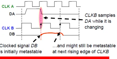
[image:1.595.328.555.484.566.2]As shown in the Figure 1, there is a possibility that data input is changing during the time positive edge of the clock appears, as a result setup-hold time violation can occur and output may go into metastable state as shown in Figure 2, and this may cause functional failures in the design.
Figure 1: Flop FB capturing DA coming from a different clock domain
[image:1.595.332.559.605.720.2]International Journal of Emerging Technology and Advanced Engineering
Website: www.ijetae.com (ISSN 2250-2459, ISO 9001:2008 Certified Journal, Volume 4, Issue 1, January 2014)
[image:2.595.62.266.184.412.2] [image:2.595.63.263.189.274.2]618 Figure 3 shows design of a 2-flop synchronizer where additional flop gives metastable signal time to become stable as shown in Figure 4.
Figure 3: 2 flip flop synchronizer circuit
Figure 4: Metastability is resolved at FB2
III. STRUCTURAL CLOCK DOMAIN VERIFICATION.
Structural analysis looks at the connectivity and logic of the design to find problems. The process typically starts with the clock tree being identified; the master clocks may be either specified manually, or automatically detected. Once the clock tree and the clock domain associations have been analyzed, structural analysis algorithms identify issues such as:
1) Unresolved clocks – An unresolved clock is one that can not be related back to single master clock. This may happen because signals unexpectedly used as clocks. Another source of unresolved clocks would be derived clocks that come from multiple master clocks, due to clock muxing. 2) Multi-domain combinational logic.
3) Use of insufficiently synchronized signals from flip-flop based synchronizers, For instance, if the designer specified that three flip-flops are required for synchronization, all one-and two-flop synchronizers are flagged.
4) Clock domain crossing that does not use synchronizers.
5) Primary outputs driven from insufficiently synchronized signals from flip-flop based synchronizers.
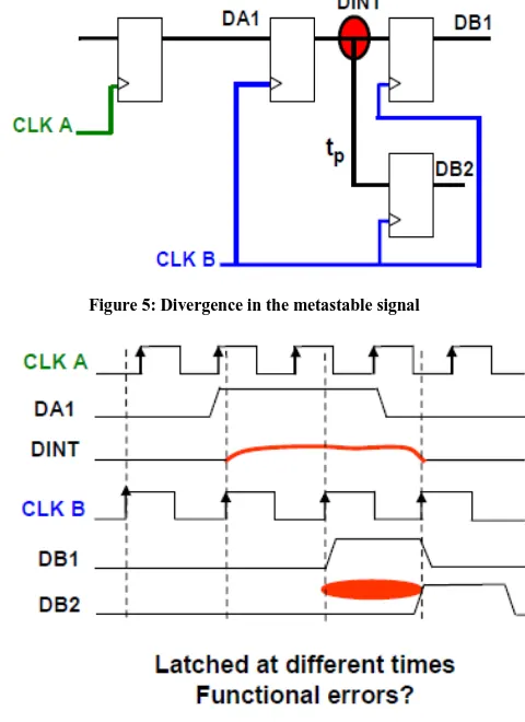
3.1 Structural CDC: Multi fan out issues
[image:2.595.315.555.257.587.2]A divergence in the metastable signal can cause functional errors as seen in the Figure 5, DB1 and DB2 came out at two different clock edges as the settling and latching values of these metastable signals to the two flops are at the different times.
Figure 5: Divergence in the metastable signal
Figure 6: Mismatched DB1 and DB2 timings
A divergent logic style to multiple synchronization paths runs the risk of causing functional errors. As
[image:2.595.58.268.298.409.2]International Journal of Emerging Technology and Advanced Engineering
[image:3.595.322.562.142.356.2]Website: www.ijetae.com (ISSN 2250-2459, ISO 9001:2008 Certified Journal, Volume 4, Issue 1, January 2014)
[image:3.595.318.566.547.737.2]Figure 7: Divergence in the crossover path
Figure 8: Improper DB1 and DB2 timings
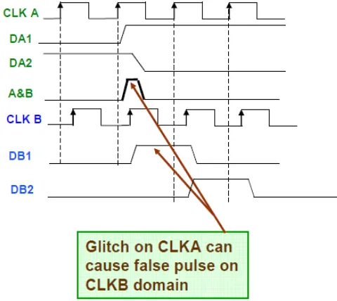
3.2 Structural CDC: Glitch issues
Combinational logic driving flip-flop based synchronizers. Glitches and hazards generated by such logic may be caught by the receiving clock domain and cause elusive intermittent failure. Clock domain crossover paths are false paths for timing tools; any logic in this path must be carefully crafted and verified, because the logic can cause glitch and create functional errors downstream. In Figure 9, although the two source flops give the pulse at the same time, the propagation delay (Td) in post-layout masks creates the pulse as shown in Figure 10, because it is a false path (ignored by the timing tool), the design techniques should consider these occurrences.
Figure 10: Spurious glitch captured by destination clock domain
3.3 Structural CDC: Reconvergence issues
Once synchronization is completed, the structures beyond the synchronizers still matter. The design must ensure that the synchronized signals do not converge— reconvergence can create functional errors. As shown in Figure 11, signal DB2 is synchronized from DA2 and DB4 is synchronized from DA4, there can always be one clock cycle discrepancy in sampling signal from a different clock domain, it might happen that DB4 is available one cycle later than DB2 or vice versa. This can
cause functional issue in reconvergence requires
asynchronous reset to be synchronized in the destination clock domain before connecting at the flop logic.
[image:3.595.57.273.639.762.2]International Journal of Emerging Technology and Advanced Engineering
Website: www.ijetae.com (ISSN 2250-2459, ISO 9001:2008 Certified Journal, Volume 4, Issue 1, January 2014)
620 One major source of false errors in structural analysis is due to signals that are static, and are not synchronized between clock domains. Examples would be BIST enables or clock select pins. Typically these signals are set when the design comes up, and do not change in normal operation.
Even if static signals are defined as such, it may not be sufficient for this to remove all the false errors in the report. For example, if there is a multiplexer with inputs from different domains. If the mux select defined to be a static signal, the mux output will definitely be in one domain, but without more information it is not possible to determine which domain. In many cases static signals will have to be declared along with values, essentially putting the chip in a particular mode in which to do clock analysis.
Other types of structural clock domain analysis checks analyze specific synchronizer types. Multi-flop synchronizers are typically used to synchronize single-bit signals. The problem with using multi-flop synchronizers on data signals is that if more than one bit changes at a time, due to different delays and skews on the individual synchronizers, one bit of the data may be sampled at a different time than others. This could lead to incorrect data being transferred across domains. One method to avoid this issue is to gray-encode the data such that only one bit changes at a time.
Other methods are to use synchronizers designed to transfer data signals. One of these types of synchronizers commonly used is handshake-based.
IV. SET/RESET SYNCHRONIZATION
[image:4.595.332.564.143.297.2]As shown in the Figure 12, when reset is removed or deasserted asynchronously with respect to clock, it can cause metastabilty in the design. Also due to different path delay in the reset, different flops might be resetted in different clock cycles; this can lead to functional errors in the design. This.
Figure 12: Metastability during reset deassertion
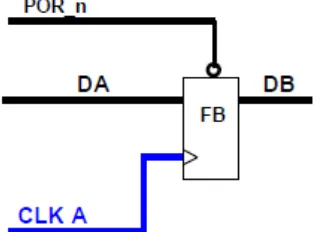
The CDC asynchronous set/reset synchronizer check verifies that DFFs in the design are synchronized properly during deassertion of set/reset. If a DFF has an asynchronous set or reset, care should be taken to ensure that it is deasserted synchronously. If the deassert of set/reset happens close to the active edge of the clock and the data input changes violating the setup-time window or hold-time window, then the DFF could go into a metastable state.
[image:4.595.89.249.588.704.2]Asynchronous assertion does not cause metastability because the clock is bypassed. A well-known technique to solve this issue is to connect the reset of the DFF to a series of synchronized DFFs that has a tied data input and the same set/reset as the original DFF. This is shown in the following Figure 13.
Figure 13: synchronizing reset signal
V. STRUCTURAL CDC VERIFICATION SOLUTION
International Journal of Emerging Technology and Advanced Engineering
Website: www.ijetae.com (ISSN 2250-2459, ISO 9001:2008 Certified Journal, Volume 4, Issue 1, January 2014)
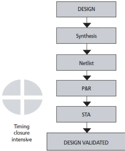
[image:5.595.57.276.216.480.2]In the ―timing-closure–only methodology‖ (see Figure 13), these errors are can be checked during the end stages of the design cycle, i.e., in the gate simulation with SDF back annotation which has many limitations. Structural verification of CDC adds a great deal of value in unearthing all CDC synchronization issues.
Figure 14: Timing closure only methodology
Figure 15: Methodology with CDC verification
4.1 Clock Domain Partitioning
The major step in the setup for a CDC check is the proper partitioning of designs into asynchronous domains. Propagation and extraction techniques can aid the user in partitioning.
Propagation is the forward flow of the user-defined clock attributes through different design structures. The user can control the forward propagation. Extraction builds the domain partition by starting from the clock pin of each flop and creating different clock trees.
[image:5.595.324.554.302.452.2]As shown in the Figure 15, after reading design, top level CLK_A and CLK_B is defined, pll/clk_out is also defined at a particular hierarchy, design flops can be optionally initialized using a vcd or sequence, constraints from STA or clock mux select can be added & required clock domain rule is defined. Once ―set system mode verify‖ is done, clock domain for each and every flop is determined, error is issued for incorrect or incompletely specified clock domains.
Figure 15: Example do file from Cadence LEC –verify
Because the possibility exists that more domains could be created than the designer envisioned, a utility should be provided to associate clocks and data pins and ports. The clock domain partitions also depend on constraints in the design for the correct flow of the paths, so there should be a way to constrain the design and declare static signals. Configuration register information should be used in conjunction with the utilities to correctly define the clock domain partitions.
4.2 CDC path rules and validation
Once the clock domains are properly identified, the CDC paths become apparent. A rule-based technique can then be used and applied to the CDC paths. The rules can specify the synchronization scheme (flop or MUX), the allowable structures in the crossover path and the paths in the synchronizer. Tools can provide either global or local rules.
[image:5.595.50.284.517.679.2]International Journal of Emerging Technology and Advanced Engineering
Website: www.ijetae.com (ISSN 2250-2459, ISO 9001:2008 Certified Journal, Volume 4, Issue 1, January 2014)
622 The reconvergence of CDC signals should be applied only to the flop-based synchronizers, and analysis should start after the specified flop rule. A rule R1 may specify a three-flop synchronizer from CLK 1 to CLK 2; and another rule (for example, R2) may specify a two-flop synchronizer from CLK 3 to CLK 2. The reconvergence check should start analysis after three flops to data paths from CLK 1 to CLK 2 and two flops to data paths from CLK 3 to CLK 2, and see if the two CDC paths converge. Once the structural analysis has been completed, the formal analysis and techniques can be used to verify the stability of all the signals in the CDC path. This formal analysis checks that the hold logic and the latching logic have correct functionality. For vectors that are flop-synchronized, formal analysis can be Used to create a property to ensure that the vector is Gray-encoded.
VI.CONCLUSION
With a growing number of clocks in today’s SoC designs, increased design complexity, and pressure for first silicon success, all clock and timing issues have become a verification challenge. Existing methods provide an ad hoc partial verification that is time consuming and error prone. Automatic formal verification techniques are needed to ensure that multiclock designs are correct prior to tape out.
The solution must also prevent sources of failures in multiclock designs, such as metastability. A clock domain crossing (CDC) verification solution must address this verification challenge, while maximizing overall productivity and effectiveness.
It needs to cover clock domain analysis and structural and functional verification, addressing both RTL and gate-level verification needs.
VII. ACRONYMS USED
GLS : Gate level simulation CDC ― Clock Domain Crossing STA : Static Timing analysis DFT : Design for Test SoC : System on chip SDF : Standard Delay Format VCD : Value change dump RTL : Register Transfer level BCS : Best Case Simulation WCS : Worst case simulation LEC : Logic Equivalence check IP : Intellectual Property
REFERENCES
[1] Cummings, Clifford E. Synthesis and Scripting Techniques for
Designing Multi-Asynchronous Clock Designs. SNUG 2001.
[2] Wakerly, John. Digital Design Principles and Practices. Prentice
Hall, 2000.
[3] The Need for an Automated Clock Domain Crossing Verification
Solution, Mentor Graphics Corporation. www.mentor.com/fv
[4] Clock Domain Crossing (CDC) Design & Verification
Techniques Using SystemVerilog Clifford E. Cummings Sunburst Design, Inc. [email protected]
[5] Critical clock-domain crossing bugs by shaker Sarwary and
Saurabh Verma • Atrenta Inc
[6] Challenges in Verification of Clock Domain Crossings by Vishnu