2019 International Conference on Computation and Information Science (ICCIS 2019) ISBN: 978-1-60595-644-2
Design and Implementation of High Precision
DACs Calibration Algorithms Based on FPGA
Guosheng Peng, Yufeng Chen, Zhengtao Xiang, Kai Che
and Zesheng Fang
ABSTRACT
High-precision DACs are widely used in various fields, and the error of DAC chips has always been a key factor affecting digital-to-analog conversion. DACs calibration algorithms have become an important research hotspot. In this paper, we design a high-precision DACs calibration system based on FPGA, analyze the calibration principle and error of high-precision DAC chips, and propose three kinds of DACs calibration algorithms and verify the analyses. The optimized algorithm can effectively eliminate the system's offset error, gain error, process defect error, etc. The system's comprehensive performance and output accuracy are improved, and the precise control of digital-to-analog conversion is realized.
1. INTRODUCTION
Digital-to-Analog Converter (DAC) is a necessary device for the interface between digital circuit and analog circuit [1]. Along with the rapid development of electronic technology, traditional analog signals cannot satisfy the current practical application requirements. Large-scale processors such as DSP, FPGA and CPU process digital signals, so we need to convert the processed digital signals into analog signals through DACs. High-precision DACs are mainly used in industrial process control, measurement and analysis. There are different requirements for the performance of DACs in different fields. Calibration techniques for DACs have long been one of the important factors affecting accuracy.
Since the process, noise, and reference voltage fluctuations all cause errors in the DACs, the system cannot be controlled very accurately in applications. Foreground calibration is used for DAC calibration by calibrating the accuracy of the DAC chip in hardware design [2]. The potentiometer calibration method calibrates the offset error
and gain error of DACs by adjusting the potential [3]. In this paper, three methods are used to calibrate the DACs through the FPGA. The first is the look-up table method for forced calibration of the data; the second is to use two points to process the original data line for calibration purposes; the third is adaptive calibration, which can be automatically calibrated at any time and is suitable for complex environment.
2. SYSTEM AND ERROR
2.1 High Precision DACs Calibration System Based on FPGA
The system chip uses a 16-bit serial DAC chip,the calibration control of which is implemented by the FPGA. The system mainly consists of three modules, which are serial port receiving [4], data correction and DAC control. Firstly, 16-bit data is sent to the calibration system through the serial port, and then the data is imported into the calibration module for comparison analysis. Finally, the corrected data is input to the DAC chip to realize precise control of the digital-to-analog conversion.
2.2 Characteristics of DACs Chip Error
The characteristics of DACs chip error must be analyzed before discussing the calibration algorithms. First consider total unadjusted error (TUE):
TUE = √𝑂𝑓𝑓𝑠𝑒𝑡𝑒𝑟𝑟𝑜𝑟2+ 𝐺𝑎𝑖𝑛𝑒𝑟𝑟𝑜𝑟2+ 𝐼𝑁𝐿𝑒𝑟𝑟𝑜𝑟2 (1)
The offseterror [5] represents the difference between the actual and ideal output voltage when the DAC input is 0x00. The gainerror[6] represents the difference between the actual and ideal slope of the DAC.Integral Nonlinearity (INL)[7] and Differential Nonlinearity(DNL)[8] of DACs are important parameters used to describe the static transmission characteristics of DACs. DNL is the adjacent level difference measured over the vertical span, which is the maximum deviation between the two adjacent DACs outputs and the ideal 1 LSB. INL is the maximum difference between the actual and the ideal finite precision in the vertical direction.
3. ANALYSIS OF DACs CORRECTION ALGORITHMS
As mentioned above, for the DAC chips, the errors that can be corrected are the offset error and the gain error. The specific calibration algorithms are as follows.
3.1 Contrast Calibration of Lookup Table Method
method is to map the theoretical value and the measured value, and the original actual measured value is associated with the theoretical value to achieve the same actual value of the output as the theoretical value. The key point of this method is the establishment of the LUT, which needs to accurately measure the corresponding data of a large number of input digital and output voltage values in order to establish an accurate LUT. In the process of contrast calibration of LUT, the data can be stored by partition, which can effectively reduce the comparison time when comparing data, so as to improve system efficiency and reduce resource consumption.
3.2 Calibration of Two-Point Method
The calibration of two-point method takes a point at each end of the linear region of the DACs, measures the actual voltage at two points, calculates the difference between the actual and the theoretical voltage, and obtains the gain calibration ratio by the slope of the two points, and finally gets the adjusted code. It is worth noting that this method can handle outputs that are outside the control range of the DAC linear region. The theoretical process is as follows:The slope of the actual curve m:
m =
𝑦2−𝑦1𝑥2−𝑥1 (2)
Where x1 and x2 represent the two-point input code, and y1 and y2 represent the corresponding output voltages.
The gain error is:
* 2
[% ] ( 1) *100
n
REF
m
GainError FSR
V
(3)
Where 𝑉𝑅𝐸𝐹 is the reference voltage and n is the number of DAC valid data bits. The average gain rate is:
GainCalRatio =
11+𝐺𝑎𝑖𝑛𝐸𝑟𝑟𝑜𝑟100 (4)
The offset error is:
1 1 [ ]
OffsetError V y x m
(5)
The average offset code is:
OffsetCalCode = −GainCalRatio ∗𝑂𝑓𝑓𝑠𝑒𝑡𝐸𝑟𝑟𝑜𝑟∗2𝑉 𝑛
𝑅𝐸𝐹 (6)
The adjusted code is:
The essence of the algorithm is to eliminate the offset error and gain error, reduce the TUE, and achieve the purpose of calibration. Ideally, the calibrated TUE is:
TUE = √𝐼𝑁𝐿𝑒𝑟𝑟𝑜𝑟2 (8)
3.3 Calibration of Adaptive Method
The adaptive calibration method adds an adaptive calibration function based on the two-point calibration method, which enables calibration of the DACs system at any time. Since the conversion accuracy of the DACs system is affected by the reference voltage and external environmental factors such as temperature, the output of the system will drift as the system runs. In order to ensure the high precision of the system, the two-point calibration can be automatically realized by FPGA at the initial time of system power-on. It can also be set to realize the system adaptive calibration for a period of time. At the same time, the DACs system can be calibrated at any time through external button.
4. EXPERIMENT ANALYSIS AND RESULTS
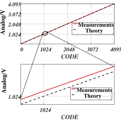
In order to verify the above algorithm, the DAC chip TLV5618 is analyzed in detail. Before starting the verification, all the digital quantities of the chip and the corresponding actual analog output voltage values are first measured and recorded. All the recorded values are plotted by MATLAB, and the section in the figure is enlarged(Fig. 1). We can see that the measured value has a significant error, which is about 0.005V with the theoretical value.
0 1024 2048 3072 4095
CODE 1.024
2.048 3.072 4.095
Measurements Theory
1024
CODE 1.024
An
a
lo
g
/V
A
n
a
lo
g
/V
[image:4.612.188.399.459.668.2]Measurements Theory
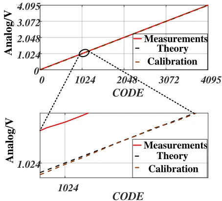
First, we use the first contrast calibration of lookup table method. The graph drawn by the calibrated values is shown in Fig. 2. Amplifying a certain section of the figure shows that although there is an error, compared with Fig. 1, the error is relatively small. The error of the measured value of this method can be controlled within 0.001V, which can meet higher application requirements under certain conditions.
0 1024 2048 3072 4095
CODE
0 1.024 2.048 3.072 4.095
1024
CODE
1.024
An
a
lo
g
/V
An
a
lo
g
/V
Measurements Theory
Calibration Measurements
[image:5.612.187.414.181.387.2]Theory Calibration
Figure 2. Error comparison after contrast calibration of lookup table method.
1024
CODE 1.024
1024 2048 3072 4096
CODE 1.024
2.048 3.072 4.095
An
a
lo
g
/V
Ana
lo
g
/V
Measurements Theory
Calibration Measurements
[image:6.612.192.398.57.264.2]Theory Calibration
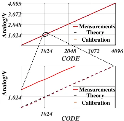
Figure 3. Error comparison after calibration of two-point method.
Finally, the calibration of adaptive method is used for the comparison test. The calibration points use the same points of the calibration of two-point method, and the automatic calibration time is set for 30 minutes. The error comparison curve drawn by the measured data is shown in Fig. 4. It can be seen from the comparison that the error can also be controlled within 0.002V.
1024
CODE 1.024
1024 2048 3072 4096
CODE 1.024
2.048 3.072 4.095
An
a
lo
g
/V
Ana
lo
g
/V
Measurements Theory
Calibration Measurements
Theory Calibration
[image:6.612.191.400.432.637.2]5. CONCLUSIONS
In order to improve the conversion accuracy of DACs, this paper studies the contrast calibration of lookup table method, calibration of two-point method and calibration of adaptive method based on FPGA. The contrast calibration of lookup table method is simple in theoretical analysis and has high calibration accuracy, but the operation process is complicated and the adaptability is weak. This method can be used when the number of DAC bits is small. The calibration of two-point method effectively improves the conversion accuracy on the basis of reducing the measurement data, calculates the correspondence between the digital code and the output analog quantity through two fixed points, and eliminates the offset error and the gain error to minimize the error. The calibration of adaptive method can automatically calibrate within the set time, which can effectively eliminate the error caused by the environment and external interference and improve the conversion accuracy. This method is suitable for environments with large DAC bits and complex environmental conditions.
ACKNOWLEDGEMENTS
This research was financially supported by Local Science and Technology Development Project Guided by Central Government (Grant No.2018ZYYD007), CERNET Innovation Project(Grant No.NGII20180615), Major Research Project Pre-research Fundation of Hubei University of Automotive Technology(Grant No. 2014XY02), and Key Laboratory of Automotive Power Train and Electronics(Hubei University of Automotive Technology) (Grant No. DK1201406).
REFERENCES
1. B. Ghanavati, E. Abiri, A. Keyhani, M. R. Salehi, A. Sanyal. 2018, “An energy efficient SAR ADC with lowest total switching energy consumption.” Analog Integrated Circuits and Signal Processing, 2018, 97(1): 123-133.
2. Deng Honghui, Zhou Fuxiang, Fu Nianhua, Fu Zhenda. 2018, “An 8 bit High Linearity DAC for Foreground Calibration.” Microelectronics, 2018, 48(02): 156-161+166.
3. Zhang Junke, Pan Wenyu, Yu Liuling. 1993, “Offset and Gain Adgustments of Analog Devices DAC and ADC.” Computer Engineering & Science, 1993(01): 92-96.
4. Singh, P. R., Pandey, B., Kumar, T., Das, T., Pandey, O. J.2014. “Output load capacitance based low power implementation of UART on FPGA.” International Conference on Computer Communication & Informatics IEEE, 2014.
5. Esmaeil Fatemi-Behbahani, Ebrahim Farshidi, Karim Ansari-Asl. 2016, “A new approach to analysis of residue probability density function in pipelined ADCs.” Integration the VLSI Journal, 2016, 52: 51-61.
6. Yu Wang, Haigang Yang, Xin Cheng, Fei Liu, Tao Yin. 2012, “A fast foreground digital calibration technique for pipelined ADC.” Journal of Electronics (China), 2012, 29(5): 445-450.
7. J.W.Bruce, Peter Stubberud. 2000, “An analysis of harmonic distortion and integral nonlinearity in digital to analog converters.” Proceedings of the 2000 IEEE Conference on Circuits and Systems. 2000: 470-473.