2018 International Conference on Computational, Modeling, Simulation and Mathematical Statistics (CMSMS 2018) ISBN: 978-1-60595-562-9
Study on Improving the Absorption Efficiency of Uncooled
Infrared Sensor by Using Grating
Yu-feng ZHANG, Yang WANG, Yuan-qing WU, Chun-mei LIU,
Xiao-dong LU and Tao ZHOU
College of New Energy, Bohai University, Jinzhou, 121013, China
Keywords: Uncooled, Infrared, Detector, Plasmon resonation, Grating, Structure optimization.
Abstract. When heated by incoming IR radiation, an uncooled infrared sensor changes the
temperature variation into a voltage or a current signal, which is detected by the readout circuit. Uncooled infrared sensors are usually made by building cantilevers on CMOS circuits. However, their performance is limited by the low absorption efficiency. To improve the absorption efficiency of an uncooled infrared sensor, the surface-plasmon-resonance structure is proposed in this paper. By COMSOL, the variation of the infrared absorption efficient with the structure parameters is simulated and analyzed. An absorption efficient of 98% within a specified spectral band and 30.5% averaged within the whole wavelength range is reached by parameter optimization.
Introduction
The study of uncooled thermal imaging detector arrays was proposed in the 1960s and entered a period of rapid development in the late 1970s. In the past few years, uncooled infrared focal plane technology has been rapidly developed and has been successfully applied in military, commercial and civil fields. The use of uncooled thermal imaging detection arrays eliminates the need for a complex cooling system for the entire infrared thermal imaging system, and the cost is greatly reduced. The cooling sensors were replaced by uncooled infrared sensors which have light weight, low power consumption, small size, reliable performance and easy operation in many fields.
The most common method of a microbolometeris to use micromachining to make a suspension bridge on a CMOS readout circuit to realize. This article studies one of the resistive bolometers based on VOx materials, by using the film resistivity change with temperature, and then the photothermal signal received by the detector was changed into voltage signal detected by the detection circuit. In order to improve the absorption efficiency of this sensor for thermal radiation, a grating structure based on surface plasmon excitation was studied in this paper.
Surface plasmon polaritons are electromagnetic waves propagating on the surface of a conductor. Free electrons in metal will oscillate under the irradiation of the same frequency photons, SPPs was formed and propagated along the flat metal/dielectric interface when the light hits the metal surface. This excited state is confined near the interface and is distributed exponentially in the vertical direction.
The excitation modes of SPPs mainly include: prism coupler, excitated by total internal reflection; waveguide mode coupling excited by evanescent waves on both sides of the waveguide; strongly focused beam, satisfying the wave vector matching condition with a large incident angle provided by a high numerical aperture; coupled with a grating to generate grating vectors satisfying the wave vector matching conditions by light diffraction; near-field excitation, light waves containing no less than the SPPs wave vector are generated by the probe tip. In this study, the commonly used grating coupling method of solar cells is used to excite the plasmon, and the resonance wavelength is adjusted by the modulation of the grating period to improve the light absorption rate.
Device Model and Principle
The uncooled infrared detector designed in this paper is an infrared microbolometer based on a grating structure. The schematic structure is shown in Fig.1. A pixel diagram of an infrared detector with support cantilever arms for the entire pixel structure on both sides is shown in Fig. 1a, and a sectional view is shown in Fig.1b, who have five layers: grating, passivation layer, absorption layer, support layer, and reflective layer.
Grating is located in the upper part of the detector pixel and is deposited on the silicon nitride passivation layer. Silicon nitride materials are coated on the upper and lower sides of vanadium oxide to provide insulation on the one hand and support layers on the other hand to reduce heat loss, and form a suspended structure supported on substrate. The thermal insulation performance of the detector is a key factor affecting the detection rate, and the metal wires on both sides of the cantilever beam are in direct contact with the two ends of the vanadium oxide, and the bottom processing circuit is also connected to form a conductive loop. The bridge arm also takes into account three functions of mechanical support, thermal conduction channel and electrical channel.
The light is incident from the top, passes through the grating and is absorbed by the multilayer film structure. The temperature of the detector changes accordingly, which in turn causes a change in the resistance of the vanadium oxide. The peripheral circuit processing completes the light absorption detection. The main principle of the device design: the use of metal gratings for coupling, in order to form a surface plasmon wave that propagates laterally along the material surface at the interface between the metal and the dielectric material, then enhanced the absorption rate.
(a) Pixel
[image:2.612.215.396.345.594.2](b) Profile of new structure
Figure 1. Structure of pixel and profile of new structure.
Simulation
Surface plasmon resonance usually occurs at the interface between metal and dielectric, but metal oxides also have this effect, which can be expressed as follows:
2 2 2 2
11 / /
N
n m
m
c m m m
s
i i
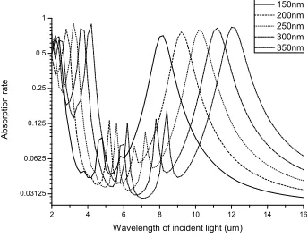
Ɛ∞is the high frequency dielectric constant, ɷn is the plasmon resonance frequency, ɷc is the attenuation rate, Sm is the oscillation intensity, ɷm is the resonant frequency, Гm is the linewidth, and m is the order of the Lorentz term.
COMSOL is used to simulate the light absorption characteristics of a grating detector structure. By comparing the influence of different structural parameters on the absorption efficiency of the detector, a more qualified model is optimized. In order to improve the computational efficiency, only one cycle of the device structure is analyzed. Using periodic boundary conditions on both sides, the material used for the metal grating is gold. The optical parameters are from the literature [9]. The optical parameters of VO2 are given in [10]:
Where Ɛ∞=3.95eV, ɷn=3.33eV, ɷc=0.66eV, and the Lorentz parameter is used as shown in table 1.
[image:3.612.229.383.267.353.2]The initial structure parameters of the detector were set as: grating period 5 μm, metal grating duty ratio 0.5, grating thickness 100 nm, Si3N4 passivation layer thickness 200 nm, VO2 layer thickness 100 nm, Si3N4 support layer thickness it is 300 nm and the bottom reflector is 300 nm.
Table 1. Parameter of Lorentz.
Sm(eV) ɷ(eV) Гm(eV)
1.816 0.86 0.95
0.972 2.8 0.23
1.04 3.48 0.28
1.05 4.6 0.34
Results and Discussion
Since the S-polarized light cannot generate the SPP wave, the default incident light's electric field direction is the x-direction. At this time, the incident light's polarization direction is parallel to the incident plane and is P-polarized. The incident light band is set to 2 ~ 20μm. The effect of the thickness of each layer on the heat absorption efficiency is simulated when the grating structure is not included. At the same time, when the grating structure is included, the influence of the parameters such as the duty cycle, period, and depth of the metal grating on the optical properties of the device in the mid-infrared waveband is considered, and the absorption spectrum is obtained.
Model Parameters Influence without Grating
The thermal sensor mainly reflects the device's ability to absorb and react to heat. From the point of view of the sensor structure, the silicon readout circuit is usually supported on the top of the silicon readout circuit by a thermally insulated microbridge made of silicon nitride with a small thermal conductivity, and the vanadium oxide film is deposited on the bridge surface. Heat-sensitive films, which are connected to the signal processing circuitry in the Si substrate via the leads on the two support arms. Most of the heat absorbed by the sensitive film can only be transferred from the support arm to the Si substrate, which reduces the thermal conductivity of the detector and increases the temperature variation caused by infrared radiation. Si3N4 is used as an infrared absorption film above the resistor. When infrared light is irradiated on the detector, part of the absorber is absorbed by the absorption layer, and the other part passes through the absorption layer and the sensitive film is reflected by the metal reflection layer and is again absorbed by the absorption film.
2.0 2.5 3.0 3.5 0.25
0.5 1
11 12 13 14 0.125
0.25
2 4 6 8 10 12 14 16 0.03125 0.0625 0.125 0.25 0.5 1 A bs orpti on rate
Wavelength of incident light (um)
[image:4.612.210.404.70.231.2]50nm 100nm 150nm 200nm 250nm
Figure 2. Influence on absorption efficiency of the passivation layer without grating.
It can be seen that the thickness of the passivation layer directly affects the first absorption peak with an incident wavelength between 2-3 μm. As the thickness of the passivation layer increases, the absorption rate of the first absorption peak decreases significantly. At the same time, accompanying the second absorption peak at a wavelength of 10-14μm produces a red shift.
At the same time, the thickness of vanadium oxide will also greatly affect the absorption efficiency of the device (Fig. 3). From the calculation results of vanadium oxide thickness, it can be clearly seen in Fig. 3 that the thickness of vanadium oxide influences the absorption efficiency and the absorption spectrum. The line undergoes a significant red shift as the thickness of the vanadium oxide changes, so that the position of the second absorption peak can be modulated by the thickness of the vanadium oxide.
2 4 6 8 10 12 14 16 0.01563 0.03125 0.0625 0.125 0.25 0.5 1 Absorpt ion rate
Wavelength of incident light (um)
100nm 150nm 200nm 250nm 300nm
Figure 3. Influence on absorption efficiency of VOx without grating.
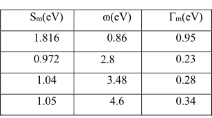
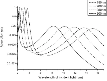
Model Parameters Influence with Grating
After adding a grating structure to the device, the absorption spectrum of the device is changed. The results are shown in Fig.4 and Fig.5 respectively. From the calculation results, they reflect that the enhanced grating structure causes significant changes in the absorption spectrum of the device, and the absorption peaks from 2 this changed to four. A new absorption peak appeared at a wavelength of 4 μm, a small absorption peak appeared at 8 μm, and the original absorption peak between 10-12 μm changed significantly, and the absorption efficiency at a specific wavelength can exceed 95%.
[image:4.612.211.386.396.529.2]2 4 6 8 10 12 14 16 0.03125 0.0625 0.125 0.25 0.5 1 A bs or pti on r at e
Wavelength of incident light(um)
[image:5.612.213.384.70.203.2]100nm 125nm 150nm 200nm 250nm
Figure 4. Influence on absorption efficiency of the passivation layer with grating.
2 4 6 8 10 12 14 16 0.03125 0.0625 0.125 0.25 0.5 1 A b so rp tio n r a te
Wavelength of incident light (um)
150nm 200nm 250nm 300nm 350nm
Figure 5. Influence on absorption efficiency of VOx with grating.
It is due to plasma absorption between the grating structure and the passivation layer, ie, SPP wave, the electric field is located inside the passivation layer, so that the propagation and absorption of the SPP wave are closely related to the thickness of the passivation layer, and the thickness is greater and the absorption is higher.
The absorption efficiency of vanadium oxide did not change significantly, and the thickness was still the peak position of the absorption line. As the thickness increases, a red shift of the spectral lines occurs.
[image:5.612.211.383.239.372.2]Figure 6. Influence of rectangle size on absorption efficiency of rectangular double period grating.
Figure 7. Effect of rectangle size on absorption efficiency of circular double periodic grating.
Figure 8. Influence of grating thickness on absorption efficiency.
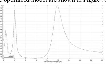
Optimized Model
The optimized parameters are: mother grating period 3 μm, sub-grating period 0.03 μm grating thickness 1 nm, Si3N4 support layer thickness 200 nm, VO2 layer thickness 350 nm, and Si3N4 passivation layer thickness 200 nm.
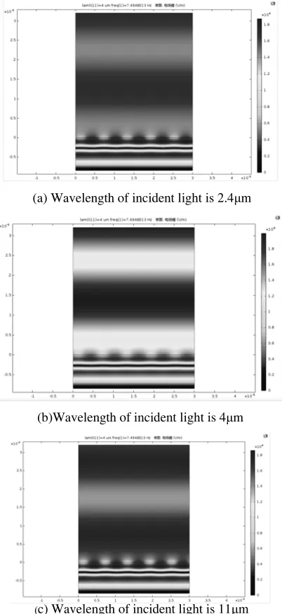
[image:6.612.230.376.395.508.2] [image:6.612.216.402.607.719.2]There are 3 main absorption peaks in this structure, the highest absorption efficiency wavelength is between 10-14μm, which is 99.65%, absorption efficiency of 4μm wavelength up to 92%, the device can get a good optical absorption effect. The average absorption efficiency reached 31.4% over the entire wavelength range. The distribution of the electric field is shown in Fig. 10 corresponding to the three absorption peaks.
(a) Wavelength of incident light is 2.4μm
(b)Wavelength of incident light is 4μm
[image:7.612.206.407.138.575.2](c) Wavelength of incident light is 11μm
Figure 10. The electric field distribution of the three absorption peaks.
Conclusion
Acknowledgment
This paper is supported by National Natural Science Foundation of China (NSFC), No. 61575029; The preferred spelling of the word “acknowledgment” in America is without an “e” after the “g”. Avoid the stilted expression, “One of us (R. B. G.) thanks” Instead, try “R. B. G. thanks”. Put sponsor acknowledgments in the unnumbered footnote on the first page.
References
[1] Young Chul Jun, Edward Gonzales, John L Reno, et al. Shaner, Alon Gabbay, and Igal Brener, Active tuning of midinfrared metamaterials by electrical control of carrier densities [J]. Optics Express, 2012, 20(2): 1903 1911.
[2] Guo Nan, Hu Wei Da, Chen Xiao Shuang, et al. Enhanced plasmonic resonant excitation in a grating gated field effect transistor with supplemental gates [J]. Optics Express, 2013, 21: 1606 1614.
[3] Yu Miao, Gao Jin-Song. Suppression of the stray light of 2-dimensionalgratings combined with an array of periodic slit [J], Acta Phys. Sin. Vol. 62, No. 20 (2013) 204208.
[4] Zhou Jun, Sun Yongtang, Design of a highly efficient light-traping structure for amorphous silicon solar cell [J], Acta Phys. Sin. Vol. 60, No. 8 (2011) 088802.
[5] Jiang Wenjing, Ou Wen, et al, Improved structure for SOI diode uncooled infrared focal plane arrays [J], J. Infrared Millim. Waves, Vol. 33, No.1 February, 2014, 218-221.
[6] A. Hessel, A.A. Oliner. A new theory of Wood’s anomalies on optical gratings. Appl. Opt. 1965, 4(10): 1275-1297.
[7] Wang Lin, Hu Wei Da, Wang Jun, et al. Plasmon resonant excitation in grating gated AlN barrier transistors at terahertz frequency [J]. Applied Physics Letters, 2012, 100: 123501.
[8] Zhong Min, Influence of hole shape on the transmission and negative refractive index properties of metal-dielectric-metal metamaterial [J], J. Infrared Millim. Waves, Vol. 33, No. 3 June, 2014, 227-230.
[9] Ordal M.A., Long L.L., Bell R.J., et al. Optical properties of the metals Al, Co, Cu, Au, Fe, Pb, Ni, Pd, Pt, Ag, Ti and W in the infrared and far infrared [J]. Applied Optics, 1985, 24(24): 4493 4497.