6
II
February 2018
Electrical Characterization of SnO
2
based thick
film resistors loaded with an optimized Sb: Sn
alloy
B. R. Sharma1, S U Shinde2, N. D. Chaudhari3
1,2,3
Dept. of Physics Pratishthan Mahavidyalaya Paithan, Dist Aurangabad, M.S.
Abstract: Thick Film Resistors (TFRs) are extensively being used in hybrid electronic technology, wherein high standards of electrical parameters and stability in changing thermal environment are required especially in space-research based industries. In the present paper, the optimized alloy Sb0.6:Sn0.4 of 5-10μm size was loaded in SnO2nano-sized powder
synthesized by sol-gel method, to produce range of resistive pastes. Thick Film Resistors fabrication and their electrical and material characterization using XRD and SEM studies have been reported. The fall in sheet resistivity ρs against loading
fraction of optimized alloy Sb0.6:Sn0.4 in SnO2nano-sized particles has been examined using percolation/effective medium
theory.
Keywords: Thick film resistor, Sheet Resistivity, TCR, Firing Temperature.
I. INTRODUCTION
The hybrid microelectronic thick film technology has been extensively used wherein the screen printed films are fired at high temperature can be used as planar passive components, such as, resistors, capacitors, conducting terminations etc. However thick film pastes/inks are based on expensive noble metals like Ru, RuO2, Pd, gold, etc. The Thick Film Resistors (TFRs) are superior in
performance, such as stability against load, low thermal noise, high current carrying capacity, non-inductive in nature, could be used at high frequencies1-3.The cost effective SnO2nanoparticles can be easily synthesized by sol-gel method, may be used as a functional
material in the composition of TFR pastes4-6. S.H. Bhide et al used antimony as a dopent (5% by weight) in SnO2 and reported sheet
resistivity of 1MΩ/□and temperature coefficient of resistance (TCR) about -2000 PPM/ ⁰C 7. M. R. Kadam et al reported that the film resistive pastes using SnO2 as a functional material and loaded by SnCl2gives the minimum sheet resistance as ρs= 5 KΩ/□and
TCR (α) as low as -950 ppm/°c and the paste containing SnO2 : (Sb 5%) loaded by SnCl2 resulted in the range of various resistive
pastes8. Further Kattimani et al reported when Sb:Sn alloy loaded in SnO2results in sudden fall in sheet resistivity at 5 % of Sb:Sn
doping from 1012Ω/□ to 750 Ω/□ followed by continuous steady decrease of resistivity and TCR at 90 % Sb:Sn alloy loading at 170 Ω/□ and TCR about -950 ppm/°c9. The research in nanoparticle physics is of interest due to high sensitivity for hydrogen, humidity, and LPG gas sensors4-6,10.It is interesting to study electrical properties in the variation of optimized Sb0.6:Sn0.4alloy of 5μm size
loaded in SnO2nano-sized particles as cost effective thick film resistors. The fall in resistivity over the whole range of weight
fraction Wmin SnO2 based thick films is predicted/expected to be similar to B. E. Springette’s percolation model based on
conducting particles mixed in uniform dielectric matrix11.
II. EXPERIMENTAL PROCEDURE
A. Synthesis of SnO2 and Sb:Sn Alloy
The Stannous Oxide (SnO2) nano-sized particles were synthesized using standard sol-gel technique. The SnC14.5H20 (AR grade)
was dissolved in distilled water to make a 0.1 M solution. The prepared solution of SnC14 and H20 was mixed with ammonia
(NH4OH, AR grade). The resulting precipitation was washed thoroughly with distilled water for longer times to remove excess (C1
-and NH4+) Ions. The filtered resulting milky-white cake / gel were dried for 24 hrs at 100 °C under the IR lamp. The dried
precipitate was ground into fine powder using agate mortar pestle and filtered through a 250 meshsize nylon cloth. The resulting powder was sintered/ calcined for 4hrs at various temperatures (500-1100 °C) to obtainSnO2fine particles of various sizes ranging
removed/collected by breaking quarts tubes and crushed in agate mortar pestle and ball milled for 12 hrs in acetone medium, dried under IR lamp then filtered through 250 mesh nylon cloth, ready to mix in SnO2 to formulate the paste and TFRs.
B. Preparation of SnO2 based Sb:Snalloy thick film Resistors
The Stannic oxide fine powder prepared by the above method was used as the basic functional material. The SnO2based on
optimized Sb0.6:Sn0.4 alloy paste was prepared with 10 % of standard lead borosilicate glass frit as a permanent or inorganic binder;
ethyl cellulose (EC) and butyl carbitol acetate (BCA), were added suitably (solid to liquid ratio 70:30 by weight) so as temporary binder to get a thixotropic and rheological paste12. The paste was then screen printed on pure alumina (Al2O3) substrate (1״× ½״),
dried for 4 hrs then firedat 800°C using induction heating for 45 minutes. For good electrical contact Silver electrodes were printed and dried under IR lamp after firing the films. The film thickness, as measured by light section microscope (BK 70 × 50Carl Zeiss, Jena) with an accuracy of ±0.5 μm, varies from 20 to 30μm and it is normalized to 1 mil or 25μm. The d.c. resistance of the pattern with different aspect ratios (N = L/W = 1, 1.5, 2) was measured by digital electrometer (Keithley EA-614). The time-temperature profile of the induction furnace was chosen so as to give good adhesion of uniform thick film formulation without any blisters or holes. The thickness of the thick films were monitored by light section microscope and ρs is normalized to 25 μm thickness used to
measure sheet resistivity defined by
= = = ∙
(1)
in the units of Ω/□. Where, ρB, R, t and N are the values of bulk resistivity, resistance, thickness and the aspect ratio (N = L/W =
[image:3.612.82.462.358.439.2]length/width) for the thick film resistor test pattern respectively. Resistor test pattern is having length L and width W for different values of N.
Fig. 1.Schematic representation of resistor test pattern on alumina substrate. The temperature coefficient of resistance (TCR) is given by,
= ( )
( )
= ( )
( ∙ ∙ )∙10 / ° (2)
Where, R1 and R2 are the values of resistors at the absolute temperatures T1 and T2 in linear region over R-T Characteristics in the
range 30-130°C. The temperatures are monitored by temperature controller, based on alumel-chromel thermocouple using small resistive furnace.
C. X-ray analysis and Particle Size
The material characterization of TFRs was performed using X-ray diffraction and SEM techniques. Tin oxide occurs in various phases: orthorhombic, tetragonal, cubic or triclinic. But here only the tetragonal phase was revealed in x-ray analysis13.X-ray diffraction analysis of tin oxide powder calcined at various temperatures500-1100 °C, as well as alloy powders made into thick films (suitable for resistors) was carried out using Philips PW-1840 diffractometer. Standard CuKα radiation line having wavelength
λ = 0.1542 nm was used as the X-ray source. The higher peak intensities of XRD pattern analysis reveals polycrystalline nature due to bigger grain size in the agglomerates of all the thick film resistors. Particle size analysis was made using the FWHM (β) width of the prominent diffraction peak and using the Debye-Scherrer formula,
Dhkl= 0.9λ/β cosθ (3)
Where Dhkl is the diameter of the particles in the hkl direction,λ is the X-ray wavelength of source and β is the full angular width of
the diffraction peak at half the maximum intensity for diffraction angle 2θ in radians. From the Fig. 2, it is observed that the particle size D in the range 28-52 nm increases linearly with the curing temperature T, indicating growth of crystallite grains.
Silver Electrode
Resistor Test
III. THEORETICAL CONSIDERATIONS
B. E. Springette proposed effective medium theory that assumes insulator to be continuous medium in which spherical metal particles are randomly embedded. The simple cubic lattice model can be used for particulate system to explain the effective conductivity of the medium. As more and more metal particles are introduced, the lattice sites become more occupied in a random manner with each lattice site is associated a conductivity σi whose value depends upon whether the site is occupied by by metal or
insulator. In this way network of electrical conductance is developed. The probability Pi that a site is occupied by metal particle is
Vm/f where Vm is the volume fraction of the metal and f is the packing fraction. For simple cubic, BCC and FCC f takes values
0.528, 0.68 and 0.74 respectively11,13-14.Assume that all conductances are equal to . Let one conductance be changed to back to its true value σi , examine the voltage difference between the Viand the voltage across σiand voltage across far from σi is V. the
conductance of the adjacent nodes of the network of conductances = (1/2)z where z is the coordination number of the lattice. Consider such pair of nodes and consider the conductance across it, replacing the rest of the network by a conductance σn. If the
current flowing in to the lattice is I, then all the conductances are equal to , the voltage drop across the node is given by11,
=
( + )= ̅
There fore = [ −1] where is replaced by σi the voltage drop becomes,
=
( + )
= ( + )
( + )
Substituting for , − ̅ = ̅( − ) [⁄ + ( −1) ]
By the definition of , as all the conductances are replaced by their original values, ( − ̅) should be averaged to zero. Thus if P(σ) is the probability distribution of the conductance σ, we have for the cubic network,
∫ ( )( )
( ) = 0 (4)
where P(σ) is a binary distribution, σm is the metallic conductivity, σα is the insulator conductivity, then the above equation
becomes,
( )
( ) +
( )
( ) = 0 (5)
This is a quadratic equation for where the root is given by,
4 = [ ′ + ′ ] + [( ′ + ′ ) + 8 ] /
or the average conductivity
= [ ′ + ′ ]/4 +
′ ′
(6)
Where,
′ = (2− ) (7)
′ = ( −1) (8)
If and are known experimentally then ⁄ ≈10 we can plot a graph of log ( ⁄ ) versus weight fraction or volume fraction of the metal in dielectric medium. For our experimental system SnO2nano-particles of average size nearly 50 nm are used as
continuous dielectric matrix along with glass frits of 10 μm size (10% by weight) mixed with optimized Sb0.6:Sn0.4 alloy particles of
5~10 μm size and varied as weight fraction wm in the fired pastes at 800°c. For [SnO2nano-particles +10% glass frits] the average
conductivity = 1.4 ∙10 Ω and the conductivity of the pure Sb0.6:Sn0.4 alloy = 0.122 Ω for [90%
IV. RESULTS AND DISCUSSIONS
As the XRD analysis show that Sno2 and Sb0.6:Sn0.4alloy decomposes in to free metal and metal oxides during the firing process.
The experimental values for and 1.4x10⁻¹⁰Ω-1 cm-1and 0.122 Ω-1 cm-1 are used for the calculation of Log of conductivity ratio (σα/σ̅ )respectively, by using equations(6,7,8). The Springette’s theoretical and experimental curves in percolation threshold
differ on account of decomposition of SnO2 and Sb:Sn alloy in to free metals Sb , Sn and their oxides during firing process as
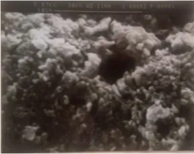
revealed by XRD analysis, wherein their relative conductivities may not remain constant (Fig.3), as model considers it for constant conductivities of and for full range of weight fraction Wm in SnO2. Also the fired films are not homogeneous and uniform in
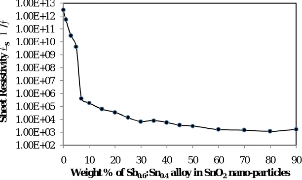
microstructure and may develop pin holes and agglomerates as revealed by SEM micrographs Fig.6(a) to 6(d). The sheet resistivity and temperature coefficient of resistance (TCR) shows similar falling trend with loading percentage of Sb0.6:Sn0.4alloy in SnO2
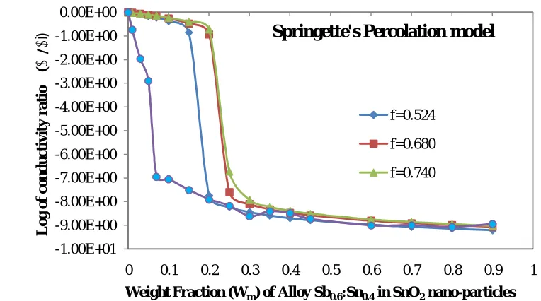
nano-particles.Theoretical and experimental comparison of log of conductivity ratio and weight fraction is shown in Fig. 3, where it is observed that theoretical percolation threshold or sudden fall in conductivity ratio is observed with the weight fraction wm ~ 0.3,
however experimentally the percolation is observed at wm ~ 0.07. This discrepancy in the values of model prediction of percolation
[image:5.612.177.438.294.453.2]and observed percolation may be explained on the basis of non-spherical nature of particles and porosity of the fired polycrystalline nature of thick films as seen in the SEM micrographs. The chemical reactions occur during firing process may alter electrical conductivity of the alloy and free metal particles as revealed by XRD analysis.
Fig.2. Variation of particle size of SnO2 with Curing Temperature
Fig. 3.The variation of electrical conductivity ratio Log (σα/σ̅) versus Wt.
28.51 35.81 37.94 45.5 52.94 20 25 30 35 40 45 50 55
400 600 800 1000 1200
P ar ti c le S iz e D i n n m
Curing Temperature T ⁰C Stannous-Oxide particle size D in nm
-1.00E+01 -9.00E+00 -8.00E+00 -7.00E+00 -6.00E+00 -5.00E+00 -4.00E+00 -3.00E+00 -2.00E+00 -1.00E+00 0.00E+00
0 0.1 0.2 0.3 0.4 0.5 0.6 0.7 0.8 0.9 1
Lo g o f c o n d u c ti v ity r ati o ( σα / σ ̅ )
Weight Fraction (Wm) of Alloy Sb0.6:Sn0.4in SnO2nano-particles
Springette's Percolation model
f=0.524
f=0.680
[image:5.612.107.489.500.713.2]fraction of Sb0.6:Sn0.4 alloy in SnO2nano-particles along with
[image:6.612.156.462.116.299.2]Springette’s percolation model.
[image:6.612.147.470.337.521.2]Fig. 4. The variation of electrical sheet resistivity (ρs) versus weight % of Sb0.6:Sn0.4 alloy in SnO2nano-particles.
Fig. 5. The variation of Temperature coefficient of resistance (α) versus weight % of Sb0.6:Sn0.4 alloy in SnO2nano-particles.
Fig. 6(a):90% Sb0.6:Sn0.4 alloy + 10% glass frits Fig. 6(b): Pure Alumina substrate (Etched) 1.00E+02 1.00E+03 1.00E+04 1.00E+05 1.00E+06 1.00E+07 1.00E+08 1.00E+09 1.00E+10 1.00E+11 1.00E+12 1.00E+13
0 10 20 30 40 50 60 70 80 90
S h e e t R e si sti v ity ρs Ω / □
Weight % of Sb0.6:Sn0.4alloy in SnO2nano-particles
-12000 -10000 -8000 -6000 -4000 -2000 0
0 10 20 30 40 50 60 70 80 90
TC R α p p m /° C
[image:6.612.125.515.562.707.2]Fig. 6(c): 45%SnO2 + 45%Sb0.6:Sn0.4 alloy + 10% glass Fig. 6(d): 87% SnO2 + 3% Sb0.6:Sn0.4 alloy + 10%
Fig. 7(a): XRD patterns of Sb:Sn alloys prepared Fig. 7(b): XRD patterns of SnO2 based Sb0.6:Sn0.4with different compositions
heated at 630 oC . alloy loaded TFRs fired at 800 oC
V. CONCLUSIONS
The electrical characterization of SnO2nano-particle based thick film resistors loaded with an optimized Sb0.6:Sn0.4 alloy that gives
minimum sheet resistivity and TCR was used to produce in the range of sheet resistivity of thick film resistors from 3x10¹²Ω/□ to 1.71 k Ω/□ and TCR in the range -3145 to -814 ppm/ oC. Further theoretical and experimental values of percolation threshold observed at 0.2-0.3 and 0.07 weight fractions, differ on account of ideal assumptions for the Springette’s effective conductivity model, wherein spherical alloy particles with constant conductivity metallic particles were supposed to be embedded in SnO2
insulating matrix. The model needs modification for non-uniformity of microstructure and carefully designed experiments.
REFERENCES
[1] Dr K S Murthy, Short term courses on thick and thin films hybrid circuits, Sept. 1986, IISc., Bangalore,
[2] Toshio Inokuma, Y. Taketa and M Haradome, Conductive and insulative particle size effects on the electrical properties of RuO2 thick film resisters, IEEE,
1986, Vol. CHMT-8, No. 3.
[3] Dr. K Ramkumar, Thick film deposition and processing, Short term course on thick and thin hybrid microelectronics, 1986, Bangalore.
[4] S G Ansari et al Effect of thickness on Hydrogen gas sensitivity of snO2 nanoparticles based thick film resistors, Journal of materials science Materials in
Electronics, 1996, Vol. 7, pp267-270
[5] S. G. Ansari et al The effect of humidity on an SnO2 Thick film planar resistor, Sensors and actuators, 1994, Vol. 21(3), pp. 159-163.
[6] R Y Borse and A. S. Garde, Electrical and gas sensing properties of SnO2 thick film resistors prepared by Screen-printing method, Sensors and Transducers,
[image:7.612.323.513.98.249.2] [image:7.612.96.527.280.469.2][7] S H Bhide et al, Formulation and characterization of tin oxide based resistive pastes with Sb doping, International Journal of Hybrid Microelectronics, 1988, Vol. 11, pp. 36-39.
[8] M R Kadam et al Electrical Characteristics of SnO2 –based thick film resistors loaded with Sncl2, Thin Solid films, 1990, Vol. 187, Issue 2, pp. 199-208.
[9] V K Kattimani, R N Karekar R C Aiyer, Electrical properties of SnO2:Sb based thick film resistors loaded with SbSn alloy, Int. J. Hybrid microelectronics,
1991,Vol.14.
[10] TriptiShukla, Synthesis of tin Oxide thick film and its investigation as a LPG sensor at room temperature, JST July, 2012, pp., 102-108.\
[11] B E Springette, Coductivity of a system of metallic particles dispersed in an insulated medium, Journal of Applied Physics, 1973, Vol. 44, No. 6.
[12] E R Cubellio et al., Effect of the addition of different metal oxides in lead borosilicate glasses on the electrical characteristics of SbSn composition-based
thick-film resistors, Active and Passive Ele. Comp. 1993, Vol 16, pp. 7-18.
[13] F. Bucche, Electrical resistivity of conducting particles in an insulating matrix, Journal of applied Physics, 1972, Vol. 43, No. 11, pp.4837-38.