DISTRIBUTION IN LOW POWER CLOCK USING MULTIPLE
VOLTAGES AND REDUCED SWINGS
1
Peeyush Agarwal, 2Arvind S.M., 3Sangya Thakur, 4Paras Dhama,
1,2,3,4
SRM University Kattankulathur, India.
ABSTRACT
Significant fractions of the dissipation in power of a chip is accounted by clock networks and are critical
to performance. The algorithms and theory for building a low power clock tree is presented in this paper
when at a lower voltage, the clock signal is distributed and is translated to a voltage which is high at the
utilization points. The low power schemes to be used are two: reduction in swing and many supply
voltages. The issue of construction of tree and present conclusions which are relevant to many
technology generations as per the NTRS are analyzed.
INTRODUCTION
One of the most important parts of a synchronous VLSI chip are constituted by the clock signal as it can
influence the area, power dissipation and speed of the system.
Power dissipation is one major drawback associated with clock networks. It is shown in studies that the
power dissipated by clock network is 20-50% of the total power on a chip. Strategies for significantly
reduction in the power dissipation of the clock network are needed to develop ,the work in this paper is
based on the observation that the clock network can be made to dissipate less power by using a lower
Vdd to distribute the signal over the chip.
Research has been done on the problem of clock tree synthesis for zero skew. A recursive bottom-up
combination of two zero-skew subtreeshas been performed by this method by finding a tapping point
which ensures zero skew in thesubtreewhich is larger. A method called The Deferred-Merged
Embedding (DME) embeds a given clock tree topology optimally in the Manhattan plane with skew of
Controlling ofthe short circuit dissipation of power isdone by the enforcement of a constraint that the
clock edge should never have a transition (rise/fall) time larger than a given specified time throughout
the clock tree.
The below stated equation lists the expression for the charge/discharge power dissipation.
P = ƒCLVddVsequation 1
Whereclock frequency is f, load capacitanceis the CL, supply voltage is the Vdd, and the output swing of
the buffer is Vs. In the cases where the output of the buffer swings from 0 to Vdd, Vs andVddhave the
same value and the formula reduces to P = f CL Vdd2.
Since fundamental parameter for the circuitisf, no changes can be made and the reduction in its effects
can only be done by techniques like clock gating.
Therefore, the reduction in the dissipation of power in the clock network can only be made by
(a) Reduction in the total load capacitance, thatis consistent with attempting which leads in achievement
in the minimal wire length and the minimal power dissipation in buffer.
(b) Reduction in Vdd, which leads to a quadratic reduction provided there is also simultaneous reduction
in Vs by the same factor.
(c) Reduction inVs without a reduction inVdd, which is corresponding with a linear reduction in the
dissipation of power.
A new theory is presented in this work and results for building low power clock trees using a smaller
voltage to distribute the signal over the chip, and then converting this low voltage clock signal is done
back to a higher voltage at the utilization points.
1.STATEMENT OF THE PROBLEM
1.1Structure of the Clock Tree
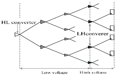
Figure 1: Low Power Clock Scheme
In order for the regeneration of the signal and maintenance of a sharp slew rate when the signal goes
through the network, the use of immediate buffers is recommended in the clock tree. It is proposed in
this paper, an HL converter is inserted without giving a justification that is specific, at the root of the
clock tree, , and at the clock sinks, LH converters are inserted,which finally leads to the placing of the
entire clock tree in the region of low voltage.
1.2Level Converter Circuits
1.2.1A Level Converter Using Multiple Supply Voltages
The need is to convert the clock swing from a voltage range which is high of gnd to VddH to a voltage
range which is low of gnd to VddL.For ensuring that there is no transient current which is having
significance,the part whichVddH drives is having more usage of feedback which helps to speeding up of
[image:3.612.54.246.87.212.2]the transition.
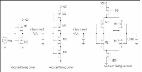
1.2.2A Level Converter by the use of Reduced Clock Swing
Output clock swing isanother variable that can be adjusted so that dissipation of power is reduced as
explained in equation (1). For the problem of clock tree, there would be delay and transition times by the
use of a driver to drive a long interconnecting wire without the use of any repeater drivers. A clock
scheme with reduced-swing is presented with drivers in this paper, as illustrated in Figure 3. The driver
having reduced swing is shown in Figure 3 and its output swings that change its valuefrom Vtn to Vdd
-|Vtp|.For acting as an inverter, M4 and M5 are there and M3 and M6 change the ground and supply
voltages to Vdd-|Vtp| and Vtn, respectively, hence ensuring a zero steady-state short circuit current and
[image:4.612.55.293.318.440.2]keeping both the output swing and the input swing same.
Figure 3: Clock Scheme withReduced Swing
Finally, there is a modification version of the fully complementary Self-Biased CMOS differential
amplifier, the reduced spring receiver. By feeding back the output signal to the other differential input
node, the modification is performed.
A few comments about the circuits above are in order:
1. The transistors will have to be sized appropriately.
2. The transistors M3 and M6which are present in the reduced swing buffer.When the output voltage
reaches Vdd-|Vtp| [Vtn] makesthe output swing limited by turning off a path to Vdd [ground].
Availability of discharge path is negligibleto reduce the voltage back to Vdd-|Vtp| if the voltage on the
connected wire rises above Vdd|Vtp| due to the reason of coupling with another wire.Unexpected
3. The outputs of the reduced swing buffer can rise towards Vdd or fall towards ground due to the
leakage currents, it is also dependent on the polarity the output stateis having, if the clock is stopped
for a period of time so that power can be saved. As a result, unexpected skews can be seen in the
first clock cycle after the reactivation of the clock is done. By the usage of a design discipline that
starts the clock one or more cycles earlier to when it is required to be started,this may be overcome.
4.The delays in the given circuitsare susceptible to effects of noiseand noisehaving power supplysame
as the onesdescribed in item 3.
INSERTION OF BUFFER
The possibility of buffer insertion at the base of the twosubtrees which are child is considered after
joining of each pair of sub trees. For a buffer to be inserted, the criterion is that the slew rate at each
buffer input and each sink node is faster than a specified given amount.
There are two reasonsthat the LHconvertersare placed having a major impact on the dissipation of power
of the clock tree:
(a) More numerous converters than any other type of buffer are LH convertersas the converters which
are at the lowest stage of the clock tree are LH converters.
(b) A larger amount of power per unit wire lengthis consumed by the wires downstream of the
LHconvertersbecause they are driven at the high swing.
An important role is played in the total power dissipation of the tree by the positioning of LH converters.
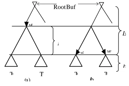
1.3Theoretical Results on Buffer Positioning
Thecriteria which isused to determine the results determine the positions of the LHconverters, by using a
common area measure that gives an estimation of it as the sum of buffer widths.
Theorem 1:For the buffer area solution to be minimum,the insertion of LH converters is necessary at
the clock sinks, appropriately sized so that the clock slew rate constraints can be met.
Proof: Lettwo subtreesT1 and T2 be taken that are zero-skew merged to form asubtree which is large, as
it is shown in Figure 4. Two options are considered for the possibility of inserting an LHconverter in this
(a) The subtreeformed by merging T1 and T2is driven by an LH converter if size w1
(b) LHconverters of size w2 and w3,drives T1 and T2respectively
The sizes of LHconverter are chosen that requirements of edge rate for each subtree are not be met by
the use of same size of LH converter.
Figure 4: Buffer Placement
[image:6.612.65.271.183.320.2]W1 must be greater than w2+w3in order for option (b) to be an area-optimal solution.
Figure 5: Buffer Sliding
Asubtreedriven by a buffer as shown in figure 5, of which characterization is done bythe delay
downstream, tdand the capacitance downstream, C,. The relationship between w and w′ can then be
given as:
t/2=k/w`(C+lC) + r0l C+ lC0/2+ t d = (k/w) c+t
Wheretdand Care, respectively, the downstream delay and capacitance of the location of buffer w, the
length of the segment along which w is moved up to w’ is l, and k, r0and C0are respectively, the unit
resistance of buffer, the unit resistance of wire and the unit capacitance of the wire. This leads to the
relation
1/w’ (1+lC/C) + r0l/k (1+lC/2C) = 1/w
Since it can be clearly seen that the factor of multiplication for 1/w’ ismuch larger than 1 and a positive
number is added to the quantity, this gives us a result 1/w> 1/w’, i.e., w’ >w.
C, t d
w w ′
l
L 1
L 2
w 3
w 2
w 1
l
( a) ( b
) T 2
T 1 T 1 T 2
Therefore, when Figure 4(b) which has both the buffers are made to slide up until they are just merging
point downstream, as shown in Figure 6(b) the size w2’>w2and w3’ >w3.
For the transition time requirement to be satisfied at the leaf nodes, the following relationship must hold.
K / w2′ ((l1 + l2 )Co+ C1 + C2 ) + rol1 Col1+ C1 + td1 =k (l1Co + C1) + rol1 Col1+ C1 + t w1 2
When we simplify the following expression, it is found that the relationship between w2’ and w1is 2.
w2′ = (l1C0’C1)/ ((l1+l2)Co+C1+C2)w1=(Cleft/Ctotal)w1
Where the sum of the capacitance downstream in both sub trees isCtotal andCleftis the total capacitance
downstream in the sub tree which is on left.Similarly, it can be definedthat Crightis the total capacitance
in thesubtree which is on the left, the expression for w′3 can be derived as
w3′ = (l2C0’C2)/ ((l1+l2) Co+C1+C2)= (Cright/Ctotal)/w1
Therefore, adding (5) and (6), we obtain the result
w1 =w′2 +w′3(7)
The scenario that is shown inFigure 4 (a) is much worse than that in Figure 4(b) when buffer areais
considered asw2′ and w3′ are greater than w2 and w3 respectively, and alsow1 = w2’ + w3’.Positioning an
LHconverter in the tree at lower place is considered to result in cost of smaller area as long we know
that the size of LHconverter is always proportional.
Next, Two scenarios are considered in terms of the dissipationof powershown in Figures 4(a) and 4(b).
As beforetransition time constraints at the sinks are met with each of w1, w2and w1.
P=k1w+k2(8)
The output stage is assumed to be sized in such a way that the ratio of the NMOS transistor to the PMOS
are equal.
Therefore, as the scenario of Figure 4 is considered, in order for option (a) to be better than option (b),
the following condition must hold: k1 w1 + k2 + k3(L1- l) + k4 (L2+ l) < k1 w2 + k2 + k1 w3 + k2 + k3 L1 +
k4 L2 (9)
Where k3 = ƒVddL2Co and k4 = ƒVddH2Co.
Theorem 2: The power in the clock tree P1is considered at a specific positioning of the LHconverters,
which is sized to meet the transition time constraints at the sinks. Let the power corresponding to
LHconverters be P2which is inserted at any location which is high in the tree, appropriately sized to
satisfy transition time constraints. The dissipation of power P1< P2but the following condition should
hold: k2>k1(w1− (w2+w3)) +l (k4−k3) (10)
Proof: Immediately followed from a simplification of (9). It is stated in the inequality in (10) that k2
must be greater than the sum of the dissipation of power due to the increase in size of the buffers.
In order for (10) to be true, k2>k1(w1-(w2+w3)) and k2>l(k4-k3), as we can see that both terms of the right
hand side are positive The expression of the latter condition can be given as l < k2/(k4-k3)
Technolo
gy
250 180 150 130 100
VddH/VddL 1.38 1.2 1.25 1.25 1.33
Maximum
l
Table1: Required and Average Wire length
2. PROPOSED ALGORITHM
2.1 Outline of the Algorithm
The major difference is in the usage of an HLconverter at the root of the tree and at various points in the
clock tree, the use ofLHconverters.
Algorithm Bottom-up Buffer Insertion
INPUT: set of sinks S, technology parameters OUTPUT
Tree of buffered merging segments
BEGIN
A = S /* A being a set of non-buffered segments */
B = Φ /* B being a set of buffered segments */ while (|A| > 1 or |B|
> 0 ) if ( |B| > 0) and (|A| = 0)
A = B; B = Φ /*if A is empty and B is non-empty, swap them*/
G (E, V) = DT (A); /* Build Delaunay Triangulation on A */}
I = Find_independent_edges (G);
A = A - {b, c} if (buffer insertion criterion satisfied)
b= insert buffer (b);
c= insert buffer (c);
Benchmar
ks
r1 r2 r3 r2 r5
Avgl to
first
buffer
a= zero merge (b, c);
B=B U{a}
Else
A=A U{a}
END
Figure 7: Algorithm Hierarchical Clustering-Based Buffer Insertion
A Delaunay Triangulation on Ais built, and then a nearest neighbor graph is constructed. Form A, the
two merged segments will be deleted and the new merging segment will be checked to see whether the
transition time constraint is satisfied. Once the first level of clock buffers is added, the sets A and Bare
swapped, the whole procedure is repeated again. The algorithm is proceeded until only one node is left
and AandB is empty. At this point, a tree of segments is returned by the procedure.
Property: It is ensured by algorithm of Bottom-up Buffer Insertion that there will be an equal number of
buffersfor any path from the root to the sinks.
2.2 Finding a Minimum Power Solution
For each merging point, a tuple [Solbuffered,Solunbuffered] is stored. The parameters Sbuffered and Sunbuffered
give the best solution for the situation where an LH converter has been added or has not been added to
the downstream subtree. At the current level the two Sunbuffered solutions are combined to create
aSunbufferedsolution,whenever two sub trees are merged. ASbuffered solution may be created either by
combination of the two Sbuffered solutions from the subtrees, or by combination of the two Sunbuffered
solutions and an LHconverter is placed at the merging point, which is sized so that the transition time
requirements are met at the leaf nodes. This is continued up the tree until the maximum sizeis less than
the required buffer size, and this is the point where the optimal solution is chosen.
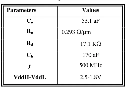
Thereare five benchmarks on which our algorithm was tested. The parameters that are used are based on
a 250 nm technology and are listed in Table 2. The unit driver resistance is R0; all other parameters are
as described earlier.
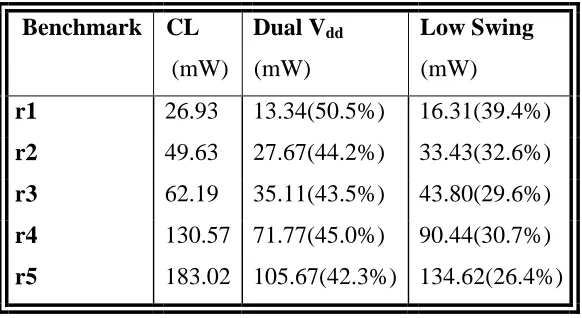
The comparison of power dissipation between algorithms CLisshown in Table 3 which is augmented
with a buffer insertion algorithm and our algorithm. The values of total power as shown in the table are
the sum of the buffer power Pband the wire power Pw in the clock network. The clock skew is zero by
constructionaccording to the delay metrics.
The figures that are shown in Table 3 are based on a 500MHz clock having the transition times which is
accounting for 10% of the clock period. Our power minimization algorithm using VddH=2.5V and
VddL=1.8V are having the results which are shown next under “Dual Vdd.” Finally, the results of
applying our power minimization algorithm under VddH=2.5V is shown, with the useofa swing voltage
which is lower, Vsthat varies from VtntoVddH-|Vtp|; it is assumed thatVtn= |Vtp| = 0.2 Vdd. There is a
column marked “Low Swing.”, these results are presented there. For the benchmarks r1 through r5, 2,
10, 14, 28 and 56 are the number of buffers that are moved one level up from the sinks respectively.For
[image:11.612.47.338.446.605.2]any of these benchmarks,no buffers are moved more than one level up from the sinks.
Table 2: 250 nm Technology Parameters
It can be clearly seen from Table 3 that the power saved whenreduced swing buffers and multiple supply
voltages are used are an average of 31% and 45% respectively. An upper bound on the power savings is
determined by
Benchmark CL Dual Vdd Low Swing
(mW) (mW) (mW)
r1 26.93 13.34(50.5%) 16.31(39.4%)
r2 49.63 27.67(44.2%) 33.43(32.6%)
r3 62.19 35.11(43.5%) 43.80(29.6%)
r4 130.57 71.77(45.0%) 90.44(30.7%)
∆Pmax= 1 - (VddL2/VddH2) = 52%
[image:12.612.178.429.164.343.2]4. CONCLUSION
Table 3: Power Dissipation of the Clock Trees
An analysis of the problem of routing of clock treeis presented at different voltages forthe purpose of
utilization and distribution. It is guaranteedby our implementation that number of buffers is equal along
any path from root to sinks, andfor the distribution of the clock signal, a low voltage is used before it is
converted again to a voltage which is high at the points of utilization. Our algorithm has been applied to
the low power clock schemes: Reduced-swing buffers are used in one scheme, while multiple supply
voltages are used by the other.The experimental results show that using our algorithm,the low power
clock schemes provide significant savings in the dissipation of total power.
The ideal power reduction is given by [1 –(Vswing/Vdd)] Using a single Vdd with a reduced swing
and[1-(VddL2/VddH2)] using two voltages Vswing. Technology constraints such as the maximum electrical field
sustainable by the thin oxide will determine the maximum Vddas the device performance is scaled down.
The values of minimum VddLOW and the value of Vswing both depends on the threshold voltage – scaling
in these isnot as fast as Vdd in future technologies – and considerations on noise, which is going to limit
the value of VddLOW. Therefore, it is expected that the time will be reduced by using two supply voltages
using the circuits described in this paper. We believe that significant benefits will be provided by this
approach. However, techniques can be invoked using subthreshold logic so that the gains of an approach
Parameters Values
Co 53.1 aF
Ro 0.293 Ω/µm
Rd 17.1 KΩ
Cb 170 aF
ƒ 500 MHz
are maintained that distributes the clock signal at a different value from its value which is at the
utilization points.
The procedure which is used for the construction of zero-skew clock trees under is an extended part of
techniques that are used nowadays. It is expected that when low voltages are there, techniques of noise
avoidance hat are better will be required and buffer insertiontechniques are used. Two possibilities are
presented by the work in this paper: we can useeither two supply voltages that re independent, or a
single supply voltage and a level converter that helps in loweringof the distribution voltage of the clock.
It depends on the discipline used, that further constraints should be introduced on clock buffers locations
of where the same Vdd is used in each row,buffer locations cannot be arbitrary. It is expected that the
framework presented here can be extended since typical zero-skew algorithms can be extended so that
restrictions on buffer locations can be accommodated.
References
[1] "Fully Complementary CMOS Differential Amplifiers,” BY M. Bazes.
[2] “Zero-Skew Clock Routing Trees,” by A. B. Kahng.
[3] “Zero Skew Clock Net Routing,” byY. C. Hsu.
[4] “Clock Routing for High Performance ICs,” by ASrinivasan.
[5] "Design and Characterization of a CMOS Off-Chip Driver having Reduced
Power-Supply Disturbance," by R. H. Dennard.
[6] “Zero Skew Clock Routing Algorithm,” by R. S. Tsay.