Design and Verification of Low Power SRAM using 8T
SRAM Cell Approach
Nahid Rahman
Department of electronics and communication FET-MITS (Deemed university), Lakshmangarh,
India
B. P. Singh
Department of electronics and communication FET-MITS (Deemed university),Lakshmangarh,
India
ABSTRACT
SRAM cell stability will be a primary concern for future technologies due to variability and decreasing power supply voltages. Advances in chip designing have made possible the design of chips at high integration and fast performance. Lowering power consumption and increasing noise margin have become two central topics in every state of SRAM designs.The Conventional 6T SRAM cell is very much prone to noise during read operation. To overcome the read SNM problem in 6T SRAM cell, researchers have considered different configurations for SRAM cells such as 8T, 9T, 10T etc. bitcell design. These designs can improve the cell stability but suffer from bitline leakage noise. This paper targets reduction of power consumption and evaluates the static noise margin of 8T SRAM bitcells. In this paper, we propose a novel 8T SRAM topology that achieves both cell stability and also reduces Power Consumption. With the proposed 8T SRAM circuit, the Read Static Noise Margin is nearly twice that of the Conventional 6T SRAM Cell.
General Terms
CMOS logic,SRAM and VLSI.
Keywords
Read-Static Noise Margin (SNM), Stability and Power Consumption.
1.
INTRODUCTION
On chip cache represents a large portion of the chip and it is expected to increase in future in both portable devices and high performance processors. To achieve higher reliability and longer battery life for portable applications, loe power cache is a necessity. As CMOS technologies continue to scale down to deep sub-micrometer levels, devices are becoming more sensitive to noise sources.
Systems-on-a-Chip (SoCs) and other integrated circuits today are composed of nanoscale devices that are crammed in small areas. This causes supply lines and other signal sources in the circuit that produce noise to largely affect the operations of some other part of the system. One example of such system where noise effects are of great concern is the SRAM because it is made up of large number of minimum sized devices which are sensitive to noise. One of the major issues in the design of an SRAM cell is stability. The cell stability determines the sensitivity of the memory to process tolerances and operating conditions. It must maintain correct operation in the presence of noise signals. Hence, power consumption of SRAM modules must be reduced and has been under extensive investigation in the technical literature. The most effective approaches to meet this objective is to design SRAM cells whose operation is ultra-low power. Recent published works have shown that the Conventional 6T SRAM suffers severe stability degradation due to access disturbance at low–
power mode [1]. The goal of this paper is to propose a new 8T SRAM Cell so that the Read stability can be improved by improving the Read Static-Noise-Margin and also tries to reduce Power Consumption and thus can design an SRAM Cell in 45nm process technology [2]
.
2.
CONVENTIONAL 6T SRAM CELL
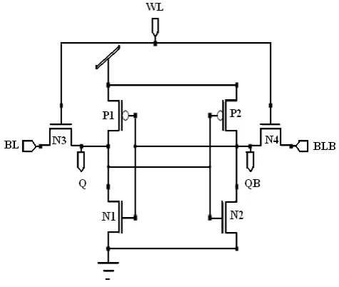
The conventional 6T memory cell comprised of two CMOS inverters cross coupled with two pass transistors connected to a complementary bit lines as shown in Figure 1. The gate of access transistors N3 and N4 are connected to the WL (word line) to have data written to the memory cell or read from the memory cell through the BL or BLB (bitlines) during write and read operation.
[image:1.595.319.557.452.653.2]The bit lines act as I/O buses which carry the data from the memory cell to the sense amplifier. Although it is not necessary to have two bit lines, both the signal and its inverse are typically provided in order to improve noise margins. SRAM cell perform three different operations, read, write and hold operation.
Fig 1: Conventional 6T SRAM Cell
3.
STATIC-NOISE-MARGIN (SNM)
Fig 2: The standard setup for SNM definition [6]
Figure 2 shows a common way of representing the SNM graphically for a bit-cell holding data. It plots the Voltage Transfer Characteristic (VTC) of Inverter 2 (inv2) and the inverse VTC-1 from Inverter 1(inv1). The resulting two-lobed curve is called a “butterfly curve” and is used to determine the SNM. The SNM is defined as the length of the side of the largest square that can be embedded inside the lobes of the butterfly curve.
Consider the case when the value of the noise sources with value Vn are introduced at each of the internal nodes in the bit cell. When the value of Vn increases from 0, this causes the VTC-1 for first inverter in Figure 2 to move downward and the VTC for the second inverter to move to the right. Once both move by the SNM value, the curves meet at only two points [3].
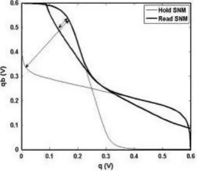
Fig 3: General SNM characteristics during Standby and Read operation
The resulting two-lobed curve is called as a “butterfly curve” as shown in Figure 3 and is used to determine the SNM. Values of SNM vary in different operation mode. SNM is becoming important factor to check the stability during read operation. It’s visible in Figure 3 that during read operation, the SNM takes its lowest value and the cell is in its weakest state.
The SRAM cell immunity to static noise is measured in terms of SNM that quantifies the maximum amount of voltage noise that can be tolerated at the cross-inverters output nodes without flipping the cell [4][5]. Any change in the noise, changes the value of the SNM during cell operation. Though the SNM is important during hold, cell stability during active
operation represents a more significant limitation to SRAM operation
.
3.1 Read Static-Noise-Margin
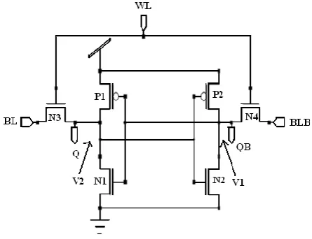
[image:2.595.321.524.169.341.2]The cell is most vulnerable when accessed during a read operation because it must retain its state in the presence of the bitline precharge voltage [7].
Fig 4: Equivalent SRAM Cell during Read operation
[image:2.595.73.266.380.547.2]If the cell is not designed properly, it may change its state during a read cycle which results in either a wrong data being read or a destructive read where the cell changes state. Thus, the worst noise margin is obtained during read access. Figure 4 shows the equivalent circuit during read operation.
Fig 5: Circuit used to measure read noise margin
The SNM is calculated when the word line is set high and both bit line are still precharged high. At the start of read access, the bit lines are precharged to Vdd and then the
wordlines are activated to access the cell. The node having the ‘0’ data pulls one of the bitlines to GND causing a voltage swing which is read by sensing circuits.
[image:2.595.333.521.457.613.2]dividing effect across the access transistor and drive transistor [8]. This increase in voltage severely degrades the SNM during the read operation.
The circuit for measuring the read margin is shown in Figure 5. One of the inverters is used and the bitline is connected to Vdd to simulate a read operation. A DC voltage sweep is
applied at node V1and the voltage at node V2 is measured to obtain the VTC.
4. DIFFICULTIES IN 6T SRAM CELL
The conventional 6T-cell schematic is shown in Figure 6. This most commonly used SRAM cell implementation has the advantage of very less area [9].
[image:3.595.331.534.272.409.2]However, the potential stability problem with this design arises during read and writes operation, where the cell is most vulnerable towards noise and thus the stability of the cell is affected. If the cell structure is not designed properly, it may change its state during read and write operation [10]. There are two types of noise margin which affects the Cell stability that are discussed shortly.
Fig 6: Voltage Stability Problem of 6T SRAM Cell
During the read operation, a stored “0” can be overwritten by a “1” when the voltage at node V1 reaches the Vth of nMOS N1 to pull node V2 down to
“0” and in turn pull node V1 up even further to “1” due to the mechanism of positive feedback. This results in wrong data being read or a destructive read when the cell changes state [11].
5. EXISTING 8T SRAM CELL
One of the major advantage of 8T SRAM cell is that data nodes are fully decoupled from read access and due to this the read stability is significantly improved. The conventional 6T SRAM cell is vulnerable to noise during the read operation, which when coupled with transistor mismatch( caused due to the process variation) could result in functional read failures. This cell shows poor stability at very small feature sizes, the hold and read static noise margins are small for robust operation. Therefore, an extensive literature can be found on
designing SRAM cells for low power operation in the deep sub-micron/nano ranges. The common approach to meet the objective of low power design is to add more transistors to the original 6T cell. An 8T cell can be found to solve the problem. This cell employs two more transistors to access the read bitline. The transistor configuration (i.e. M1 through M6) is identical to a conventional 6T SRAM cell. Two additional transistors M7 and M8 (thus yielding an 8T cell design) are employed in to reduce the leakage current.
[image:3.595.60.283.341.512.2]To overcome the problem of data storage destruction during the read operation, an 8T-cell implementation was proposed [12], for which separate read/write bit and word signal lines are used as shown in Figure 7, to separate the data retention element and the data output element. In turn, the cell implementation provides a read-disturb-free operation.
Fig 7: Existing 8T SRAM Cell
Write access to the cell occurs through the write access transistors and from the write bitlines, BL and BLB. Read access to the cell is through the read access transistor and controlled by the read wordline, RWL. The read bitline, RBL, is precharged prior to the read access. The wordline for read is also distinct from the write wordline. By doing this the worse-case stability condition encountered previously in a 6T SRAM cell, is avoided and high read stability is retained.
However, for the 8T structure, the read bitline leakage is greater, especially in deep submicron/nano ranges. When the column for Read (RBL) is not accessed, the leakage current through M7 may cause a severe voltage drop at the read bitline, leading to large Power dissipation, thus error may appear at the output. So we proposed another 8T SRAM Cell which can solve such kind of problems.
6. PROPOSED 8T SRAM CELL
stored node is connected to RBL. Thus a stored value at Q is being transferred to or read through RBL.
[image:4.595.319.538.104.170.2]One of the major advantage of this design is that it is not necessary to prepare a precharge circuit as required in prior 8T SRAM cell and a sense amplifier circuit as required in 6T SRAM cell because the stored value is directly passed through transmission gate. A charge/discharge power on the RBL is consumed only when the RBL is changed. Consequently, no power is dissipated on the RBL if an upcoming data is the same as the previous state. The design reduces a bitline power in both cases that the consecutive “0”s and consecutive “1”s are read out.
Fig 8: Proposed 8T SRAM Cell
7. SIMULATION RESULTS
All simulations have been performed on Tanner EDA tool version 12.6 using 45nm technology with input voltage ranging from 0.4V to 1V in steps of 0.2 V. In order to prove that proposed design shows better performance for Read-SNM, simulations are carried out for different voltages. To establish an impartial testing environment both circuits have been tested on the same input patterns which covers all the combination of input stream.
7.1 Power Consumption Analysis
The existing and proposed 8T have been simulated and checked for various parameters such as Power Consumption and Read-SNM. Table 1 shows that the power consumption of the SRAM designs increases with increasing supply voltage from 0.6V to 1V. The proposed 8T design of the SRAM Cell has remarkably less power consumption compared to the existing 8T SRAM design at various input voltages.
7.2 Read-Static-Noise-Margin Analysis
[image:4.595.57.282.243.376.2]The Read-SNM of the existing and the proposed 8T has been simulated for various Input voltages. The effect of Power Supply Voltage is important parameter which changes the cell stability during read mode and has been widely acceptable. It is preferable that the supply voltage must be maximum for increase SNM and also for cell stability.
Table 1. Power consumption vs. Supply voltage of existing 8T and proposed 8T SRAM
Different SRAM Cells
Power Consumption (uW)
0.6v 0.8v 1v
8T 0.20 0.76 1.57
Proposed 8T 0.078 0.24 0.43
[image:4.595.317.543.253.387.2]For this analysis, the supply voltage is varied from 0.4V to 1V. The noise margin for all operation is proportional to the supply voltage. The Read-SNM of the Proposed 8T is higher than the existing 8T SRAM Cell as shown by the Figure 9.
Fig 9: Read SNM vs. Power supply voltage of Existing and Proposed 8T SRAM
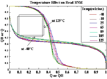
7.3 Temperature Analysis
The effect of temperature also plays a significant role on the noise margin of SRAM Cell. The SRAM Cell is used as a cache memory and thus the temperature ranges accordingly to the room temperature.
Fig 10: Effect of Temperature on read SNM
[image:4.595.321.540.515.677.2]given temperature range without altering the Read-SNM. The dimension of the square drawn inside the butterfly curve in Figure 10, is equal at -40°C and 125°C.
The effect of Temperature is almost insignificant on the Read-SNM of Proposed 8T SRAM Cell as shown by the results summarized in Figure 10 using temperatures -40°C,-10°C, 25°C,65°C,85°C,105°C and 125°C.
6. CONCLUSION
In this paper, a new 8T cell has been proposed to accomplish read stability and reduce bitline leakage problem, thus the proposed 8T can be used as a cache memory in internal CPU. It also maintains its Read-SNM at higher temperature range, thus it can be used in Industry and Military purposes also. So to overcome the Read-SNM problem encountered with conventional 6T SRAM cell and to avoid the bitline Leakage problem, we have proposed a method of introducing the effect of transmission gate so that these problems can be solved.
7. ACKNOWLEDGMENTS
The authors are very thankful to MITS (Deemed University) for providing a good laboratory facility. We simulate the result on Tanner EDA Tool version 12.6.
8. REFERENCES
[1] E. Seevinck et al., “Static-Noise Margin Analysis of MOS SRAM Cells,” IEEE J.Solid-State Circuits, vol.SC-22, no.5 pp.748-754, Oct. 1987.
[2] Benton H. Calhaun, Anantha P. Chandrakasan “Static Noise Margin Variation for Sub-threshold SRAM in 65 nm CMOS”, IEEE Journal of Solid-State Circuits,, pp.1673-1679. vol.41,July 2006.
[3] Benton H. Calhoun Anantha P. Chandrakasan, “Analyzing Static Noise Margin for Sub-threshold SRAM in 65nmCMOS”,ESSCIRC,2005.
[4] S. Tavva et al. “Variation Tolerant 9T SRAM Cell Design” GLSVLSI’10,pp.55-60,may 16, 2010.
[5] Arandilla,C.D.C et al.“Static Noise Margin of 6T SRAM Cell in 90-nm CMOS” IEEE 13th International Conference on computer modeling and Simulation, pp.534-539,March 30,2011.
[6] E. Grossar “Read Stability and Write-Ability Analysis of SRAM Cells for Nanometer Technologies”, IEEE J.Solid-State Circuits,vol.41,no.11 ,pp. 2577-2588,Nov. 2006.
[7] Sung Mo Kang and Yusuf Leblebici, “CMOS digital
integrated circuits-analysis and design,” Tata
McGraw-Hill, third edition, 2003.
[8] S. Nakata et al.,“Increasing Static Noise Margin of Single-bit-line SRAM Lowering Bit-line Voltage during Reading”.IEEE 54th International Midwest Symposium
on Circuits and Systems 2011.pp.1-4,7 Aug,2011. [9] K. Takeda et al., “A Read-Static-Noise-Margin- Free
SRAM Cell for Low-VDD and High-Speed Applications,” IEEE J.Solid-State Circuits,vol.41, no.1 pp.113-121, Jan., 2006.
[10]Do Anh-Tuan et al., “A 8T Diffrential SRAM With Improved Noise Margin for Bit-Interleaving in 65nm CMOS,” IEEE transactions on circuits and systems, vol.58, no.6,pp.1252-1263, June 2011.
[11]S.Birla et a.l.“Static Noise Margin Analysis of Various SRAM Topologies”IACSIT,pp.304-309,vol.3,No.3,june 2011.