A SURVEY ON DIFFERENT TECHNIQUES AND APPROACHES
FOR LOW POWER CONTENT-ADDRESSABLE MEMORY
ARCHITECTURES
V. V. Satyanarayana Satti and Sridevi Sriadibhatla
School of Electronics Engineering, Vellore Institute of Technology, Katpadi, Vellore, India E-Mail: [email protected]
ABSTRACT
This paper presents a survey on current trends adapted in the low power content addressable memory (CAM) architectures. CAMs are modified for the requirement of high speed, low power table look up function and are especially popular in network routers. CAM is a special type of memory with comparison circuitry. It stores or searches the look up table data with the help of one clock cycle. Large amount of power is consuming during comparison process because of parallel circuitry. CAM architectures are designed to reduce the power by eliminating the number of comparisons. In this paper at architectural level we survey different architectures for reducing dynamic power in CAM design. We reviewed seven different methods at the architectural level for low power.
Keywords: low power, precharge, short-circuits (SC) current, NAND cell, NOR cell.
1. INTRODUCTION
A content addressable memory (CAM) searches faster than algorithmic approaches and it is used for high speed search-intensive applications. CAM can be used in wide variety of applications including Huffman coding/decoding (Komoto et al., 1993), IP routing (Maurya et al., 2011), Data compression (Wei et al. 1993), Image processing (shin et al., 1992), Data management (Jalaleddine et al., 1999), Gray coding (Bremler-Barr et al., 2012), XML parsing (El-Hassan etal., 2011), Hough transformation (Nakanishi et al., 2000), internet protocol (IP) packets in network routers (Pei et al., 1991; Sun Y et al., 2012; Huang et al., 2001; Qin et al., 2002; Chao et al., 2002). In this paper we survey efficient methods for low power CAM design at the architecture level. First we briefly initiate the basic CAM operation. Then we present various methods in CAM design.
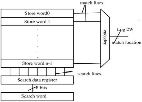
There are two types of CAM cells to store the digital data in the memory. First type of cell is binary content addressable memory (BCAM) which stores logic 0 or logic 1. Second type of cell is ternary content addressable memory (TCAM) which stores logic 0, logic 1 or logic X. TCAM adds a third state to CAM beyond binary for a wild card functionality that adds additional complexity to the circuit. Reading, writing and comparing are the three modes of operations in CAM to compare. Out of three compare operation is most important. To extract data residing on random access memory (RAM), the operating system provides the memory address where the data is stored. But the CAM function is almost opposite to that of RAM. Data stored in CAM can be accessed by search for the content itself and the memory retrieves the address of that content. The conventional CAM architecture (Schultz et al., 1997) consists of input search data register, search lines, match lines, array of CAM cells and encoder is shown in Figure-1. BCAM compares input search word to the table of stored data through the search lines and if match is found in the stored CAM word, it returns the address of the matching data to the encoder.
But in the case of TCAM more than one word may be matched. In this case word with longest prefix is selected and that address is returned to the priority encoder. If no match is found in any of the word, it flags the miss signal which is not shown in the architecture.
. . . . . . . Store word0
Store word 1
Store word n-1
Search data register
enc
od
er
match lines
search lines
Search word n bits
[image:1.595.309.543.400.569.2]match location Log 2W
Figure-1. Conventional CAM architecture.
1.1 CAM basic operation
The remaining content of the paper is structured as follows. In Section 2, we initiate with detailed description of CAM cells. Section 3 reviews different low power techniques at architectural level. Lastly, in section 4, we survey future trend for CAM research.
2. BASIC CAM CELLS
2.1. Binary CAM cells
BCAM is used for storing and searching fixed length table look up. A CAM cell can perform two basic tasks bit comparing and storing. There are two basic types of CAM cells binary NAND type and binary NOR type. In both type of CAM cells SRAM is used for storing bits. The bit comparison in both types of CAM cells is equivalent to XOR or XNOR of the stored bit and search bit and is implemented differently in each type.
2.1.1 Binary NOR CAM cell
In Binary NOR CAM cell, comparison between complementary search bit SL (SLB) and the store bit D
(DB) is performed with the help of four transistors C1, C2,
C3, and C4 is shown in Figure-2. These four transistors are typically minimum-sized to sustain high cell compactness. C1/C3 & C2/C4 are the two pairs of transistors which forms dual pull down paths for the match line ML separately. D and SL disables both pull down paths if there is match between stored bit and search bit which disconnects ML from ground. A miss match between D and SL enables at least one pull down path which connects match line ML to ground and hence ML discharges.
BCAM NOR cells are arranged in parallel to structure binary NOR match line ML. Figure-3 shows schematic of binary NOR match line with n cells. In NOR type BCAM searching for bits in the memory operates in three phases precharge search line, precharge match line and evaluating match line. High switching activity in NOR logic match line offers low search delay and high power consumption. Even in the evaluation of worst case NOR-cell is quicker than NAND. Power in a NOR CAM NOR-cell is reduced by minimizing match line capacitance, average switching activity and supply voltage. In each and every cycle of precharge, αl-1 match lines, each with match line capacitance CML have to be precharged. Power consumed
in a NOR match line is given by
PowerNOR = (αl -1) CMLV2DD (1)
NOR match line delay is given by
Delay NOR = TD+ tRC (2)
Where
TD = Delay of one transistor, TRC= Time constant of match
SL
ML
C1
C3 C4
C2
D DB
SLB
Figure-2. NOR-type CAM.
..
…
..
C1
C2
C3
C4
C1
C2
C3
C4
SL
B1SL
1SL
nSL
BnM
pree
D
BD
BD
D
ML
Figure-3. Schematic of a NOR match line with n cells.
2.1.2 Binary NAND CAM cell
Binary NAND CAM is shown in Figure-4. ND,
NDB and N1 are the three transistors used to compare search
bit SL (and SLB) and the store bit D (and DB). These three
transistors are typically minimum-sized to sustain high cell compactness. In the first case of matching SL=1 & D=1, the transistor ND is ON then it passes logic 1 to node X
which turns ON transistor N1. In the second case of
matching SL=0 & D=0, the transistor NDB is ON and it
passes logic 1 to node X which turns ON transistors N1.
Remaining all cases result in a miss condition. The pass transistors ND and NDB are OFF at that time. Both pass
transistors pass logic 0 to node B which turns OFF transistor N1. Hence node N1 is a pass transistor
implementation of XNOR operation of SL and D.
BCAM NAND cells are arranged in cascade to form a match line structure. Figure 5 shows schematic NAND cell match line with n cells. Searching for bits in NAND memory operates in two stages precharge of PMOS transistor Mpre, evaluation of NMOS transistor
Meval. During evaluation stage of NAND CAM cell, match
PowerNAND = CMLV2DD (3)
NAND match line delay of N transistor is given by
DelayNAND = N (TD+tRCseg) (4)
SL
D
D
BN
DN
DBN
1B
ML
nML
n+1SL
BFigure-4. NAND-type CAM.
……
..
N
1N
nD
1D
B1N
D1N
DB1N
DnN
DBneval
B
B
ML
M
preM
evale
SL
1SL
B1SL
nSL
BnML
0ML
1ML
n-1ML
n.
.
.
.
.
.
.
.
D
nD
BnMLSA
Figure-5. Schematic of a NAND match line with n cells.
3. POWER SAVING SCHEMES AT ARCHITECTURAL LEVEL
In this section we review different architectural techniques that are aimed at reducing the power in CAM. There is a large scope of power saving at architectural level and most of these techniques will reduce the total number of comparisons involved for a given searching operation and there by reducing the power consumption associated with larger parallel matching circuitry.
3.1 Bank selection
Bank selection scheme was discussed in (Lai et al., 2011; Motomura M et al., 1990; Schultz et al., 1994, Schultz et al., 1996). The aim of the above schemes was to save area. These schemes had been further modified to
BANK 0
BANK 1 BANK2 BANK3 Search data word
Decoder
11
Stored bits n-2 bits
[image:4.595.138.453.98.277.2]Bank selected bits (2bits)
Figure-6. Bank selection scheme.
The disadvantage of above scheme is increase in overflow. For example, consider a CAM with input search word which has 64 bits and two bank selection bits. CAM is divided into four banks for 24K entries. Each bank has 6K entries with 6K locations but actually 264 entries are possible per bank resulting in overflow. To overcome the problem of overflow, data bits in the different banks is balanced by time to time re-partitioning. Partitioning the binary data in the banks by developing algorithms to avoid overflow is an active area of research (Panigrahy, R. et al., 2002; Zane et al., 2003).
3.2 Precomputation
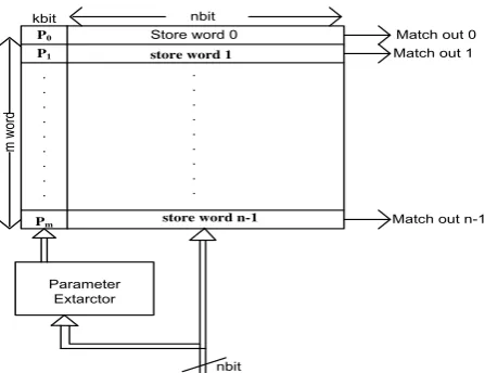
Another new CAM architecture is shown in Figure 7 for reducing dynamic power in CAM is precomputation-based CAM (CAM). Operation of PB-CAM depends on two blocks parameter memory & parameter extractor. Parameter extractor extracts factors from the input search word and it is then compared parallely to the factors stored in the parameter memory. If a match is formed in the parameter memory, the CAM words corresponding to those entries only compared with the input search word. This reduces the number of comparison operations involved. If no match is found, it indicates that input data mismatches with the data related to stored parameter. Hence a new parameter extractor has to be used in such case. One technique developed for PB-CAM parameter extractor is ones-count. This method is implemented with full adders. Ones-count PB-CAM fails in lowering the total number of comparison operations and it also consumes a huge quantity of power when the parameter value is between 5 and 9. Therefore to decrease the amount of similarity operations and power, a new parameter extractor called Block-XOR is proposed in (Ruan et al., 2008). This method required less association operations than the ones-count technique for parameter values between 5 and 9. One more PB-CAM method is
discrete uniform distribution into pre-computation block and reorder input data digits of the parameter extractor. It reduces average power consumption more than 60% when compared to GSEL algorithm.
store word 1
store word n-1
Parameter Extarctor P0
P1
Pm
nbit nbit
m w
ord
kbit
. . . . . . . . .
. . . . . . . . .
Match out 0 Match out 1
[image:4.595.311.535.357.529.2]Match out n-1 Store word 0
Figure-7. Block diagram of precomputation scheme.
3.3. Sparse clustered network
Sparse clustered network content addressable memory (SCN- CAM) consists of two blocks namely SCN based classifier and a special purpose CAM (Jarollahi et al., 2015). Figure 8 shows Block diagram of SCN-CAM. CAM in this architecture is separated into different sub blocks.
. .
. . . .
Miss
CAM Blk0
Data SRAM SCN
SCN-CAM
N N
N M
M
M×N M×S
q
CAM Blk M/ζ −1
. . . .
λ
Figure-8. Top level block diagram of SCN-CAM.
3.4 Selective match line energizer-CAM
CAM architectures reported in the literature so far had the source terminal of precharge transistors directly connected to supply voltage. But in the selective match line energizer (CAM) proposed in (Zackriya V.M & Kittur H.M., 2014). The architecture is divided in to two segments to reduce power, to improve search time and energy metric by selectively selecting the precharge. The view of SMLE-CAM architecture is shown in Figure 9. In this architecture word length in the memory is divided into two segments. In the first segment the first three bits of
SMLE-CAM architecture are constructed with match line energizer circuit. The match line energizer circuit uses modified XOR CAM cell and XNOR CAM cell and they form as sources for the precharge devices. The rest of the SMLE-CAM architecture is followed by NOR-CAM cell. In the second segment only match lines related to the word line are precharged whose first three bits are matched in the first segment. As searching is processed parallely in both the stages and precharge of match line is selectively performed, this design reduces power consumption and enhances the speed of searching operation.
Word 0
(0 to I bits)
Word 1
(0 to I bits)
Word m
(0 to I bits)
Word 0
(I to n bits)
Word 1
(I to n bits)
Word m
(I to n bits)
pre
pre
pre
ML
0ML
1ML
mData match
line 0
Data match
line 1
Data match
line m
.
.
.
.
.
.
.
.
.
.
Stage 1
Stage 2
Figure-9. Conceptual view of selective match line energizer CAM Architecture.
3.5 Hybrid CAM design
NOR type CAM consumes large power and provides best search performance because of short pull down paths. NAND type CAM is inefficient in searching but reduce power because of long pull down paths. Hybrid CAM is designed to use the advantage of both in (Chang Y.J & Liao Y.H., 2008). In this design word length of CAM is separated into two segments with a control circuitry in between is shown in Figure-10. In this circuit CAM segment 1 is constructed with XNOR type CAM
…..
….
……. ..
PRE
PRE
PRE XNOR CAM
CELL
XNOR CAM
CELL XOR CAM CELL
XOR CAM CELL
X1
X2
X3 K1
K2 K3
Y1
Y4
Y2 Y3
Z1 Z2
segment1 segment2
control
ML
Figure-10. Word structure of Hybrid CAM.
3.6 Early Predict and terminate miss matched match line in precharge
During precharge phase all the match lines initially charged to high. In evaluation phase, search input compares the data stored in the CAM. When there is a match, match line doesn’t drain the charge but it drains the charge in case of miss. As only one word matches with the input search word every time, current through the match lines of all the remaining miss matched words consume large power. To overcome this problem early predict and terminate precharge of match line is proposed in (Kittur H.M., 2017). The main objective is to terminate the mismatched ML early during precharge phase instead of charging all the match lines to full swing. This CAM
architecture is simple, but designed with effective precharge controller is shown in Figure-11. It varies precharge time dynamically to avoid precharging of miss matched ML to full level. Prd is a dynamically varying precharge signal and Pr is fixed width precharge signal. In precharge phase, when there is a match Prd is a replica of pre which makes match line to charge. When there is a miss Prdhalts the charging of ML as soon as the node MLp
reaches to threshold value of nMOS connected to the OR gate. This minimizes the unnecessary charging of the miss matching ML by at least 45- 55%. This CAM design is faster and report the efficient energy metric with reduced power.
n-bit search word length
p
r
i
o
r
i
t
y
e
n
c
o
d
e
r
………
.
………
..
…………
.
…………
.
…………
..
ML
1ML
nML
PML
kSL
1SL
1SL
nSL
n……
..
ML
kML
PP
1P
nPr
Pre charge controller
Pre charge controller
Pr
Pr
dPr
dFigure-11. Early predict mismatch of the ML to terminate the precharge.
3.7 Pre charge free CAM cell design
All CAM operations begin with precharging and are followed by evaluation. It is found that during precharge phase, CAM architecture is inefficient in
transistor. Suppose if there is a match in the first bit, ML0
goes high which in turn drives M0 into saturation region to
charge match line SML0. Similarly it continues for the
remaining bits till all the bits in that row are compared. If any of the bits mismatch let’s say third bit, then M2 moves
into cuts off that discharges match line SML2, and the
match line is connected to ground. Thus both control bit and pull down transistor reset the matchline to avoid short circuit current (Kittur, & H.M., 2016).
………..
. 8T CAM CELL
8T CAM CELL 8T CAM CELL SL
SL
bit bit
D D
ML0 ML1 ML2
CB Control bit
Match Line
SML0 SML1
Mb0
Mbn-1 Mb1
M0 M1 M2
Figure-12. Pre-charged free CAM cell.
4. FUTURE TRENDS IN CAM
The aim of any VLSI designers is to reduce area, performance and power. All the architectures developed in the above survey mainly concentrate on reducing dynamic power. As technology is scaling down design of low power architecture without sacrificing the performance is a challenging task. In deep submicron CMOS technology, leakage power is dissipated in standby mode, active mode and dominant over dynamic power. Future challenges in CAM designs are to reduce the leakage power not only in standby mode but also in active mode by applying some suitable low power techniques or by introducing novel architectures and technology traits.
5. CONCLUSIONS
In this paper detailed survey is performed on low power CAM architectures. First we initiated our discussion by brief introduction on CAM application, block diagram, architecture and power. We have reviewed binary NOR and NAND cells with their match line structures. CAM power reduction at the designing phase is clearly understood by reviewing the following seven architectures namely bank-selection, precomputation, sparse clustered network, SMLE, hybrid, early predict mismatched match line precharge and pre charge free.
REFERENCES
Bremler-Barr A. and Hendler D. 2012. Space-efficient TCAM-based classification using graycoding. IEEE Transactions on Computers. 61(1):18-30.
Chao H.J. 2002. Next generation routers. Proceedings of the IEEE. 90(9): 1518-1558.
Chang Y.J. and Liao, Y.H. 2008. Hybrid-type CAM design for both power and performance efficiency. IEEE Transactions on Very Large Scale Integration (VLSI) Systems. 16(8): 96: 965-974.
El-Hassan F. and Ionescu D. 2011. SCBXP: an efficient CAM-based XML parsing technique in hardware environments. IEEE Transactions on Parallel and Distributed Systems. 22(11): 1879-1887.
Hsieh J.Y. and Ruan S.J. 2008, March. Synthesis and design of parameter extractors for low-power pre-computation-based content-addressable memory using gate-block selection algorithm. In: Design Automation Conference, 2008. ASPDAC 2008. Asia and South Pacific. pp. 316-321.
Huang N.F., Chen W.E., Luo J.Y. and Chen J.M. 2001. Design of multi-field IPv6 packet classifiers using ternary CAMs. In: Global Telecommunications Conference, 2001 GLOBECOM '01. IEEE. 3: 1877-1881.
Jalaleddine S.M. 1999. Associative memories and processors: The exact match paradigm. Journal of King Saud University-Computer and Information Sciences. 11: 45-67.
networks. IEEE Transactions on Very Large Scale Integration (VLSI) Systems. 23(4): 642-653.
Kasai G., Takarabe Y., Furumi K. and Yoneda M. 2003, September. 200MHz/200MSPS 3.2 W at 1.5 V Vdd, 9.4 Mbits ternary CAM with new charge injection match detect circuits and bank selection scheme. In Custom Integrated Circuits Conference, 2003. Proceedings of the IEEE 2003 (pp. 387-390).
Kittur H.M. 2017. Content Addressable Memory-Early Predict and Terminate Precharge of Match-Line. IEEE Transactions on Very Large Scale Integration (VLSI) Systems. 25(1): 385-387.
Kittur H.M. 2016. Precharge-Free, Low-Power Content-Addressable Memory. IEEE Transactions on Very Large Scale Integration (VLSI) Systems. 24(8): 2614-2621.
Komoto E., Homma T. and Nakamura T. 1993, May. A high-speed and compact size JPEG Huffman decoder using CAM. In Symp. VLSI Circuits Dig. Tech. Papers (pp. 37-38).
Lai T.S., Peng C.H. and Lai F. 2011, March. Data driven approach for low-power pre-computation-based content addressable memory. In:Computers & Informatics (ISCI), 2011 IEEE Symposium on(pp. 328-333).
Maurya S.K. and Clark L.T. 2011. A dynamic longest prefix matching content addressable me mory for IP routing. IEEE Transactions on Very Large Scale Integration (VLSI) Systems. 19(6): 963-972.
Motomura M., et al. 1990. A 1.2-million transistor, 33 MHz, 20-bit dictionary search processor with a 160 kb CAM. Solid-State Circuits Conference, 1990. Digest of Technical Papers. 37th ISSCC. 1990 IEEE International. IEEE.
Nakanishi M. and Ogura T. 2000. Real-time CAM-based Hough transform algorithm and its evaluation. Machine Vision and Applications. 12(2): 59-68.
Pagiamtzis K. and Sheikholeslami A. 2006. Content-addressable memory (CAM) circuits and architectures: A tutorial and survey. IEEE Journal of Solid-State Circuits. 41(3): 712-727.
Panigrahy R. and Sharma S. 2002. Reducing TCAM power consumption and increasing throughput. InHigh Performance Interconnects, 2002. Proceedings. 10th Symposium on. pp. 107-112.
Pei T.B. and Zukowski C. 1991, April. VLSI
Qin G., Ata S., Oka I. and Fujiwara C. 2002, November. Effective bit selection methods for improving performance of packet classifications on IP routers. In: Global Tele communications Conference, 2002. GLOBECOM'02. IEEE. 3: 2350-2354.
Ruan S.J., Wu C.Y. and Hsieh J.Y. 2008. Low power design of precomputation-based content-addressable memory. IEEE Transactions on Very Large Scale Integration (VLSI) Systems. 16(3): 331-335.
Schultz K.J. 1997. Content-addressable memory core cells a survey. Integration, the VLSI journal. 23(2): 171-188.
Schultz K.J. and Gulak P.G. 1994, August. Fully-parallel multi-megabit integrated CAM/RAM design. In Memory Technology, Design and Testing, 1994, Records of the IEEE International Workshop on, (pp. 46-51).
Schultz K.J. and Gulak P.G. 1996. Fully parallel integrated CAM/RAM using to enable large capacities. IEEE Journal of Solid-State Circuits. 31(5): 689-699.
Shin Y.C., Sridhar R., Demjanenko V., Palumbo P.W. and Srihari S.N. 1992. A special- purpose content addressable memory chip for real-time image processing. IEEE Journal of Solid-State Circuits. 27(5): 737-7.
Sun Y., Egi N., Shi G. and Wu J. 2012, December. Content-based route lookup using CAMs. In: Global Communications Conference (GLOBECOM), 2012 IEEE (pp. 2677-2682).
Wei B.W., Tarver R., Kim J.S. and Ng K. 1993, May. A single chip Lempel-Ziv data compressor. In: Circuits and Systems, 1993. ISCAS'93, 1993 IEEE International Symposium on (pp.1 953-1955).
Zackriya V, M. and Kittur, H.M. 2014. Selective match-line energizer content addressable memory (SMLE-CAM). arXiv preprint arXiv:1406.7662.