A High Power Factor Supply Based on IBFC
Elizabeth Paul*, Prof. Aleyas M. V. **, Prof. Annie P. Oommen**
*Assistant professor, Dept of EEE, M. A. College of Engineering, Kothamangalam, India **Professor, Dept of EEE, M. A. College of Engineering, Kothamangalam, India **Professor, Dept of EEE, M. A. College of Engineering, Kothamangalam, India
Abstract- In recent years, power converters are used to get high power factor. This paper presents an integrated converter topology for driving HB LEDs which provides high power factor. The integrated buck flyback converter (IBFC) is a single stage, low cost, high power factor AC-DC converter with fast output regulation. The converter is used to provide power factor correction in streetlight application. To obtain high power factor, the buck stage and flyback stage are operated in discontinuous mode. Dimming operation of HB LED is also described. A closed loop is used for enabling the PWM dimming. The simulation studies using MATLAB/Simulink is also presented. Hardware setup of open loop is described.
Index Terms- HB LEDs, IBFC topology, ac/dc converter, DCM, power factor correction, single-stage, driver, PIC.
I. INTRODUCTION
ith the development of high brightness light emitting diode (HB LED) technology, the output light efficiency of power LEDs has increased over 100 lumens/W [1]. The HB LED can be used as a solid state light source in general lighting applications. In addition to high efficiency, it has no mercury content and has a longer life. In the future, the power LED is likely to replace the existing lighting sources like the incandescent lamp and fluorescent lamp.
In this paper, the main purpose is to present a topology for driving LED streetlight from an AC source. The important advantages of LEDs are reduced maintenance costs and high colour rendering index. Hence, colour reproduction is much better with LEDs than with LPSV lamps, since the latter emit only in the yellow wavelength. In addition, HB-LEDs do not exhibit either warm-up or restart periods, thus avoiding the need for extra control circuitry.
Since streetlights are powered from an AC source, they must comply with the International Electro technical Commission (IEC) 61000-3-2:2005 mandatory regulations in terms of harmonic content and power-factor correction (PFC) [2]. Additional requirements are that the electronic ballast must achieve high energy efficiency and be dimmable by pulse width modulation (PWM) technique. In general lighting applications, high power factor can be achieved using either a passive circuit or an active circuit [3], [4]. The passive circuit consist of inductors and capacitors together with uncontrolled rectifier. This is a good solution to achieve high power factor and does not generate electromagnetic interferences (EMI). However, it is difficult to achieve a higher power factor and lower THD with a passive PFC which uses only capacitors and inductors. Due to the presence of inductors and capacitors the size of the passive power correction circuit is large. So it is only suitable for low power applications.
In active power factor correction circuit, switch mode power supplies are used to achieve high power factor , low THD, and good output voltage regulation. Active power factor correction circuit is divided in to two categories, the two stage and single stage approaches. Single stage is the simplest active PFC circuit.
The most common single stage topologies used are the boost converter, the buck-boost, or buck-boost derived topologies. Block diagram representation of single stage power factor correction circuit is shown in Fig. 1. The single stage converter with PFC increases the stress on the switch in the converter due to input current and PFC voltage, and there is a power balance problem. Moreover, dimming of LEDs must be carried out at frequencies above 125Hz [5]. Therefore when dimming operation is required, these single stage solutions are not feasible.
Due to the above reasons, a two-stage converter is needed in order to perform PFC properly and to obtain a fast enough output dynamics. Block diagram of two stage power factor correction circuit is shown in Fig. 2. This system implementation consists of a PFC preregulator followed by a dc–dc converter in cascade. This scheme is usually implemented by means of a boost converter for the first stage and forward buck-boost-derived topologies or flyback converters for the output converter. In addition, even buck converters may be used for the former. These topologies are a very good solution, reaching unity power factor and providing fast output
dynamics. The disadvantage of two stage converters are high cost and size and the efficiency of the conversion is penalized because the output power is processed twice.
Input filter & rectifier
Converter for PFC and regulation
LED string
Controller AC
Co
D
C
i
n
p
u
t
[image:2.612.157.382.63.151.2]Vin
[image:2.612.183.429.178.312.2]Figure 1. Block diagram of single-stage power factor correction circuit
Figure 2. Block diagram of two stage power factor correction circuit
A good solution is to implement the so-called integrated single-stage (ISS) converters, which leads to the integration of the PFC stage together with the dc–dc converter [5]. This is achieved by eliminating one transistor and sharing the remaining transistor between the two stages. Block diagram of integrated single stage converter is shown in Fig. 3. These topologies are not only a good solution when HPF is needed but also can provide a fast output dynamics equivalent to that of two-stage PFC converters. In addition, the size of the whole converter is reduced, and therefore, the costs are reduced too. Moreover, the efficiency is usually very high in case of operation under narrow input-voltage-range conditions because part of the power is processed only once, or just a small part is processed twice within a single switching period.
Figure 3. Integrated single stage converter.
The integrated converter presented in this paper is composed of a buck converter working in DCM integrated with a DCM flyback dc–dc converter. The former is the PFC stage, whereas the latter supplies the power to the LED
lamp. Block diagram of IBFC is shown in fig. 4. The converter must be operated in DCM so that HPF can be achieved at the input, while the converter behaves as a current source at the output. The advantages of this topology over boost-based power factor pre-regulators lie in several main aspects. First, the bus voltage is much lower than that of boost or buck–boost based converters. Moreover, this dc bus voltage is not affected by duty cycle or input voltage variations. The bus voltage is depends only on the ratio between the buck and flyback inductances. Second, a lower dc bus voltage requires a lower voltage rating for the bulk capacitor, featuring a lower series equivalent resistance (ESR) device and longer life. Additionally, the buck converter features a natural
[image:2.612.190.428.426.564.2]Input filter & rectifier
Integrated buck flyback converter
LED string
Controller
AC Co
D
C
i
n
p
u
t
[image:3.612.193.431.62.160.2]Vin
Figure 4. Integrated single stage IBFC.
II. IDEAPRINCIPLEOFOPERATION
A. Circuit Description
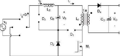
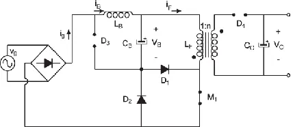
The integrated buck flyback converter is shown in Fig. 5. It consists of a buck converter and a flyback converter connected in series.
The circuit contains a buck inductor (LB), a bulk capacitor (CB), a switch (M1), flyback inductance (LF), output capacitor (C0), and
[image:3.612.188.426.275.380.2]diodes (D1, D2, D3 and D4).
Figure 5. Integrated buck flyback converter.
B. Circuit Operation
The operation of the IBFC is equivalent to two converters in cascade. The simplest way of operating the IBFC is maintaining the
DCM in both buck and flyback inductors. In this way, it will be demonstrated that the bulk capacitor voltage (VB) is independent of
load, duty cycle and switching frequency, and it only depends on the ac input voltage and the ratio of the two buck and flyback
inductances (LB and LF respectively). This is an important feature of integrated converters operating in DCM, which allows them to
provide fast output voltage regulation.
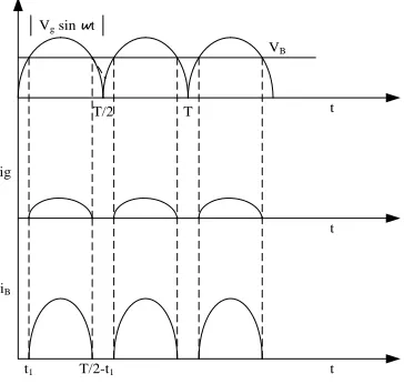
The operation of IBFC during a line half period has two modes.
Mode 1 (0 to t1): In the time intervals where the instantaneous line voltage is lower than the bulk capacitor voltage (vg<VB), the
rectifier bridge diodes are reverse biased and remain open. Thus, the buck inductance is not energized and diodes D1 and D3 are also
open during these time intervals. The equivalent circuit is shown in Fig. 6. In
this mode, only the flyback converter is operating through switch M1 and diodes D2 and D4. The operation is exactly equivalent to a
flyback converter, where the energy is taken from the bulk capacitor and delivered to the load.
Figure 6. Equivalent circuit of mode 1: vg< VB
Mode 2 (t1 to (T/2-t1)): In this mode, vg>VB.
In this interval, both buck and flyback inductors are energized when the control switch M1 is activated. Diodes D3 and D4 will remain
open and the currents through the buck and flyback inductors are handled by the integrated switch formed by M1, D1, and D4. Fig. 7
[image:3.612.207.410.550.646.2]Figure 7. Equivalent circuit of mode 2: vg>VB and M1 is ON
To understand how the currents are distributed among the three switches when M1 is ON, an equivalent circuit is shown in Fig. 8. In
this circuit, the switch M1 will handle the higher of the two currents iB and iF (buck and flyback currents, respectively). The diode in
parallel with the higher current will be open, whereas the diode in parallel with the lower current will be closed. Since the operation is in DCM, the two buck and flyback currents are ramp waveforms starting at the same instant. Therefore, the conclusion is that the
current through switch M1 will be either iB or iF, whichever is higher, but not the addition of the two currents. This is an advantage of
this converter compared to other integrated topologies, where the currents of the two stages circulate simultaneously through the control switch.
In summary, the current distribution is as follows. When iB > iF, current iB will circulate through M1, D1 will handle the current iB−
iF, with D2 being off. When iB < iF, current iF will circulate through M1, D2will handle the current iF− iB, with D1 being off.
M1
iF
iB
D1
[image:4.612.193.421.429.531.2]D2
Figure 8. Equivalent circuit during the conduction of M1
Figure 9. Equivalent circuit of mode 2: vg>VB and M1 is OFF
Fig. 9 shows the equivalent circuit of IBFC when M1 is OFF. During this interval, both buck and flyback inductors are being
de-energized and the energy is supplied to the bulk capacitor and load, respectively. In this stage, only diodes D3 and D4 will be
conducting as long as energy remains in the magnetic field of the buck and flyback inductors, respectively. The highest voltage across
the switch M1 (VM1) appears during this interval, can easily be calculated by using the equation (1)
Vg sin wt
VB
iB ig
t1 T/2-t1
T/2 T t
[image:5.612.215.397.66.239.2]t t
Figure 10. Input voltage and current waveform of IBFC
III. DESIGNEXAMPLEANDSIMULATIONSTUDIES
A. HB LEDs and Load Design
HB-LEDs are usually low-power devices, ranging from 1W to 5W at currents from 350 up to 2000 mA. At the present time, their luminous efficiency is around100 lm/W at 350 mA in the latest devices. The fact that they are low-power devices means that a large number of emitters will be necessary for wide-area-lighting applications such as streetlights.
The nominal power requirement for most LED streetlights
ranges from 60 to 150 W. The load finally chosen is made of ten Dragon Tapes running at 350 mA [6-9]. This gives a total of 60 LEDs emitting 1500 lm at 72 W. In order to properly design the power converter, the LED load has to be modeled.
B. Converter Design
The converter was designed to provide a total output power of 72 W, with a rated lamp current of 350 mA. In order to minimize the passive components, a 100-kHz switching frequency was selected.
C. Regulation and Dimming
Taking into account that HB-LEDs are current-controlled devices, a current control is preferable rather than a voltage control. Otherwise, slight changes in the string forward voltage would lead to great changes in the forward current. The flyback converter operating in DCM behaves as a current source, and therefore, an average current control can easily be performed.
PWM dimming can be carried out in three basic ways. The first, called “Series Dimming,” employs a series switch to interrupt the lamp current as commanded by the dimming signal. The main drawback of this solution is the high electrical stresses generated in the series switch. The second one, called “Shunt Dimming,” makes use of a switch in parallel to the load to divert the lamp current as commanded by the dimming signal. The main drawback of this solution is the dissipation of the energy stored in the output capacitor, which is sent to the parallel transistor, reducing the converter efficiency. The last, called “Enable Dimming,” is based on turning on and off the whole converter by means of an Enable/Disable input.
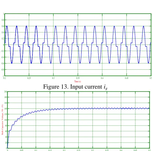
D. Simulation Results
Figure 11. Simulink model of open loop IBFC used for streetlight application
Figure 12. Input voltage vg
Figure 13. Input current ig
Figure 14. Bulk capacitor voltage VB
0.2 0.25 0.3 0.35 0.4 0.45 0.5
-400 -300 -200 -100 0 100 200 300 400 Time (s) I nput V ol ta ge ( V )
INPUT VOLTAGE (Vg = 230 Vrms)
0.2 0.25 0.3 0.35 0.4 0.45 0.5
-1 -0.8 -0.6 -0.4 -0.2 0 0.2 0.4 0.6 0.8 1 Time (s) I nput C ur r e nt ( A ) INPUT CURRENT
0 0.05 0.1 0.15 0.2 0.25 0.3 0.35 0.4 0.45 0.5
0 20 40 60 80 100 120 140 160 180 200 Time (s) B ul k C a pa c it or V ol ta ge , V b ( V )
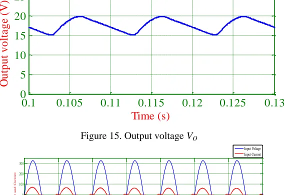
[image:6.612.184.430.377.621.2]Figure 15. Output voltage VO
Figure 16. Input voltage and current waveform
Figure 17. THD spectrum of input current
Figure 18. Simulink model of closed loop IBFC used for streetlight application
0.1
0.105
0.11
0.115
0.12
0.125
0.13
0
5
10
15
20
25
Time (s)
O
u
tp
u
t
v
o
lt
a
g
e
(
V
)
0.04 0.06 0.08 0.1 0.12 0.14 0.16 0.18
-300 -200 -100 0 100 200 300 Time (s) I nput V ol ta ge a nd C ur r e nt Input Voltage Input Current
-1 0 1 2 3 4 5 6 7 8 9 10
0 10 20 30 40 50 60 70 80 90 100 Harmonic order M a g ( % of F unda m e nt a l)
Figure 19. Input voltage and current of IBFC with closed loop
Figure 20. Output current of IBFC with closed loop
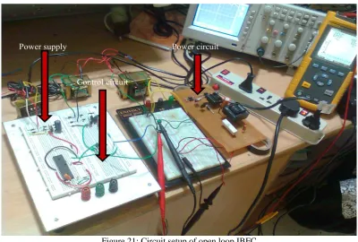
The circuit setup of open loop IBFC is shown in Fig. 21. It consists of controller unit, isolation and driver unit and power circuit module.
Figure 21: Circuit setup of open loop IBFC
The power circuit is fabricated in general PCB. Control circuit and power supply modules are setup in the bread board. Input voltage is 12 V, 50 Hz AC and the output is 17 V DC. The switching pulse of 100 kHz is generated using PIC microcontroller.
IV. CONCLUSION
The integrated buck flyback converter used to drive a string of LED is presented in this paper. The IBFC provides high power factor and fast output voltage regulation. It is proposed as a low cost solution for performing power factor correction in LED street lighting applications. A closed loop system for enabling dimming of LED is also discussed.
0.1 0.12 0.14 0.16 0.18 0.2 0.22 0.24 0.26 0.28 0.3
-300 -200 -100 0 100 200 300
Time (s)
I
nput
V
ol
ta
ge
a
nd
C
ur
r
e
nt
Input Voltage Input Current
2 2.01 2.02 2.03 2.04 2.05 2.06
0 0.05 0.1 0.15
Time (s)
O
ut
put
c
ur
r
e
nt
(
A
[image:8.612.106.506.338.608.2]REFERENCES
[1] B. Weir and F. Cathell, “LED streetlight demands smart power supply,” Power Electron. Technol., vol. 34, no. 2, pp. 34–39, Feb. 2008.
[2] J. M. Alonso, M. A. Dalla Costa, and C. Ordiz, “Integrated buck–flyback converter as a high-power-factor off-line power supply,” IEEE Trans. Ind. Electron., vol. 55, no. 3, pp. 1090–1100, Mar. 2008.
[3] K. Zhou, J. G. Zhang, S. Yuvarajan, and D. F. Weng, “Quasi-active power factor correction circuit for HB LED driver,” IEEE Trans. Power Electron., vol. 23, no. 3, pp. 1410–1415, May 2008.
[4] O. García, J. A. Cobos, R. Prieto, P. Alou, and J. Uceda, “Single phase power factor correction: A Survey”, IEEE Trans. PowerElectron., vol. 18, no. 3, pp 749-755, may 2003.
[5] D. Gacio, J. M. Alonso, A. J. Calleja, J. García, and M. R. Secades, ”A universal input single stage high power factor power supply for HB LEDs based on integrated buck flyback converter”, IEEE Trans. Ind. Electron., vol. 58,
no.2, pp 589-599, Feb. 2011.
[6] Luxeon K2 With TFFC, datasheet DS60, Jun. 2008. [7] “Diamond Dragon,” Datasheet LW W5AP (2008-05-15). [8] “Dragon Tape,” Datasheet OS-DT6 (2005-03-01). [9] “Golden Dragon,” Datasheet LW W5SG.
AUTHORS
Elizabeth Paul has completed her B. Tech in Electrical and Electronics Engineering from Sree Narayana College of Engineering,
kadayiruppu and M. Tech in Industrial Drives and Control from Rajiv Gandhi Institute of Technology, Kottayam. She currently holds the post of Assistant Professor in the Department of Electrical and Electronics, M. A. College of Engineering. Her email id is
Prof. Aleyas M. V. currently holds the post of Professor in the Department of Electrical and Electronics, M. A. College of
Engineering. His email id is [email protected].
Prof. Annie P. Oommen currently holds the post of Professor in the Department of Electrical and Electronics, M. A. College of