University of East London Institutional Repository:
http://roar.uel.ac.uk
This paper is made available online in accordance with publisher policies. Please
scroll down to view the document itself. Please refer to the repository record for this
item and our policy information available from the repository home page for further
information.
Author(s):
Lota, Jaswinder.
Article title:
Design of a Delta-Sigma (
Δ
-
Σ
) Based Digital-to-Analog Converter for
TETRA-2 Transmitter
Year of publication:
2010
Citation:
Lota, J. (2010) ‘Design of a Delta-Sigma (
Δ
-
Σ
) Based Digital-to-Analog
Converter for TETRA-2 Transmitter’ In: IEEE International Instrumentation &
Measurement Technology Conference, (IMTC 2010)
Austin Texas, USA, 03-06 May
Design of a Delta-Sigma (
Δ
-
Σ
) Based
Digital-to-Analog Converter for TETRA-2 Transmitter
Jaswinder Lota
Senior Member IEEE
School of Computing, IT & Engineering, University of East London London, United Kingdom
Abstract—This paper describes the design of a delta-sigma (Δ-Σ)
based Digital-to-Analog Converter (DAC) for a TETRA-2 transmitter along with the on-chip analog filtering to meet adjacent channel specifications. The proposed design meets the adjacent channel requirements with a margin of over 10 dB which is adequate to cater for hardware implementation. As the design specifications are in process of being finalised for TETRA-2, this paper will provide a valuable reference for designers involved with development of TETRA-2 radio equipment.
Keywords-delta-sigma (Δ-Σ); digital-to-analog converter (DAC); TETRA-2
I. INTRODUCTION
Terrestrial Trunked Radio (TETRA) [1] is a digital trunked mobile standard developed by the European Telecommunications Standards Institute (ETSI) [2]. The purpose of TETRA is to meet the Professional Mobile Radio (PMR) and Public Access Mobile Radio (PAMR) requirements. Some of the user organisations are public safety (fire, ambulance and rescue services), transportation, utilities (water and electricity) and government (police, border control and military). Like GSM moving to GPRS, EDGE and UMTS/3G, there was a requirement for it to evolve to satisfy increasing user demand for new services and facilities. In early 1999, interest groups comprising of both users and manufactures within the Technical Committee (TC) TETRA and TETRA Association (TETRAA) identified the need to enhance TETRA in several areas. At the end of 2005, this resulted in new standards being finalised as part of TETRA Release 2 [3]. The TETRA-2 Mobile Station (MS) uses Orthogonal Frequency Division Multiplex (OFDM) which is Time Division Multiple Access (TDMA) based capable of supporting channel bandwidths of 25 kHz, 50 kHz, 100 kHz and 150 kHz. The modulation schemes supported are pi/4-DQPSK, pi/8-DQPSK, 4-QAM, 16-QAM and 64-QAM. This paper pertains to the development of a Delta-Sigma (Δ-Σ) based Digital-to-Analog Converter (DAC) with the associated analog on-chip filtering for baseband processing of a TETRA-2 MS transmitter. Simulation results
indicate that the proposed design meets adjacent channel specifications with a margin of over 10 dB, which is considered adequate to cater for hardware implementation of the design.
As design specifications for TETRA-2 are in process of being finalised by ETSI, this paper will provide a valuable reference for designers involved with development of next generation TETRA-2 radio equipment. In Section II the baseband transmitter architecture is described. Section III describes the Δ-Σ DAC design and on-chip analog filtering. Simulation results are given in Section IV, followed by conclusions in Section V.
II. BASEBAND TRANSMITTER ARCHITECTURE
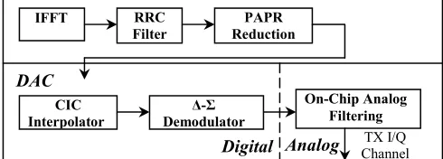
[image:2.612.314.559.559.647.2]The baseband transmitter is shown in Fig. 1. Inverse Fast Fourier Transform (IFFT) samples are filtered by the Root-Raised Cosine (RRC) filter [4], [5]. The Peak-to-Average Ratio (PAPR) of samples is then reduced by a PAPR reduction block, to a desired level to ensure linearity of Power Amplifier (PA) in the transmitter [6], [7]. Subsequent to PAPR samples are then fed to the Cascaded Integrator-Comb (CIC) interpolator at a higher sample rate than baseband Nyquist rate [8]. The samples in CIC interpolator are then up-sampled further and filtered. The samples are then converted to analog signal by a Δ-Σ demodulator. The last stage is the on-chip analog filtering required to ensure the required adjacent channel power levels are within the design specifications. The signal is then transmitted as in-phase/quadrature-phase (I/Q) analog component.
Fig. 1. Baseband transmitter architecture.
IFFT RRC
Filter
PAPR Reduction
CIC Interpolator
Δ-Σ Demodulator
On-Chip Analog Filtering
DAC
III. Δ-ΣDAC DESIGN
A. Δ-Σ DAC Sampling Rates
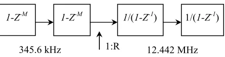
[image:3.612.315.557.186.353.2]This section describes the sampling rate for converting I/Q channel IFFT digital samples from Filter Bank to analog, capable of supporting various channel bandwidths required for TETRA-2. The symbol rate for TETRA-2 is 2400 Hz [3]. The 2400 Hz symbol rate is up-sampled by 144 in the filter bank to 345.6 kHz. Simulations confirm that 345.6 kHz is the minimum sample rate required to enable the CIC interpolator to ensure adequate adjacent channel attenuation for the widest channel bandwidth of 150 kHz. The CIC interpolator increases sample rate further by 36× to 12.442 MHz. The demodulator then converts the digital signal to analog at this high sample rate. The final on-chip stage is analog filtering that filters out high frequency quantization noise. The sampling rates are shown in Fig. 2.
Fig. 2. Δ-Σ DAC sampling rates.
B. CIC Interpolator
The interpolator is implemented as a CIC interpolator. It is an efficient implementation as no multipliers are required and there is no storage requirement for the filter coefficients. The structure consists of two basic building blocks i.e. differentiator and an integrator. The same filter design can easily be used for a wide range of up-sample rates. The transfer function of CIC interpolator is given by [8]:
( )
N RMz
z
z
H
−
−
=
−−11
1
(1)
where, R is the interpolation ratio (i.e. output frequency/input frequency), M is differential delay of the samples, which can be 1 or 2 and N is filter order. R is 36 giving the final sampling frequency of 12.442 MHz. A differential delay of M
=1 provides the filter cut off at 345.6 kHz for R=36. Although a higher value of N offers more attenuation, the droop at the band edge increases. The outermost sub-carrier for TETRA-2 in 150 kHz channel bandwidth (75 kHz I/Q bandwidth) is at 64.8 kHz [2]. N=3 is found adequate for filtering the high-frequency noise, offering a droop of -1.5 dB at 64.8 kHz. A 2nd-order CIC interpolator is shown in Fig. 3.
Fig. 3. CIC interpolator.
C. Δ-Σ Demodulator
A 3rd- order Δ-Σ demodulator topology is employed. A
[image:3.612.53.299.266.327.2]notch is added to the demodulator noise transfer function to place a noise-shaping zero at 114.4 kHz to reduce adjacent channel noise of the demodulator, by introducing a feedback factor α as shown in Fig. 4. The value of αwas found after a number of iterations in order to ensure that adjacent channel attenuation meets the required specifications. The demodulator coefficients are tabulated in tabulated Table I.
Fig. 4. Δ-Σ demodulator.
TABLE I.
α a1, a2 a3 a4 a5 a6 a7
0.0161 1.1 0.9 0.63 0.78 1.27 0.25
D. On-Chip Analog Filtering
This section describes on-chip analog filtering for the Σ-Δ DAC. The filtering is multistage as shown in Fig. 5. It consists of following three filters:
(a) 8th -order Bessel Filter
(b) 2nd -order Chebyshev Filter (a cascade of two 1st -order filters)
(c) 2nd-order Smoothening Filter
Fig. 5. On-chip analog filtering.
Since the overall design calls for a linear phase response, the type of analog filter family is limited. The appropriate choices would be Bessel, Linear Phase or Gaussian. An 8th
order Bessel filter with a linear phase response up to 259.2 kHz, i.e. 4 × 64.8 kHz (the maximum bandwidth) is found to
Filter
Bank CIC
Δ-Σ Demodulator
Analog Filtering
Up-sample
by 144 Up-sampleby 36
345.6 kHz 12.442 MHz
8th-order
Bessel Filter
1st-
order 1
st-
order
2nd-order
Chebyshev Filter
2nd-order
Smoothening Filter
1-Z-M 1/(1-Z-1) 1/(1-Z-1)
1-Z-M
1:R
[image:3.612.310.553.534.639.2] [image:3.612.70.292.643.700.2]meet the requirements. The filter response is shown in Fig. 6. The filter provides a linear phase in channel bandwidth up to 150 kHz and has an attenuation of –74 dB at 750 kHz.
Fig. 6. Bessel filter response.
The magnitude response in baseband droops to -0.63 dB at 64.8 kHz which along with the CIC droop needs to be compensated for prior in digital processing . A single Bessel filter is unable to provide adequate noise filtering in adjacent channels. A second order Chebyshev filter is therefore required for additional filtering. The filter can be a cascade of two 1st-order filters. Although it is an IIR filter, the phase
response in passband is linear because of low filter order. The droop at 64.8 kHz is -0.2 dB for the combination of two 1st
-order Chebyshev filters. This is followed by a 2nd-order
continuous-time filter with a cut-off frequency at 100 kHz. The filter requirements can be relaxed, as its main purpose is to smoothen the quantization noise from the previous stages.
IV. SIMULATION RESULTS
Simulations for the Δ-Σ DAC were undertaken in MATLAB. 1638400 FFT samples were measured with a Blackman window for various power spectrum measurements at different stages of the Δ-Σ DAC and adjacent channel performance was quantified.
A. Δ-Σ DAC Output
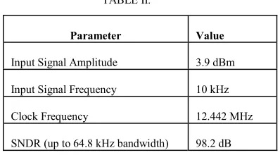
[image:4.612.337.536.318.428.2]The Δ-Σ demodulator output for a single-tone sinusoidal test signal is plotted in Fig.7 for which the performance parameters are tabulated in Table II. The input is at 3.9 dBm with frequency of 10 kHz. The clock frequency is 12.442 MHz. The Δ-Σ demodulator gives a Signal-to-Noise Distortion Ratio (SNDR) of 98.2 dB up to a baseband frequency of 64.8 kHz. The noise-shaping zero is observed at 114.4 kHz.
Fig. 7. Δ-Σ demodulator frequency resposne.
TABLE II.
Parameter Value
Input Signal Amplitude 3.9 dBm
Input Signal Frequency 10 kHz
Clock Frequency 12.442 MHz
SNDR (up to 64.8 kHz bandwidth) 98.2 dB
The CIC power spectrum output for a TETRA-2, 16-QAM 100 kHz channel bandwidth signal is shown in Fig. 8. The up-sampled signal spectrum is repeated with CIC interpolator offering noise adequate suppression in the adjacent channels.
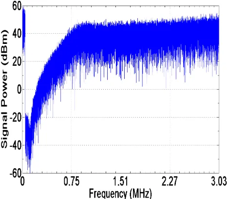
[image:4.612.318.546.498.700.2]The Δ-Σ demodulator output for the signal input in Fig. 8, is shown in Fig. 9. The Δ-Σ demodulator noise shaping is free from any spurious noise tones.
Fig. 9. Δ-Σ demodulator output spectrum.
The post analog filtering spectrum for the signal is plotted in Fig.10. The combination of Bessel filter with 2nd-order
Chebyshev filter and the 2nd-order smoothening filter offers
adequate noise supression for the Δ-Σ DAC. Noise
[image:5.612.57.284.469.696.2]suppression of more than 10 dB is achieved for all the channel bandwidths. This 10 dB margin is considered adequate the RF hardware implementation.
Fig. 10. Post analog filtering power spectrum.
B. Δ-Σ DAC Adjacent Channel Performance
The adjacent channel specifications for transmission of TETRA-2 are given in [3]. The output of Δ-Σ DAC is at least 10 dB below these specifications for all the channel bandwidths. The Σ-Δ DAC noise levels for the 100 kHz channel bandwidth are tabulated in this section.
1) Impact of unwanted emissions near to the carrier
The specifications relate to the impact of unwanted emissions near the carrier on the coexistence of a TETRA-2 system with other analog or digital systems [3]. It concentrates on the interference in the channel(s) adjacent to the active channels. The specifications along with the Δ-Σ DAC quantization noise-levels measured from simulations are given in Table III.
TABLE III.
Frequency Offset
Specified Level MS Nominal Power
3W
Δ-Σ DAC Noise-level
87.5 kHz -55 dBc -67dBc
112.5 kHz -60dBc -71 dBc
137.5 kHz -60 dBc -75dBc
2) Impact of unwanted emissions far from the carrier
The specifications relate to the impact of unwanted emissions far from the carrier on coexistence of a TETRA-2 system with other systems [3]. It concentrates on interference due to wide-band noise like emissions, which have a much lower level than the adjacent channel power but potentially affect a larger number of channels. These limits apply to emissions within the transmit band of TETRA-2 transmitter, within the TETRA-2 receive bands and beyond the TETRA-2
allocation, where f denotes the frequency offset
corresponding to the near edge of the receive band. The specifications along with the Δ-Σ DAC quantization noise-levels measured from simulations are given in Table IV.
TABLE IV.
Frequency Offset
Specified Level MS Nominal Power
3W
Δ-Σ DAC Noise-levels
162.5-312.5 kHz -60 dBc -76 dBc
312.5-562.5 kHz -63 dBc -132 dBc
562.5-1500 kHz -73 dBc -137 dBc
1500 kHz-f -73 dBc -137 dBc
V. CONCLUSIONS
Design of a Δ-Σ based DAC along with the on-chip analog filtering for a TETRA-2 MS transmitter is given in this paper. Simulation results indicate that the Δ-Σ DAC quantization noise-levels are at least 10 dB below the required specifications for all the TETRA-2 bandwidths. This 10 dB margin is considered adequate to cater for the circuit non-idealities and RF implementation.
REFERENCES
[1] Terrestial Trunked Radio (TETRA) Communication. Available at: www.tetramou.com
[2] Eurpoean Telecommunications Standards Institute. Available at: www.etsi.org
[3] ETSI Standards TR 102 580 V1.1.1 Terrestrial Trunked Radio (TETRA); Release 2; Designer's Guide; TETRA High-Speed, Data (HSD); TETRA Enhanced Data Service (TEDS) Trunked Radio.
[4] R. V. Nee and R. Prasad, OFDM for Wireless Multimedia
Communications, Artech House, 2000.
[5] John A, C. Bingham, “Multicarrier modulation for data transmission: An idea whose time has come,” IEEE Communications Magazine., vol. 28, , May 1990, pp. 5-14.
[6] S. H. Han And J. H. Lee, “An overview of peak-to-average power ratio reduction techniques for multicarrier transmission” IEEE Wireless Comm., vol. 12, April, 2005, pp. 56-65.
[7] Elena Costa, et al, “Impact of amplifier nonlinearities on OFDM transmission system performance ” IEEE Comm. Lett., vol. 3, Feburary 1999, pp. 37-39.