Threshold Voltage Sensitivity to Metal Gate
Work-Function Based Performance Evaluation of
Double-Gate n-FinFET Structures for LSTP Technology
M. Mustafa1, Tawseef A. Bhat2*, M. R. Beigh2
1Guru Nanak Institute of Engineering and Management, Naushera Hoshiarpur, Punjab, India 2Department of Electronics & Instrumentation Technology, University of Kashmir, Srinagar, India
Email: *[email protected]
Received February 2,2013; revised March 8, 2013; accepted March 16,2013
ABSTRACT
This paper investigates the threshold voltage sensitivity to metal gate work-function for n-channel double gate fin field-effect transistor (FinFET) structures and evaluates the short channel performance of the device using threshold voltage dependence on metal gate work-function analysis. We carried out the study for a double gate n-channel fin field-effect transistor (n-FinFET) with parameters as per the projection report of International Technology Roadmap for Semiconductors, ITRS-2011 for low standby power (LSTP) 20 nm gate length technology node. In the present study device simulation have been carried out using PADRE simulator from MuGFET, which is based on the drift-diffusion theory. Our results show the accuracy and validity of classical drift-diffusion simulation results for transistor structures with lateral dimensions 10nm and above. The subthreshold behavior of device improves with increased metal gate work-function. The results also show that a higher gate work-function (≥5 eV) can fulfill the tolerable off-current as projected in ITRS 2011 report. The SCE in FinFET can reasonably be controlled and improved by proper adjustment of the metal gate work-function. DIBL is reduced with the increase in gate work function.
Keywords: FinFET; DIBL; SS; Threshold Voltage; SCE’s
1. Introduction
The continuous downscaling of MOS device has re- mained imperative need for the aggressive increase in transistor density and performance, leading to efficient chip functionality at higher speeds. As the conventional single gate planar transistor dimensions are scaled down in order to meet the requirements of International Tech- nology Roadmap for Semiconductors (ITRS) projec- tions [1] for semiconductor device scaling, various SCE’s become too severe, fabrication cost increases and process of the devices becomes increasingly difficult. The challenges of continuous device scaling have been solved by incorporating advanced multi-gate MOS de- vice structures such as fin field-effect transistors (Fin- FETs) [2,3], which utilize two or more gate electrodes and an ultrathin body. These devices have shown excel- lent device performance at aggressively scaled device parameters. FinFET technology has became very much attractive for device designers and researchers to look for efficient structural and process parameters in these de- vices, leading to a diversified research in such novel de- vice structures.
A very important aspect regarding the FinFET struc- tures is the threshold voltage tuning and its sensitivity to different device parameters. A study was carried out on the sensitivity of threshold voltage to channel doping density in extremely scaled MOSFET structures [4]. In the study it has been found that threshold voltage is, in fact, insensitive to doping variation over a wide range of doping density and such insensitivity is further extended by bandgap narrowing in nanoscale MOSFET structures. Device simulations carried out by S. Xiong et al. in [5]
has shown that threshold voltage is insensitive to channel doping below 1 × 1019 cm−3. A higher channel doping
requirement for the adjustment of threshold voltage may affect the channel mobility of carriers. Further, due to random and discrete nature of dopant atoms, the same macroscopic doping profiles differ microscopically. Thus, engineering the work function of gate materials and maintaining a nearly intrinsic channel has been found more desirable. A method to suppress the earlier conduc- tion of the corners in the bulk-FinFETs and to achieve a reasonable threshold voltage control with low leakage currents, without increasing the body doping has been proposed by K.-R. Han, et al. [6]. It has been observed
that by increasing the top gate work-function at a fixed side gate work-function of bulk FinFET, threshold volt- age increases and off-state leakage current (Ioff) reduces
significantly without increasing doping concentration of fin body. Classical device simulations carried out using Silvaco PISCES in [7] suggest that the optimal gate work-function is such that the gate Fermi level is 0.2 eV below (above) the conduction (valence) band edge. Mid- gap gates have been found inefficient because of severe SCE’s. Among the logic technology of MOSFET de- vices, the low standby power (LSTP) logic technology refers to chips of lower-performance, lower-cost con- sumer type applications, such as consumer cellular tele- phones, with lower battery capacity and an emphasis on the lowest possible static power dissipation, i.e., the
lowest possible leakage or off-current (highest threshold voltage, Vt). There are difficult challenges to keep the
leakage current within tolerable range as predicted by ITRS, while at the same time maintaining a higher thres- hold voltage requirement in these device structures. Ad- justment of threshold voltage through gate work function engineering rather than through channel doping is very efficient because of the limitations imposed on the cur- rent drive and mobility in short channel and ultrathin MOS devices. Controlling and improving the SCE’s in FinFET by adjustment of the metal gate work-function provides an alternative method over controlling it either by reduction in fin height and fin thickness.
Both poly-silicon and metals have been utilized as gate materials since the evolution of MOS transistor device structures. The aggressive scaling of metal-oxide-semi- conductor (MOS) devices requires the implementation of a metal gate in place of conventional polycrystalline silicon. It is because poly-gate devices show a high gate resistance, dopant penetration to channel region and an increase in equivalent oxide thickness (EOT) due to poly-Si depletion [8]. Metal gates have been found at- tractive compared to poly-silicon gates since early 1990’s due to their chemical stability with the high-k gate di- electric materials. Furthermore, it is possible to maintain higher threshold voltages by tuning to a suitable higher metal gate work function while at the same time acquir- ing high gate stack stability [9-12]. The authors in this paper reported about the sensitivity of threshold voltage in case of n-channel double gate FinFET structures to metal gate work-function and investigates the effect of various SCE’s on the device performance while at the same time takes care of the required tolerable limit of leakage current (Ioff) value as predicted by ITRS [1]. A
detailed and systematic study of the performance evalua- tion of the FinFET devices based on the metal gate work-function dependence of the threshold voltage as to exploit these devices to highest application has been the main aim of the present work and presented in this paper.
2. Threshold Voltage Variation and Gate
Work-Function Engineering
The threshold voltage expression in case of a MuGFET device structure can be expressed as [13]
2 D SS
t ms f
ox ox
Q Q
V f f V
C C in
(1)
where Qss represents charge in the gate dielectric, Cox is
the gate capacitance, QD is the depletion charge in the
channel, fmsrepresents metal-semiconductor work-func
tion difference between the gate electrode and the semi- conductor, ff is the fermi potential which for P-type sili-
con is given by
ln A f i N kT f q n
(2)
where NA is acceptor concentration and ni is intrinsic
carrier concentration.
For ultrathin body and lightly doped devices the effect of QD and Qss on threshold voltage, Vt in Equation (1) is
negligible compared to ff. Further Vinis the additional
surface potential to 2ff that is needed for ultrathin body
devices to bring enough inversion charges in to the channel region of the transistor to reach threshold point. Therefore, the work-function of gate electrode is the main parameter for threshold voltage determination in case of MuGFET devices.
3. Device Structure and Simulation Strategy
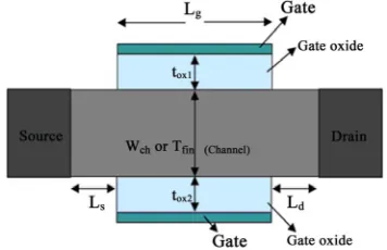
A 2-D view of device structure of FinFET used in the present simulation work is as shown in Figure 1, speci-fying various device parameters undertaken for simula- tion study.
The critical geometrical parameters of the FinFET are defined as below:
1) Lg: the channel length or gate length is the final as
etched length at the bottom of the gate electrode.
2) Wch: the channel width is defined as the separation
[image:2.595.334.512.605.720.2]between the two side wall or lateral gates on either side of the fin. Other nomenclatures used for channel width are fin width or fin thickness.
3) tox1, tox2: thickness of the oxide material placed on
the either side walls of fin before a gate contact is made. 4) Ls, Ld: extension lengths to source and drain and
determine the critical source/drain resistance and capaci- tance of device.
The various parameter values of the device structure undertaken for the present study are as per the projection report of ITRS-2011 update for LSTP technology, an- ticipated for the year 2015 [1]. Some of the parameters are also user defined. These parameters of FinFET struc- ture are as listed in the Table 1.
In the present study, device simulations have been car- ried out using PADRE simulator from MuGFET [14], which is based on the drift-diffusion simulation. The drift-diffusion is being utilized for the device simulation, because of the fact that subthreshold characteristics of device are still diffusion dominated and reflect device characteristics in the subthreshold region and other re- sults are reasonably well in consonance with the experi- mental results [15,16]. The drift-diffusion simulator is way faster than the quantum transport simulator that pro- vides physical insight of the device. The quantum me- chanical effects become negligible while simulating the transistor structures with lateral dimensions greater than 10nm. A comparison of experimental results obtained in [17] for the subthreshold Id-Vg characteristics with the
simulation results using MuGFET simulator has been given in [15], which clearly indicates the accuracy and validity of classical drift diffusion simulation results.
4. Simulation Results
4.1. Threshold Voltage Variation with Metal Gate Work Function
[image:3.595.316.529.393.526.2]Since the work function of the metal gate can be tuned to meet a given threshold voltage requirement, the choice of the material to be used for the metal gate in such devices
Table 1. Device parameters undertaken for the simulation study.
Device parameters Values undertaken
Physical Gate Length (Lg) 20 nm
Equivalent Oxide Thickness
(EOT or tox1, tox2) 1.2 nm
Vdd (Power Supply Voltage) 0.86 V
Fin width (Wch) 12.5 nm
Channel Dopinga 4 × 1018 cm−3
Drain/Source Dopinga 1 × 1021 cm−3
Isd,leakage 10 p A/µm
Extension length to Source /Drain (Ls & Ld)a 30 nm
aUser defined values.
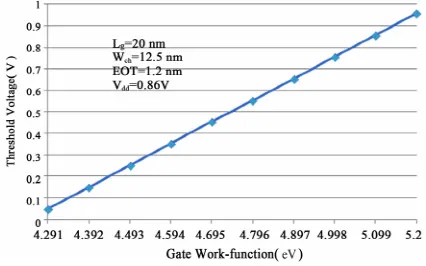
willdepend on that which of the metal provides the work function suited for given threshold voltage accomplish- ment. MOS transistors fabricated using Mo (Molebidi- num) gate have been reported to have a gate work-func- tion value of 5 eV [11]. We investigated the variation of threshold voltage, Vt for the gate work function ranging
from 4.291 to 5.2 eV in the present simulation study. It has been found that by increasing the gate work-function of FinFET, the corresponding threshold voltage increases to a desired value as depicted in Figure 2 The metal gate
work-function dependence of the threshold voltage comes out to be linear relation, which can be also verified through the Equation (1). The results as depicted in this figure have been obtained for a device having Lg = 20 nm,
Wch = 12.5 nm, EOT = 1.2 nm and Vdd = 0.86 V.
Main-taining higher threshold voltage is a key requirement for LSTP logic technologies and hence can be achieved more efficiently by increasing work-function of the metal gate material.
4.2. Transfer Characteristics
Figure 3 shows the variation of drain current, Ids versus
gate voltage, Vgs characteristics of FinFET for different
[image:3.595.59.286.568.721.2]values of gate work-function. The metal gate work-
Figure 2. Threshold voltage versus gate work-function of n-FinFET.
[image:3.595.313.532.573.708.2]function has been varied from 4.392 eV to 5.2 eV. The results depict that the subthreshold behaviour of device improves as the metal gate work-function is increased to higher values. It is because of the fact that as the in- crease in metal gate work-function increases the corre- sponding threshold voltage, which in turn reduces the off-state leakage current and results in the improvement in the device performance. This is very enviable charac- teristics of the device for LSTP applications.
4.3. On-Current
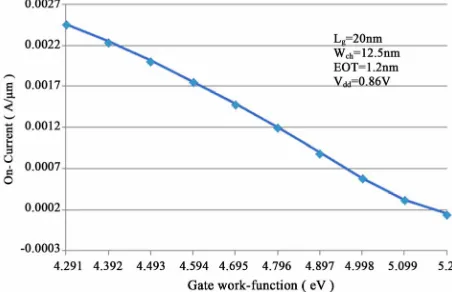
The device on-current behaviour as a function of gate work-function has been illustrated in Figure 4. It is clear
that device on-current is sacrificed for increased thresh- old voltage with increase in metal gate work-function of FinFET structure.
4.4. Off-Current
[image:4.595.59.285.389.535.2]For LSTP technology logic application, the off-state leakage current requirement as projected by the ITRS 2011 report is of the order of 10 p A/µm at room tem- perature. It is clear from the off-state device charac- teristics shown in Figure 5 that a higher gate work-
[image:4.595.311.536.389.537.2]Figure 4. On-current versus gate work-function of n-FinFET.
Figure 5. Off-current versus gate work-function of n-FinFET.
function approximately 5 eV can fulfil this tolerable off- current projection of the given FinFET structure.
4.5. On-Off Current Ratio
As shown in Figure 6, the on/off current ratio obtained
from the device simulations has been found to improve significantly with the increase in metal gate work-func- tion of FinFET. Although the device on current reduces to some extent with an increase in gate work-function, but an increase in on-off current ratio is a clear indication of overall improvement in drive current with a required low off-state leakage current for LSTP logic technology.
4.6. Drain Induced Barrier Lowering (DIBL)
DIBL is one of the critical short channel effect parameter of nanoscale device structures, since it estimates the overall gate control of the device on the channel electro- statics of the device. The effect of DIBL is to reduce the threshold voltage in nanoscale MOS devices due to a modulation of the source to drain channel potential bar- rier by the drain voltage to make the conduction of de- vice channel possible for smaller gate voltages. From
[image:4.595.59.284.566.721.2]Figure 7, it is clear that DIBL gets reduced with the
Figure 6. On-off current ratio versus gate work-function of n-FinFET.
[image:4.595.311.533.580.721.2]Figure 8. Subthreshold slope versus gate work-function of n-FinFET.
increase in gate work function. It is because with in- crease in threshold voltage due to increased gate work- function, barrier lowering effect is reduced for a given drain source voltage in short channel FinFET devices.
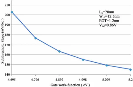
4.7. Subthreshold Slope
The plot of subthreshold slope versus gate work-function of FinFET is as shown in Figure 8. It is clear that sub-
threshold slope of given FinFET structure improves with the increase in gate work-function of the device. The improved SS characteristic is as a result of increased de- vice threshold voltage.
5. Conclusion
The study presents the effectiveness of gate work-func- tion engineering for the adjustment of threshold voltage in nanoscale FinFET structures. Utilization of metal gates have been proposed for nanoscale FinFET devices due to their capability to withstand high-k gate dielectric materials that are very much essential for the continuous downscaling of device structures. The efficiency of util- izing metal gates has been presented by studying the threshold voltage in FinFETs with respect to metal gate work-function. An analysis based on the evaluation of corresponding SCE’s and device performance has been presented that supports utilization of metal gate work- function performance for such devices to be used for LSTP logic technology applications. During the simula- tion study, it has been observed that engineering thresh- old voltage through variation of metal gate work-func- tion of FinFET can produce FinFETs that may have re- duced SCE’s and higher device performance. Varying the device gate work-function is found effective in ad- justing the threshold voltage to a desired value. The SCE in FinFET can reasonably be controlled and improved by proper adjustment of the metal gate work-function. The increased gate work-function improves the DIBL, SS, Off-current, On/Off current ratio, but causes a reduction
in device On-current.
REFERENCES
[1] “International Technology Roadmap for Semiconduc- tors,” 2011. http://www.itrs.net
[2] D. Hisamoto, T. Kaga, Y. Kawamo and E. Takeda, “A Fully Depleted Lean-Channel Transistor (DELTA)—A Novel Vertical Ultra Thin SOI MOSFET,” Technical Di- gest of IEDM,Washington DC, 3-6 December 1989, pp.
833-836
[3] D. Hisamoto, W. C. Lee, J. Kedzierski, H. Takeuchi, K. Asano, C. Kuo, E. Anderson, T. J. King, J. Bokor and C. M. Hu, “FinFET—A Self-Aligned Double-Gate MOS- FET Scalable to 20 nm,” IEEE Transactions on Electron Devices, Vol. 47, No. 12, 2000, pp. 2320-2325.
doi:10.1109/16.887014
[4] M.-H. Chiang, C.-N. Lin and G.-S. Lin, “Threshold Volt- age Sensitivity to Doping Density in Extremely Scaled MOSFETs,” Semiconductor Science and Technology, Vol.
21, No. 2, 2006, pp. 190-193. doi:10.1088/0268-1242/21/2/017
[5] S. Xiong and J. Bokor, “Sensitivity of Double-Gate and
FinFET Devices to Process Variations,” IEEE Transac- tions on Electron Devices, Vol. 50, No. 11, 2003, pp.
2255-2260. doi:10.1109/TED.2003.818594
[6] K.-R. Han, B.-K. Choi, H.-I. Kwoni and J.-H. Lee, “De- sign of Bulk Fin-Type Field-Effect Transistor Consider- ing Gate Work-Function,” Japanese Journal of Applied Physics, Vol. 47, No. 6, 2008, pp. 4385-4391.
doi:10.1143/JJAP.47.4385
[7] I. De, D. Johri, A. Srivastava and C. M. Osburn, “Impact of Gate Workfunction on Device Performance at the 50 nm Technology Node,” Solid-State Electronics, Vol. 44,
No. 6, 2000, pp. 1077-1080. doi:10.1016/S0038-1101(99)00323-8
[8] C. J. Choi, M. Y. Jang, Y. Y. Kim, M. S. Jun, T. Y. Kim, B. C. Park, S. J. Lee, H. D. Yang, R. J. Jung, M. Chang, and H. S. Hwang, “Effective Metal Work Function of High-Pressure Hydrogen Postannealed Pt-Er Alloy Metal Gate on HfO2Film,” Japanese Journal of Applied Phys-
ics,Vol. 46, No. 1, 2007, pp. 125-127.
doi:10.1143/JJAP.46.125
[9] R. J. P. Lander, J. C. Hooker, J. P. van Zijl, F. Rooze- boom, M. P. M. Maas, Y. Tamminga and R. A. M. Wolt- ers, “A Tuneable Metal Gate Work Function Using Solid State Diffusion of Nitrogen,” ESSDERC, Florence, 24-26 September 2002, pp. 103-106.
[10] M. C. Lemme, J. K. Efavi, H. D. B. Gottlob, T. Mollen- hauer, T. Wahlbrink and H. Kurz, “Comparison of Metal Gate Electrodes on MOCVD HfO2,” Microelectronics
Reliability, Vol. 45, No. 5-6, 2005, pp. 953-956.
doi:10.1016/j.microrel.2004.11.018
[11] R. Lin, Q. Lu, P. Ranade, T.-J. King and C. M. Hu, “An Adjustable Work Function Technology Using Mo Gate for CMOS Devices,” IEEE Electron Device Letters, Vol.
23, No. 1, 2002, pp. 49-51. doi:10.1109/55.974809
CMOS Devices,” Ph.D. Dissertation, Uppsala University, Uppsala, 2006.
[13] J.-P. Collinge, “FinFET and Other Multi-Gate Transis- tors,” Springer, Berlin, 2008.
doi:10.1007/978-0-387-71752-4
[14] “MuGFET v 1.1, Simulation tool for Nanoscale Mul- tigate-FET Structures (FinFET and Nanowire).”
http://www.nanohub.org
[15] “First Time User Guide (FTUG) to MuGFET v 1.1.”
https://nanohub.org/tools/MuGFET/FTUG
[16] T.-S. Park, E. J. Yoon and J.-H. Lee, “A 40 nm Body- Tied FinFET (OMEGA MOSFET) Using Bulk Si Wa- fer,” Physica E: Low-Dimensional Systems and Nanos- tructures, Vol. 19, No. 1-2, 2003, pp. 6-12.
[17] Y.-K. Choi, T.-J. King and C. M. Hu, “Nanoscale CMOS Spacer FinFET for the Terabit Era,” IEEE Electron De- vice Letters, Vol. 23, No. 1, 2002. pp. 25-27.