SN74LS125A, SN74LS126A
Quad 3-State Buffers
LS125A
14 13 12 11 10 9
1 2 3 4 5 6
VCC
8
7 GND
E D O E D O
D O
E D O E
LS126A
14 13 12 11 10 9
1 2 3 4 5 6
VCC
8
7 GND
E D O E D O
D O
E D O E
TRUTH TABLES
LS125A LS126A
INPUTS INPUTS
E D OUTPUT E D OUTPUT
L L L H L L
L H H H H H
H X (Z) L X (Z)
L = LOW Voltage Level H = HIGH Voltage Level X = Don’t Care
(Z) = High Impedance (off)
GUARANTEED OPERATING RANGES
Symbol Parameter Min Typ Max Unit
LOW
POWER
SCHOTTKY
SOIC D SUFFIX CASE 751A
PLASTIC N SUFFIX CASE 646
14 1
14 1
SOEIAJ M SUFFIX CASE 965
14 1
Device Package Shipping
ORDERING INFORMATION
SN74LS125AN 14 Pin DIP 2000 Units/Box
SN74LS125AD SOIC–14 55 Units/Rail
SN74LS125ADR2 SOIC–14 2500/Tape & Reel
SN74LS125AM SOEIAJ–14 See Note 1
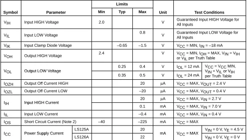
DC CHARACTERISTICS OVER OPERATING TEMPERATURE RANGE (unless otherwise specified)
Limits
Symbol Parameter Min Typ Max Unit Test Conditions
VIH Input HIGH Voltage 2.0 V Guaranteed Input HIGH Voltage for
All Inputs
VIL Input LOW Voltage 0.8 V Guaranteed Input LOW Voltage for
All Inputs
VIK Input Clamp Diode Voltage –0.65 –1.5 V VCC = MIN, IIN = –18 mA
VOH Output HIGH Voltage 2.4 V VCC = MIN, IOH = MAX, VIN = VIH
or VIL per Truth Table
VOL Output LOW Voltage
0.25 0.4 V IOL = 12 mA VCC = VCC MIN,
VIN VIL or VIH VOL Output LOW Voltage
0.35 0.5 V IOL = 24 mA VIN = VIL or VIHper Truth Table
IOZH Output Off Current HIGH 20 µA VCC = MAX, VOUT = 2.4 V
IOZL Output Off Current LOW –20 µA VCC = MAX, VOUT = 0.4 V
IIH Input HIGH Current
20 µA VCC = MAX, VIN = 2.7 V
IIH Input HIGH Current
0.1 mA VCC = MAX, VIN = 7.0 V
IIL Input LOW Current –0.4 mA VCC = MAX, VIN = 0.4 V
IOS Short Circuit Current (Note 2) –40 –225 mA VCC = MAX
ICC Power Supply Current LS125A 20 mA VCC = MAX VIN = 0 V, VE = 4.5 V
ICC Power Supply Current
LS126A 22
mA VCC = MAX
VIN = 0 V, VE = 0 V 2. Not more than one output should be shorted at a time, nor for more than 1 second.
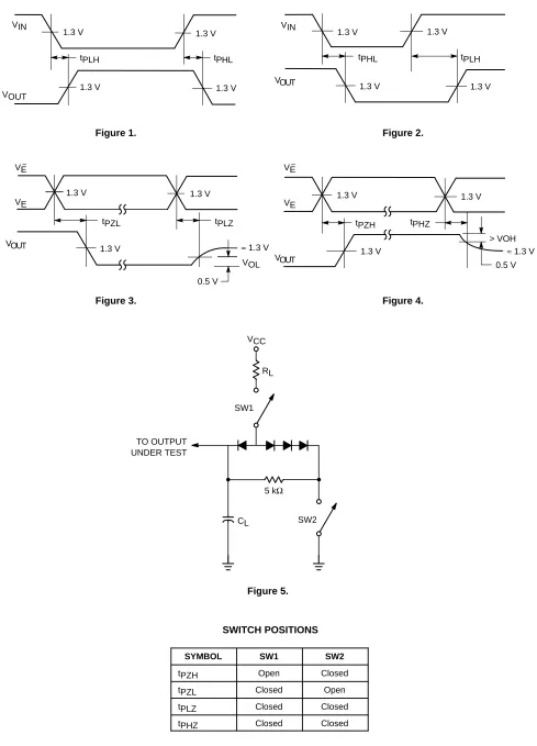
AC CHARACTERISTICS (TA = 25°C)
Limits
Symbol Parameter Min Typ Max Unit Test Conditions
tPLH LS125A 9.0 15
tPLH Propagation Delay, LS126A 9.0 15
ns Figure 2
tPHL
Pro agation Delay,
Data to Output LS125A 7.0 18 ns Figure 2
tPHL LS126A 8.0 18 VCC = 5.0 V
CL 45 pF tPZH Output Enable Time
LS125A 12 20
ns Figures 4 5
CL = 45 pF RL = 667 Ω tPZH Out ut Enable Timeto HIGH Level
LS126A 16 25 ns Figures 4, 5
RL = 667 Ω
tPZL Output Enable Time
LS125A 15 25
ns Figures 3 5 tPZL Out ut Enable Timeto LOW Level
LS126A 21 35 ns Figures 3, 5
tPHZ Output Disable Time
LS125A 20
ns Figures 4 5 tPHZ Out ut Disable Timefrom HIGH Level
LS126A 25 ns Figures 4, 5 VCC = 5.0 V
CL 5 0 pF tPLZ Output Disable Time
LS125A 20
ns FIgures 3 5
CL = 5.0 pF RL = 667 Ω tPLZ Out ut Disable Timefrom LOW Level
LS126A 25
[image:2.612.59.552.69.348.2]Figure 1. Figure 2.
Figure 3. Figure 4.
VIN
VOUT
1.3 V 1.3 V
tPLH tPHL
1.3 V 1.3 V
VIN
VOUT
1.3 V
1.3 V tPHL
1.3 V
tPLH
1.3 V
VE
VE
VOUT
1.3 V
tPZL
1.3 V
tPLZ
1.3 V ≈ 1.3 V
VOL
0.5 V
VE
VOUT
1.3 V
tPZH
1.3 V
1.3 V
tPHZ
> VOH ≈ 1.3 V 0.5 V VE
Figure 5. VCC
RL
SW1
TO OUTPUT UNDER TEST
CL 5 kΩ
PACKAGE DIMENSIONS
1 7
14 8
B
A
DIM MININCHESMAX MILLIMETERSMIN MAX A 0.715 0.770 18.16 18.80
B 0.240 0.260 6.10 6.60
C 0.145 0.185 3.69 4.69
D 0.015 0.021 0.38 0.53
F 0.040 0.070 1.02 1.78
G 0.100 BSC 2.54 BSC
H 0.052 0.095 1.32 2.41
J 0.008 0.015 0.20 0.38
K 0.115 0.135 2.92 3.43
L
M --- 10 --- 10
N 0.015 0.039 0.38 1.01 NOTES:
1. DIMENSIONING AND TOLERANCING PER ANSI Y14.5M, 1982.
2. CONTROLLING DIMENSION: INCH. 3. DIMENSION L TO CENTER OF LEADS WHEN
FORMED PARALLEL.
4. DIMENSION B DOES NOT INCLUDE MOLD FLASH. 5. ROUNDED CORNERS OPTIONAL.
F
H G D
K C
SEATING PLANE
N
–T–
14 PL
M 0.13 (0.005)
L
M
J 0.290 0.310 7.37 7.87
N SUFFIX
PLASTIC PACKAGE CASE 646–06
PACKAGE DIMENSIONS
NOTES:
1. DIMENSIONING AND TOLERANCING PER ANSI Y14.5M, 1982.
2. CONTROLLING DIMENSION: MILLIMETER. 3. DIMENSIONS A AND B DO NOT INCLUDE
MOLD PROTRUSION.
4. MAXIMUM MOLD PROTRUSION 0.15 (0.006) PER SIDE.
5. DIMENSION D DOES NOT INCLUDE DAMBAR PROTRUSION. ALLOWABLE DAMBAR PROTRUSION SHALL BE 0.127 (0.005) TOTAL IN EXCESS OF THE D DIMENSION AT MAXIMUM MATERIAL CONDITION. –A–
–B–
G
P7 PL
14 8
7
1 0.25 (0.010)M B M
S B M
0.25 (0.010) T A S
–T–
F RX 45
SEATING
PLANE D14 PL K
C
J M
DIM MILLIMETERSMIN MAX MININCHESMAX A 8.55 8.75 0.337 0.344
B 3.80 4.00 0.150 0.157
C 1.35 1.75 0.054 0.068
D 0.35 0.49 0.014 0.019
F 0.40 1.25 0.016 0.049
G 1.27 BSC 0.050 BSC
J 0.19 0.25 0.008 0.009
K 0.10 0.25 0.004 0.009
M 0 7 0 7
P 5.80 6.20 0.228 0.244
R 0.25 0.50 0.010 0.019
D SUFFIX
PLASTIC SOIC PACKAGE CASE 751A–03
PACKAGE DIMENSIONS
HE
A1
DIM MIN MAX MININCHESMAX
--- 2.05 --- 0.081
MILLIMETERS
0.05 0.20 0.002 0.008 0.35 0.50 0.014 0.020 0.18 0.27 0.007 0.011 9.90 10.50 0.390 0.413 5.10 5.45 0.201 0.215 1.27 BSC 0.050 BSC 7.40 8.20 0.291 0.323 0.50 0.85 0.020 0.033 1.10 1.50 0.043 0.059
0
0.70 0.90 0.028 0.035 --- 1.42 --- 0.056
A1
HE Q1 LE
10 0 10
LE
Q1
NOTES:
1. DIMENSIONING AND TOLERANCING PER ANSI Y14.5M, 1982.
2. CONTROLLING DIMENSION: MILLIMETER. 3. DIMENSIONS D AND E DO NOT INCLUDE MOLD
FLASH OR PROTRUSIONS AND ARE MEASURED AT THE PARTING LINE. MOLD FLASH OR PROTRUSIONS SHALL NOT EXCEED 0.15 (0.006) PER SIDE.
4. TERMINAL NUMBERS ARE SHOWN FOR REFERENCE ONLY.
5. THE LEAD WIDTH DIMENSION (b) DOES NOT INCLUDE DAMBAR PROTRUSION. ALLOWABLE DAMBAR PROTRUSION SHALL BE 0.08 (0.003) TOTAL IN EXCESS OF THE LEAD WIDTH DIMENSION AT MAXIMUM MATERIAL CONDITION. DAMBAR CANNOT BE LOCATED ON THE LOWER RADIUS OR THE FOOT. MINIMUM SPACE BETWEEN PROTRUSIONS AND ADJACENT LEAD TO BE 0.46 ( 0.018).
ON Semiconductor and are trademarks of Semiconductor Components Industries, LLC (SCILLC). SCILLC reserves the right to make changes
without further notice to any products herein. SCILLC makes no warranty, representation or guarantee regarding the suitability of its products for any particular purpose, nor does SCILLC assume any liability arising out of the application or use of any product or circuit, and specifically disclaims any and all liability, including without limitation special, consequential or incidental damages. “Typical” parameters which may be provided in SCILLC data sheets and/or specifications can and do vary in different applications and actual performance may vary over time. All operating parameters, including “Typicals” must be validated for each customer application by customer’s technical experts. SCILLC does not convey any license under its patent rights nor the rights of others. SCILLC products are not designed, intended, or authorized for use as components in systems intended for surgical implant into the body, or other applications intended to support or sustain life, or for any other application in which the failure of the SCILLC product could create a situation where personal injury or death may occur. Should Buyer purchase or use SCILLC products for any such unintended or unauthorized application, Buyer shall indemnify and hold SCILLC and its officers, employees, subsidiaries, affiliates, and distributors harmless against all claims, costs, damages, and expenses, and reasonable attorney fees arising out of, directly or indirectly, any claim of personal injury or death associated with such unintended or unauthorized use, even if such claim alleges that SCILLC was negligent regarding the design or manufacture of the part. SCILLC is an Equal Opportunity/Affirmative Action Employer.
PUBLICATION ORDERING INFORMATION
JAPAN: ON Semiconductor, Japan Customer Focus Center
4–32–1 Nishi–Gotanda, Shinagawa–ku, Tokyo, Japan 141–0031
Phone: 81–3–5740–2700 Email: [email protected]
ON Semiconductor Website: http://onsemi.com Literature Fulfillment:
Literature Distribution Center for ON Semiconductor P.O. Box 5163, Denver, Colorado 80217 USA
![Clinical evaluation of [123I]FP-CIT SPECT scans on the novel brain-dedicated InSPira HD SPECT system: a head-to-head comparison](data:image/gif;base64,R0lGODlhAQABAIAAAP///wAAACH5BAEAAAAALAAAAAABAAEAAAICRAEAOw==)