ff
Thesis by
Ana Maii Brown
In Partial Fulfillment of the Requirements for the degree of
Doctor of Philosophy
CALIFORNIA INSTITUTE OF TECHNOLOGY Pasadena, California
2016
©2016 Ana Maii Brown
ORCID: 0000-0003-3008-2310
ACKNOWLEDGEMENTS
First and foremost, and with much gratitude, I thank my adviser, Professor Harry Atwater, for his kind guidance and never-tiring enthusiasm and support. I certainly would not have made it through earning a PhD without his encouragement and unwavering confidence in me. I would also like to thank all of the Atwater Group members and staff, and especially Matt Sheldon and Ravishankar Sundararaman for their patient mentorship, and Jennifer Blankenship, Tiffany Kimoto, Daniel Turner-Evans, and Carissa Eisler for their genuine friendship. I am thankful for the blessing of having David Ayala in my life. David has made me a better person, and makes life, with all its mundane and epic moments, more vivid and exquisite. Finally, it is with deep gratitude that I thank my parents, Norm and Adelina, and my sis-ter, Robin, for their unconditional love and steadfast support. Adelina’s inherent strength and humble wisdom, Norm’s unending curiosity and love, and Robin’s ingenuity and devotion to family have shaped me, and yet still leave me in awe.
I am grateful for the generous financial support for my studies and for the work in this thesis, mainly provided by the National Science Foundation and the Link Energy Foundation.
Ana Maii Brown
ABSTRACT
The field of plasmonics exploits the unique optical properties of metallic nanostruc-tures to concentrate and manipulate light at subwavelength length scales. Metal-lic nanostructures get their unique properties from their ability to support surface plasmons– coherent wave-like oscillations of the free electrons at the interface be-tween a conductive and dielectric medium. Recent advancements in the ability to fabricate metallic nanostructures with subwavelength length scales have created new possibilities in technology and research in a broad range of applications.
In the first part of this thesis, we present two investigations of the relationship between the charge state and optical state of plasmonic metal nanoparticles. Us-ing experimental bias-dependent extinction measurements, we derive a potential-dependent dielectric function for Au nanoparticles that accounts for changes in the physical properties due to an applied bias that contribute to the optical extinction. We also present theory and experiment for the reverse effect– the manipulation of the carrier density of Au nanoparticles via controlled optical excitation. This plas-moelectric effect takes advantage of the strong resonant properties of plasmonic materials and the relationship between charge state and optical properties to eluci-date a new avenue for conversion of optical power to electrical potential.
PUBLISHED CONTENT AND CONTRIBUTIONS
Portions of this thesis have been drawn from the following publications:
1. Sheldon, M. T., Van de Groep, J., Brown, A. M., Polman, A. & Atwater, H. A. Plasmoelectric potentials in metal nanostructures. Science346, 828– 831 (2014).
doi:10.1126/science.1258405.
2. Brown, A. M., Sheldon, M. T. & Atwater, H. A. Electrochemical Tuning of the Dielectric Function of Au Nanoparticles. ACS Photonics2, 459–464 (2015).
doi:10.1021/ph500358q.
3. Brown, A. M., Sundararaman, R., Narang, P., Goddard III, W. A. & Atwater, H. A. Non-Radiative Plasmon Decay and Hot Carrier Dynamics: Effects of Phonons, Surfaces and Geometry.ACS Nano10,957–966 (2015).
doi:10.1021/acsnano.5b06199.
4. Brown, A. M., Sundararaman, R., Narang, P., Goddard III, W. A. & Atwater, H. A. Ab initio phonon coupling and optical response of hot electrons in plasmonic metals.Physical Review B(2016). Submitted.
TABLE OF CONTENTS
Acknowledgements . . . iii
Abstract . . . iv
Published Content and Contributions . . . v
Table of Contents . . . vi
List of Illustrations . . . viii
List of Tables . . . x
Chapter I: Introduction . . . 1
1.1 Properties and Applications of Plasmonic Metallic Nanoparticles . . 1
1.2 The Drude and Lorentz-Drude Models . . . 3
1.3 Mie Theory: Scattering of Light by Nanospheres . . . 4
1.4 Beyond the Lorentz-Drude Todel and Mie Theory . . . 5
1.5 Scope of This Thesis . . . 5
Chapter II: The Plasmoelectric Effect . . . 8
2.1 Charge Dependent Dielectric Function . . . 8
2.2 Thermodynamic Model . . . 10
2.3 Temperature Calculations . . . 14
2.4 Calculation of Steady-State Nanoparticle Surface Potential and Charge 17 2.5 Charge Accumulation Shell Model . . . 18
2.6 Nanoparticle Emissivity . . . 19
2.7 FDTD Simulation Methods . . . 20
2.8 Plasmoelectric Simulations . . . 21
2.9 Kelvin Probe Force Microscopy Experiments . . . 23
2.10 Optical Measurements of Nanoparticles Under Monochromatic Illu-mination . . . 28
2.11 Conclusions . . . 32
Chapter III: Electrical Tuning of the Dielectric Function and Optical Proper-ties of Nanoparticles . . . 33
3.1 Previous Work and Overview . . . 33
3.2 Electrochemical Cell Fabrication . . . 34
3.3 Optical Measurements of Nanoparticles Under Applied Bias . . . 36
3.4 Modeling Optoelectronic Effects with FDTD Simulations . . . 40
3.5 Comparison of Simulation and Experimental Results . . . 43
3.6 Conclusions . . . 47
Chapter IV: Completeab initioDescription of Non-Radiative Plasmon Decay 49 4.1 Motivation and Previous Work . . . 49
4.2 Experimental Decay Rate . . . 51
4.3 Electronic Structure . . . 52
4.4 Plasmon Decay via Direct Transitions . . . 53
4.6 Phonon Modes and Matrix Elements . . . 56
4.7 Surface-assisted Transitions . . . 57
4.8 Estimate of Resistive Losses . . . 58
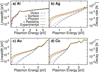
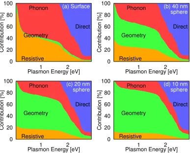
4.9 Results for Common Plasmonic Metals . . . 60
4.10 Conclusions . . . 65
Chapter V: Ab initio Description of Hot Electron Relaxation in Plasmonic Metals . . . 66
5.1 Motivation and Previous Work . . . 66
5.2 Computational Methods . . . 69
5.3 Electronic Density of States and Heat Capacity . . . 69
5.4 Phononic Density of States and Heat Capacity . . . 72
5.5 Electron-phonon Matrix Element and Coupling . . . 74
5.6 Temperature Dependent Dielectric function . . . 79
5.7 Conclusions . . . 87
Chapter VI: Experimental andab initioUltrafast Carrier Relaxation in Plas-monic Nanoparticles . . . 89
6.1 Motivation and Background . . . 89
6.2 Ab initiotheory . . . 93
6.3 Experimental Methods . . . 99
6.4 Results . . . 99
6.5 Conclusions . . . 104
Chapter VII: Summary and Outlook . . . 106
Bibliography . . . 109
Appendix A: Derivations of Expressions for Direct and Phonon-Assisted Plasmon Decay . . . 121
A.1 Direct Transitions . . . 121
A.2 Phonon-Assisted Transitions . . . 123
A.3 Final Expressions for Direct and Phonon-assisted Plasmon Decay After Accounting For Reverse Transitions . . . 129
Appendix B: Tabulated Electronic Heat Capacity and Electron-Phonon Cou-pling Factor as a Function of Electron Temperature . . . 131
LIST OF ILLUSTRATIONS
Number Page
1.1 Sketch of surface plasmon . . . 2
2.1 Absorption cross section spectrum of a Ag nanoparticle and the plas-moelectric effect . . . 9
2.2 Plasmoelectricly Induced Electron Density . . . 10
2.3 Plasmoelectricly Induced Temperature Increase . . . 15
2.4 Au nano particle heat diffusion and temperature . . . 17
2.5 Electron Transfer . . . 18
2.6 Plasmoelectric Potential and Absorption . . . 20
2.7 Nanoparticle Emissivity . . . 21
2.8 Modeled plasmoelectric response for Ag nanoparticles . . . 22
2.9 KPFM Surface Potential Map . . . 24
2.10 KPFM Control Measurement . . . 25
2.11 Plasmoelectric effect on dense Au nanoparticles on ITO/glass . . . . 26
2.12 Schematic of white vs. monochromatic illumination experimental setup . . . 29
2.13 Plasmoelectric effect for 60 nm Au colloids suspended in water . . . 30
3.1 Electrochemical Cell Geometery . . . 35
3.2 Extinction spectra and changes in spectra of Au colloids in electro-chemical cell . . . 37
3.3 Experimental and simulated peak parameters as a function of applied bias . . . 38
3.4 Raw Spectra . . . 39
3.5 FDTD simulation geometry . . . 39
3.6 Physical parameters as a function of applied bias . . . 44
3.7 Comparison of experiment and simulation over full wavelength range 47 4.1 Schematic of Plasmon Decay . . . 50
4.2 Comparison of linewidths . . . 61
4.3 Comparison of contribution to Im(ε) . . . 63
4.4 Carrier Distribution . . . 64
5.1 Fundamental parameters for describing hot electron relaxation . . . . 68
5.3 Electronic heat capacity as a function of electron temperature . . . . 71
5.4 Phonon density of states . . . 73
5.5 Lattice heat capacity as a function of lattice temperature . . . 74
5.6 energy resolved electron-phonon coupling strength . . . 77
5.7 Electron-phonon coupling factorGas a function of electron temper-ature . . . 78
5.8 Ab initiodielectric function at room temperature . . . 82
5.9 Complex dielectric function forTe =400K . . . 83
5.10 Change in dielectric function forTe =300 K to 400 K . . . 83
5.11 Complex dielectric function forTe =1000K . . . 84
5.12 Change in dielectric function forTe =300 K to 1000 K . . . 84
5.13 Complex dielectric function forTe =5000K . . . 85
5.14 Change in dielectric function forTe =300 K to 5000 K . . . 85
5.15 Critical interband transitions for dielectric function temperature de-pendence . . . 87
6.1 Ultrafast transient absorption setup . . . 89
6.2 Differential extinction map as a function of probe wavelength and delay time . . . 91
6.3 Transient differential extinction spectral and kinetic traces . . . 92
6.4 Extinction of Au colloids used in transient absorption measurements . 92 6.5 Electron distribution relaxation evolution . . . 94
6.6 Kinetic signal amplitude dependence on pump power . . . 101
6.7 Transient signal temporal behavior dependence on pump power . . . 101
6.8 Nonthermalized and thermalized electron distribution dependence on pump power . . . 102
6.9 Transient extinction signal for a variety of probe wavelengths . . . . 104
LIST OF TABLES
Number Page
3.1 Simulation parameter limits and resolution . . . 42 4.1 ab initioparameters for metals . . . 60 5.1 Parameters for dielectric function temperature dependence . . . 81 B.1 Tabulated electronic heat capacity and electron-phonon coupling
C h a p t e r 1
INTRODUCTION
1.1 Properties and Applications of Plasmonic Metallic Nanoparticles
The field of plasmonics exploits the unique optical properties of metallic nanos-tructures to route and manipulate light at subwavelength length scales. Recent ad-vancements in the ability to fabricate metallic nanostructures with subwavelength length scales have created new possibilities in technology and research focused on the manipulation of light. Plasmonic metallic nanostructures have been used most successfully to achieve extreme concentration of light, as in plasmonic antennas, lenses and resonators.[1]
Traditionally, light concentration has been achieved with dielectric lenses and res-onators but these devices have limitations that are far surpassed by plasmonic-based metallic nanostructures. The smallest spot size that can be produced with dielectric lenses and resonators is approximately λ/2. Therefore the electromagnetic mode volume in which an optical signal can be concentrated is approximately equal to (λ/2)3; metallic nanostructures can be used to concentrate light to volumes much smaller than these traditional limits.
Metallic nanostructures get their unique properties from their ability to support sur-face plasmons– coherent wave-like oscillations of the free electrons at the intersur-face between a conductive and a dielectric medium (Figure 1.1). Surface plasmons are produced when a time-varying electric field constituting incident light produces a force on the free electrons inside the metal which drives them into a collective oscil-lation in resonance with the incident electric field. Surface plasmons are transverse magnetic in character, and the generation of surface charge requires an electric field normal to the surface. This leads to the field component normal to surface be-ing enhanced near the surface and decaybe-ing exponentially with distance away from it. This field component is evanescent and prevents power from propagating away from the surface. The decay length of the field in the dielectric interfacing with the metal is roughly half of the wavelength of the incident light, whereas the decay length inside the metal is determined by the skin depth.
or-Figure 1.1: Schematic of surface plasmon showing electric fields and oscillating charges. Figure adapted from Reference 2.
der of the exciting optical wavelength; the other form, termed a surface plasmon polariton, is a non-resonant charge-oscillation wave which propagates down the surface of a conductor. Surface plasmon polaritons occur in metal structures with one or more dimensions greater than or equal to the wavelength of incident light; the charge oscillation can propagate down the conducting surface as a surface plas-mon polariton mode. Local surface plasplas-mons occur in metallic nanostructures with dimensions significantly shorter than the dimensions of the incident light, where the whole particle is subject to virtually a uniform incident electric field at any one point in time. This results in dipolar charge separation and resonant frequencies, much like the resonances of a standing wave, which produce a very strong charge displacement and associated field concentration.
because the resonant absorption cross section for plasmonic nanostructures is much larger than their physical cross sections.[16] Recently, there has been considerable interest in plasmonic energy relaxation and conversion mechanisms. Plasmons have relatively short (<10 fs) lifetimes and can decay into single particle excitations, no-tably hot electron-hole pairs.[17] Plasmonic resonators have been recently reported to emit optically excited hot electrons across a rectifying metal-semiconductor in-terface.[18, 19]
Despite more than a decade of intensive scientific exploration, new plasmonic phe-nomena continue to be discovered, including quantum interference of plasmons, observation of quantum coupling of plasmons to single particle excitations, and quantum confinement of plasmons in single-nanometer scale plasmonic particles. Also, plasmonic structures find widening applications in integrated nanophoton-ics, biosensing, photovoltaic devices, single photon transistors, and single molecule spectroscopy.
1.2 The Drude and Lorentz-Drude Models
In 1900 Paul Drude proposed a model of electrical conduction to explain the trans-port and optical properties of electrons in metals.[20, 21] His model approximated a conductor as a collection of free electrons and stationary positively charged ions. In this model, equation of motion for an electron subject to an external electric field
~ Eis
md
2~r
dt2 =−mγ
d~r
dt −eE~(~r,t) (1.1) whereeis electron charge,mis electron mass,r is the electron displacement from equilibrium, and γ is the harmonic damping constant. By considering the con-ductivity of this system and the relation = 1+4πiσ/ω, we arrive at the Drude dielectric function:
(ω)= 1− 4πne
2/m
(ω2+iγω) =1−
ω2
p
(ω2+iγω) (1.2)
wherenis the electron density and the plasma frequency is defined asωp≡ p4πne2/m.
In 1905, Hendrick Antoon Lorentz extended the Drude model to account for elec-trons which are bound by a damped harmonic oscillator to an atom or ion in the solid.[22, 23] The equation of motion for an electron in this Lorentz-Drude model in the presence of an external electric field E is given by the Drude-Lorentz equa-tion:
md
2~r
dt2 = −mω 2
0~r −mγ
d~r
dt −eE(~~ r,t) (1.3) whereω0is the natural frequency of the oscillator, and the other parameters are the
same as those in the Drude model. The dielectric function for this system is given by
(ω)= 1+ 4πne
2/m
(ω02−ω2−iγω) =1+
ω2
p
(ω20−ω2−iγω) (1.4)
The Lorentz-Drude model has been used in investigations to approximate the in-terband contributions to the dielectric function. An extension of the Lorentz-Drude model to more than one oscillator has been used to better approximate the dielectric functions of Ag and Au.[24]
1.3 Mie Theory: Scattering of Light by Nanospheres
Mie theory, which describes the absorption and scattering profiles of a subwave-length sphere illuminated by a plane wave, is named after Gustav Mie, who was the first to electrodynamically describe localized surface plasmon polaritons in metal-lic nanoparticles in 1908.[25] Using Maxwell’s equations, Bohren and Huffman[26] derive the classical analytical solution for the scattering and extinction cross section of the sphere:
Csca =
2π k2
∞ X
n=1
(2n+1)(|an|2+|bn|2) (1.5)
Cext =
2π k2
∞ X
n=1
(2n+1)Re(an+bn) (1.6)
with the scattering coefficients
an=
µm2jn(mx)[xhn(x)]0−µ1jn(x)[mx jn(mx)]0 µm2j
n(mx)[xhn(1)(x)]0− µ1hn(1)(x)[mx jn(mx)]0
(1.7)
bn=
µ1jn(mx)[x jn(x)]0− µjn(x)[mx jn(mx)]0 µ1jn(mx)[xhn(1)(x)]0− µh(1)n (x)[mx jn(mx)]0
(1.8)
where jn and hn are the spherical Bessel functions, x is the size parameter x =
k a, mis the relative refractive index m = k1/k, k and k1 are the wave-vectors in
the particle and surrounding medium, and µand µ1 are the permeabilities of the
1.4 Beyond the Lorentz-Drude Todel and Mie Theory
Mie theory was first experimentally verified in the 1970’s, and as advances in tech-nology have made fabrication and characterization of nanoparticles a common re-search area in recent decades, Mie theory along with the Lorentz-Drude model has been commonly used to describe the optical properties of metallic nanoparticles in a variety of systems. However there are many shortcomings of the Lorentz-Drude model and Mie theory which make them unable to predict or describe nonidealities in real systems, experiments with more complex systems, or microscopic processes related to localized surface plasmons. For example, surfaces and interfaces can change electronic structure and damping, and these effects become more important as the size of nanoparticles decreases.[27, 28] Static or dynamic charge transfer such as those in a system with an applied bias or difference in work function be-tween the plasmonic resonator the the surrounding medium results in a change in the dielectric function and thus to the optical properties.[29, 30] Excitation by in-cident light leads to an increase in temperature of the electron and phonon bath, resulting in changes in the dielectric function as well as in the heat capacity and electron-phonon coupling.[17, 31, 32] When we examine plasmonic behavior at very short time scales, quantum effects become important.[33–35] Without correc-tions for these and other effects, Mie theory with the Lorentz-Drude dielectric func-tion will not accurately predict experimental results. [27, 28] The projects included in this thesis go beyond Mie theory and the Lorentz-Drude Model to achieve more accurate descriptions of plasmonic phenomenon in real systems.
1.5 Scope of This Thesis
Though a variety of projects are presented in this thesis, each study was aimed at furthering the understanding of physical phenomena fundamentally related to plasmons. The chapters are organized as follows:
The Plasmoelectric Effect
with the incident light and reach a thermodynamically favorable state. We provide experimental evidence for the plasmoelectric effect in arrays of gold nanoparticles on an indium tin oxide substrate, where we observed plasmo-electric surface potentials as large as 100 millivolts under monochromatic il-lumination of 100 milliwatts per square centimeter. A spectroscopic analysis of Au nanoparticles in solution showed further evidence for the plasmoelec-tric effect. Plasmoelectric devices may enable the development of all-metal optoelectronic devices that can convert light into electrical energy.
Electrical Tuning of the Dielectric Function and Optical Properties of Nanoparticles
In Chapter 3 we discuss the tunable dielectric response of plasmonic Au nanoparticles under electrochemical bias. We show that the changes in the optical properties of the Au nanoparticles as a function of applied bias can be interpreted in terms of changes in the surface charge density, surface damp-ing, and the near-surface volume fraction of the nanoparticles that experience a modified dielectric function, as well as changes in the index of refraction of the surrounding electrolyte medium. Using experimental bias-dependent extinction measurements, we derive a potential-dependent dielectric function for Au nanoparticles that accounts for changes in the physical properties con-tributing to optical extinction.
Completeab initioDescription of Non-Radiative Plasmon Decay
Chapter 4 describes first-principles calculations that capture all of the signif-icant microscopic mechanisms underlying surface plasmon decay and pre-dict the initial excited carrier distributions so generated. We present the first ab initiopredictions of phonon-assisted optical excitations in metals, which are critical to bridging the frequency range between resistive losses at low frequencies and direct interband transitions at high frequencies. In the com-monly used plasmonic materials, gold, silver, copper, and aluminum, we find that resistive losses compete with phonon-assisted carrier generation below the interband threshold, but hot carrier generation via direct transitions dom-inates above threshold.
and semi-empirical estimates, especially in noble metals above transient elec-tron temperatures of 2000 K, because of the previously neglected selec-trong de-pendence of electron-phonon matrix elements on electron energy. We also present first-principles calculations of the electron temperature dependent di-electric response of hot electrons in plasmonic metals, including direct inter-band and phonon-assisted intrainter-band transitions, facilitating completeab ini-tiopredictions of the time-resolved optical probe signatures in ultrafast laser experiments.
Experimental and ab initio Ultrafast Carrier Relaxation in Plasmonic Nanoparticles
C h a p t e r 2
THE PLASMOELECTRIC EFFECT
It is well known that the plasmon resonance frequency,ωp, of metallic plasmonic
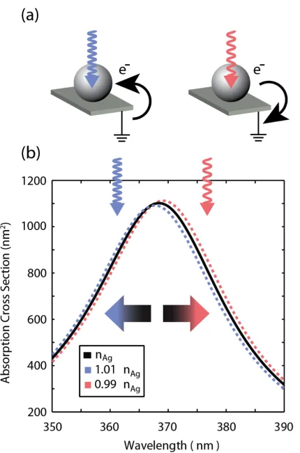
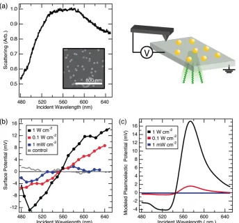
materials is dependent on the electron density. Recent work has demonstrated con-trol overωp of metal nanostructures when an external electrostatic field alters the carrier density in the metal [29]. Increasing the carrier density in a noble metal nanoparticle results in a blueshift of the resonance, whereas decreasing it results in a redshift, as illustrated for a 20-nm-diameter Ag nanoparticle in vacuum in Figure 2.1. But until recently, the reverse effect, the generation of an electrostatic potential due to an optically driven change in carrier density in a plasmonic nanostructure, had not been observed. Thermodynamically, however, such a effect, coined the plasmoelectric effect, is expected to occur. This chapter first discusses the thermo-dynamic model which predicts the plasmoelectric effect, and then presents direct experimental evidence of plasmoelectric potentials in the range 10 to 100 mV on colloidal assemblies, in qualitative agreement with a thermodynamic model. These results may provide a new route to convert optical energy into electrical power.
2.1 Charge Dependent Dielectric Function
Figure 2.1: (a) Schematic: Spontaneous charge transfer to or from the nanoparticle is thermodynamically favored when the consequent spectral shift increases the ab-sorption, raising the temperature. Irradiation on the blue side of the resonance leads to a negative charge on the particle; irradiation on the red side leads to a positive charge. (b) Calculated absorption cross section for a 20-nm-diameter Ag nanopar-ticle in vacuum with bulk carrier densitynAgand carrier densities that are reduced or increased by 1%.
ωp=
ne2
om∗e !1/2
(2.1)
whereeis the electron charge,ois the permittivity of free space, andm∗eis the
elec-tron effective mass [30]. This strategy is consistent with other work that examined carrier density-dependent plasmon shifts, for example in doped semiconductors, electrochemical cells, or at metal surfaces during ultrafast pump-probe measure-ments [10, 37–39].
func-Figure 2.2: Relative change of the absorption cross section, Cabs(n, λ), of a
20-nm-diameter Ag nanoparticle in vacuum, as a function of wavelength and electron density, and normalized by the absorption cross section for a neutral Ag silver par-ticle with electron densitynAg.
tion of wavelength and electron density, and normalized by the absorption cross section for a neutral Ag silver particle with electron density nAg [26]. Note that to the blue of the plasmon resonance increasing electron density increases the ab-sorption cross section, and to the red of the plasmon resonance increasing electron density decreases the absorption cross section.
2.2 Thermodynamic Model Free Energy Minimization
density is achieved when the free energy is at a minimum:
∂F(N,T)
∂N =
∂F
∂N
!
T
+ ∂∂F T(N)
!
N
dT
dN =0 (2.2)
Here, we assume that both the intensity and wavelength of the illumination are constant. Using, by definition, the electrochemical potential µ(N,T) ≡ (∂∂FN)T,
where µ, and the entropy of the particle S(N,T) ≡ −(∂∂FT)N, we find that the free
energy minimum corresponds to a configuration with a number of electrons, N, such that
µ(N,T) = S(N,T)dT(N)
dN (2.3)
Equation (2.3) shows that under illumination, the plasmonic particle adopts an elec-trochemical potential that is proportional todT/dN. This quantity, which is deter-mined only by the plasmon resonance spectrum and the heat flow from the particle to the substrate, provides the unique thermodynamic driving force in the system. It favors charge transfer to or from the particle that increases absorption, and thereby temperature, in order to lower the free energy. The factordT/dN is largest on the steepest parts of the resonance spectrum; it is positive for irradiation on the blue side of the resonance, leading to a positive chemical potential for the electrons and hence a negative voltage. The reverse is observed for irradiation on the red side of the resonance.
Equation (2.2) can be used to quantitatively estimate the equilibrium plasmoelec-tric potential by writing F(N,T) as the sum of the free energies of electrons and phonons, using the well-known free energy functions of an electron and phonon gas [40, 41]. The electronic term is composed of a contribution due to the chemical potential of the electrons that is directly given by the Fermi function, and an elec-trostatic contribution due to charging of the metal nanosphere; the phonon term is given by the Debye model. Taking the derivatives with respect to N andT, we find analytical expressions for µ(N,T) and S(N,T) (see section 2.2) that are then input into Eq. (2.3).
nanoparticle must be equal in steady state. This temperature is a function of the absorption cross section, Cabs, of the nanostructure, which also depends on the
electron density, n, due to the strong dependence on n in the complex dielectric function of the metal. Then, T(n, λ) is the unique thermodynamic state function that distinguishes an illuminated plasmonic absorber from one in the dark.
We assert that it is reasonable to define such a temperature for a resonantly heated particle, because electronic relaxation processes are fast (∼10-100’s fs), after which the electronic system and lattice are in equilibrium. We note that similar arguments are central to, for example, the detailed balance calculation of the limiting efficiency of a photovoltaic cell [42]. This well-defined temperature describes a local thermal equilibrium in a thermodynamic system enclosing the particle, and motivates a ther-modynamic equilibrium argument based on free energy minimization.
Calculation for the Configuration of Minimum Total Free Energy
We determine the total free energy, Ftot, of the nanoparticle by considering the
separate contributions from the electrons,Fe, and the phonons,Fp:
Ftot(N,T(N)) = Fe(N,T(N))+Fp(T(N)) (2.4)
Note that for the optical power densities and time scales we consider, because of the fast electronic relaxation rate and electron-phonon coupling rate in a metal, the electron temperature and phonon temperature are equivalent [17]:
Telectr on≈Tphonon =T(N) (2.5)
Feis defined in terms of the chemical potential of the electrons, µe, and the
electro-static potential on the particle,φ, as
Fe(N,T(N)) =
Z N
0
µe(N0,T(N0))dN0+
Z N−No
0
φ(N0− No)dN0 (2.6)
where No is the number unbound electrons on the neutral particle, and µe is the
Fermi function with a small (< 0.1%) temperature correction [40]
µe(N,V,T(N, λ))= F(N,V)*
,
1− 1
3
πkbT(N, λ)
2F(N,V) !2
+
with
F(N,V) = ~
2m
3π2N V
!2/3
(2.8)
andφis the electrostatic potential for a conducting sphere:
φ(N− No) =
e2(N− No)
4πR0m
(2.9)
where R is the sphere radius, eis the electron charge, and 0 and m are the
per-mittivity of free space and the relative perper-mittivity of the surrounding medium, respectively.
Fpis defined in terms of the speed of sound in the particle,vs, via the Debye
tem-perature,θ, with [41, 43]
Fp(T(N))= 3kbT(N)A0ln
θ
T(N)
!
−kbT(N)A0 (2.10)
and
θ = ~vs
kb
6π2A0
V
!1/3
(2.11)
where kb is Boltzmann’s constant, and A0 the number of atoms in the particle
which here is equal to No. For Au, θ ∼ 170K [40]. Expression (2.11) is the
high-temperature limit of the quantum Debye model, valid forT > θ.
The total electrochemical potential µ and the entropy S can now be derived by applying µ ≡ (∂∂FN)T and S ≡ −(∂∂FT)N to expression (2.4) for the free energy. We
find
µ(N,T(N))= F(N,V)−
mkb2T(N)2
6~2
πV 3N
!2/3
+ e2(N −N0)
4πR0m
(2.12)
and
S(N,T(N))=
Z N
0
1 3
π2k
b2T(N0)
2F(N0)
dN0−3kbA0ln
θ
T(N)
!
+4kbA0 (2.13)
0= F(N)−F(N0)−
mkb2T(N)2
6~2
πV 3N
!2/3
+ e2(N −N0)
4πR0m
−
Z N
0
1 3
π2k2
bT(N 0)
2F(N0)
dN0dT(N) dN
+3kbA0ln
θ
T(N)
!
dT(N)
dN −4kbA0
dT(N)
dN (2.14)
This equation can be solved to find the steady-state value for N (for a given λand Iλ) using as input the function dT(N)/dN, which is determined by the plasmon resonance spectrum and the heat conducted or radiated away from the particle.
Theoretical Efficiency Limit
This thermodynamics model shows that an excited plasmonic resonator behaves as a heat engine that can convert absorbed off-resonant optical power into a static electrochemical potential. In principle, optical-to-electrical energy conversion by this mechanism could be optimized to perform with an efficiency at the Carnot limit, as with any generalized heat engine [44].
2.3 Temperature Calculations Ag Nanoparticle in Vacuum
To calculate the plasmoelectric potential for a Ag nanoparticle in vacuum we cal-culate the temperature of the nanoparticle, T, given the absorption cross section Cabs(n, λ) from section 2.1 and incident power density. Under steady state
illumi-nation, the power absorbed by the particle must equal the power emitted:
Pin = Pout (2.15)
Pin constitutes the absorbed monochromatic optical radiation plus the absorbed
thermal radiation from the ambient background (atTamb= 293K).
Pin =Cabs(n, λ)Iλ +σATamb4 (2.16)
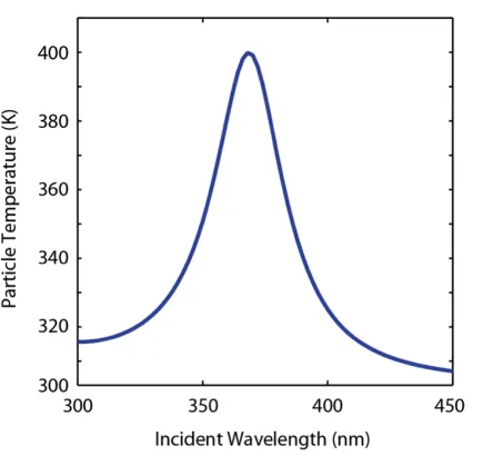
Figure 2.3: Calculated temperature for a 20-nm-diameter Ag particle in vacuum as a function of illumination wavelength (Iλ =1 mW/cm2).
measurement (see section 2.6). This value is close to that of bulk gold and silver in the infrared, as reported elsewhere [45] and that predicted by Mie theory. For a Ag nanoparticle in vacuum the only loss channel for the power is thermal radiation, and thus
Pout =σAT4 (2.17)
Solving Equation (2.15) for the temperature of the particle then gives
T(n, λ) = *
,
Cabs(n, λ)Iλ +σATamb4
σA +
-1/4
(2.18)
Figure 2.3 shows the calculated temperature for a 20-nm-diameter Ag nanoparticle in vacuum as a function of illumination wavelength for an incident power density of 1 mW/cm2; it peaks at 400 K. The calculated temperature and its dependence on N, dT(N)/dN (for a given λandIλ) are then used as input in solving Eqn. (2.14)
for the case of a Ag nanoparticle in vacuum (see section 2.4).
Au Nanoparticle on ITO
To calculate the temperature of a Au nanoparticle on ITO/glass we first calculate the absorption cross section spectrum Cabs(n, λ) using finite-difference-time-domain
in this chapter, the exact dielectric surrounding of the nanoparticle is very complex; there are large variations in inter-particle spacing as well as clusters with different configurations, both inducing near-field coupling and thereby red-shifted resonance wavelengths. Furthermore, Kelvin Probe Force Microscopy (KPFM) experiments were performed in ambient conditions, such that adsorption of water to the particle-ITO interface is likely. Since the exact influence of such conditions on the plas-moelectric potential is beyond the scope of this work, we simplified the geometry to a single 60-nm-diameter Au nanoparticle on an ITO substrate. We assumed a uniform background index of n =1.4 to take into account the red-shift due to the dielectric surrounding described above, such that the modeled scattering spectrum represented the measured scattering spectrum. We then calculated the steady-state power balance to obtain the nanoparticle temperature. Heat flow into the substrate was modeled using a 1D heat transfer model, as sketched in Figure 2.4, with the particle on a glass substrate with thickness d = 1 mm covered by a thin layer of ITO. We used the thermal heat conductivity for glass, σT = 1.05 Wm-1K -1 [46]. The heat of the particle can be transferred from the particle (at Tpart) through a
cylinder of glass with cross sectional area equal to the contact areaAcontactbetween
the glass and the particle, to the bottom of the substrate (at ambient temperature, Tamb= 293 K). The heat flow is given by [46]
Pdi f f = σT
(Tpart−Tamb)
d Acontact (2.19)
Figure 2.4 shows the calculated temperature of the Au nanoparticle as a function of incident wavelength for the three different intensities used in Figure 2.11b. In these calculations the parameter Acontactwas tuned such that the calculations of the
Figure 2.4: (Left) Sketch of 1D heat diffusion model for a Au nanoparticle on ITO/glass. (Right) Au nanoparticle temperature as a function of illumination wave-length, corresponding to the experiments in Figure 2.11b.
compared with a neutral particle is only of order of up to tens of mili-Kelvin, with some variation depending on geometry and illumination intensity. The calculated temperature and its dependence onN,dT(N)/dN (for a givenλandIλ) were used as input in solving Equation (2.14) for the case of Au nanoparticles on ITO/glass (see section 2.4).
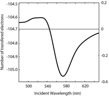
2.4 Calculation of Steady-State Nanoparticle Surface Potential and Charge Using the temperature and values fordT(N)/dN described in section 2.3 we solved Equation (2.14) to determine the steady-state surface potential and corresponding charge on the nanoparticle as a function of irradiation wavelength. Figure 2.5 shows the calculated charge density change (N − No) for Au nanoparticles on ITO/glass,
for the highest experimental power density of Figure 2.4b (Iλ=1000 mW/cm2). The
calculations use 6.67×10⁶Au atoms for a 20-nm-diameter Au sphere. As can be seen, the excess electron number (N−No) is modulated around a value of−104.69
electrons, observed at the peak of the resonance (where there is no plasmoelectric effect,dN/dT = 0). This corresponds to the number of electrons for which the total electrostatic charging energy equals the Fermi energy for Au,EF =5.02 eV. In the
Figure 2.5: Calculated excess electron number N − N0 (right-hand scale) for a
60-nm-diameter Au particle on ITO/glass as a function of illumination wavelength (Iλ
=1000 mW/cm2). The average number of electrons generating the plasmoelectric effect is shown by the right- hand scale.
energy of the ITO substrate, such that the offset observed in Figure 2.5 is in fact the difference in Fermi energy between the particle and the ITO. Correcting for this “dark” charge (right-hand scale in Figure 2.5), we see that in the time-averaged situ-ation less than one electron on average is added or removed from the nanoparticle to generate the observed plasmoelectric potential. The data in Figure 2.5 can be con-verted to surface potential, as shown in Figure 2.11c. Additionally, we note that the thermoelectric effect (omitted in our analysis) induces only a minor contribution to the potential state of the particle, even for large temperature gradients between the substrate and particle, because of the small Seebeck coefficient of metals,∼ µV/∆K [47].
2.5 Charge Accumulation Shell Model
Addition-ally, the plasmon resonance frequency is predominately determined by the electron density of the portion of the particle within the optical skin depth of the metal, as reported experimentally [27] and verified by us using FDTD simulations. There-fore, electrostatic arguments suggest that any additional charges will reside near the surface of the nanoparticle, and electrodynamic arguments suggest that only the electron density near the surface needs to be increased in order to blue-shift the plasmon resonance. If excess charge resides only near the surface, the plasmoelec-tric effect thus requires a smaller number of electrons to obtain the same frequency shift, and therebydT(N)/dN in Equation (2.3) is larger.
To study the influence of non-uniform distributions of charge density in the parti-cle, we consider a simplified shell model, in which we assume that all the additional charge carriers transferred due to the plasmoelectric effect reside in the outer shell with thicknessδ(see inset of Figure 2.6). To implement this shell model in Equation (2.14), one has to express the Fermi energy, temperature, and N andV in terms of the number of electrons in the shell volume rather than in the whole particle. Equa-tion (2.14) can then be solved for the number of electrons in the shell, assuming a certain shell thickness.
Figure 2.6 shows the plasmoelectric potential (a) and the relative increase in absorp-tion (b) for a 20-nm-diameter Ag particle in vacuum, as a funcabsorp-tion of illuminaabsorp-tion wavelength, withIλ =10 mW/cm2, and for different shell thicknesses. Figures 2.6
(a) and (b) clearly show the effect of a thinner shell: the transferred electrons in-duce a relatively larger increase in electron density and thereby a larger increase in absorption. Note that for shell thicknesses larger than 1 nm, the magnitude of the potential rapidly converges to that obtained with uniform charge distribution (δ =10 nm, green curves). Uniform charge distribution is assumed for calculations throughout this chapter. Further arguments for assuming a uniform distribution of charge include the fact that the area under the absorption spectrum of a dipolar plas-mon mode should only scale with the total number of valence electrons in the metal, irrespective of their location inside the particle.
2.6 Nanoparticle Emissivity
emis-Figure 2.6: Calculated induced potential (a) and relative increase in absorption com-pared with a neutral particle (b) for a 20-nm-diameter Ag nanoparticle in vacuum as a function of illumination wavelength for shell thicknesses of 1.0, 2.5, 5.0 and 10 nm (black, red, blue and green trace respectively). The illumination power density is 10 mW/cm2.
sivity of the gold colloids is comparable with bulk gold in the IR, as has been reported elsewhere [45]. Figure 2.7 examines the effect of emissivity on the pre-dicted increase in extinction due to the plasmoelectric effect under monochromatic illumination versus white light illumination (see section 2.10). We find that the dif-ference between the extinction increase forε=1 (which represents a perfect black body) andε = 0.01 (similar to bulk gold) is about one order of magnitude. In the simulations shown in this chapter, we use our experimentally determined emissivity of 0.01.
2.7 FDTD Simulation Methods
We performed full wave modeling using Lumerical finite-difference time-domain (FDTD) [49] simulations to determine the scattering and absorption spectra for Au particles on ITO. Optical constants for Au were, as described in section 2.1, taken from Johnson and Christy [50], and we used the Brendel and Bohrmann model [17] for calculation of the dielectric function. For ITO, optical constants were taken from spectroscopic ellipsometry measurements of sputtered ITO films.
Figure 2.7: Simulated extinction increase compared with white light illumina-tion when Au 60-nm-diameter particles in water are illuminated with 20 mW/cm2 monochromatic illumination for emissivity values,ε, ranging from 1 (perfect black body) to 0.01 (∼bulk gold).
and used to calculate the absorption and extinction spectra.
2.8 Plasmoelectric Simulations
Before applying the model to an experimental geometry (e.g. see Figure 2.11), we first calculated the plasmoelectric potential (i.e., the electrochemical potential gained by the particle from the electron transfer induced by optical absorption) for a spherical 20-nm-diameter Ag nanoparticle in vacuum under monochromatic il-lumination. For these particles, analytical Mie theory can be used to calculate the absorption cross section spectrum, Cabs(λ,n), for a given electron density in the
nanoparticle by taking into account the dependence of the bulk plasma frequency,
Figure 2.8: A 20-nm-diameter Ag particle in vacuum is illuminated with monochro-matic light (Iλ = 1 mW/cm2). (a) Plasmoelectric potential and (b) relative absorp-tion increase as a funcabsorp-tion of incident wavelength.
the intrinsic nonresonant interband absorption in the metal. Figure 2.8b shows the corresponding relative absorption increase for the Ag nanoparticle, which ranges up to a factor of 2.5×10⁻⁵.
The model for the simple geometry in Figure 2.8 describes the key factors in the plasmoelectric effect: an increase in carrier density under illumination at wave-lengths shorter than the resonance peak, inducing a negative plasmoelectric poten-tial and enhanced absorption relative to the neutral particle. Similarly, radiation at longer wavelengths induces a lower carrier density, a positive plasmoelectric poten-tial, and enhanced absorption. These results demonstrate that an excited plasmonic resonator behaves as a heat engine that can convert absorbed off-resonant optical power into a static electrochemical potential.
a background index of n= 1.4 for the medium above the ITO substrate, such that the absorption spectrum matched the experimentally observed spectrum. As can be seen in Figure 2.11c for the high-power data, the modeled trends correspond well with the experimental trends: the modeled minimum potential occurs at 530 nm (experimental: 500 nm), the modeled zero potential occurs at 545 nm (experimen-tal: 560 nm), and a large positive potential is observed for wavelengths above the resonance, both in model and experiment. The extent of the measured potential to wavelengths up to 640 nm in Figure 2.11b is in agreement with the long-wavelength tail in the spectrum of Figure 2.11a. At 555 nm, the modeled particle temperature peaks at 308 K, 15 K above ambient, in good agreement with other experimental observations [45].
2.9 Kelvin Probe Force Microscopy Experiments
To experimentally probe the plasmoelectric potential, we measured the surface elec-trostatic potential of films of 60-nm-diameter Au colloid nanoparticles deposited on ITO under optical excitation while varying the wavelength of monochromatic illu-mination as shown in Figure 2.11. Kelvin probe force microscopy (KPFM) was used to characterize the surface potential. Briefly, a conductive atomic force mi-croscope (AFM) tip employed in non-contact mode determined the static potential difference between the tip and sample surface, indicating the work function dif-ference as well as any trapped charges or other induced potentials at that location. This technique allowed us to measure plasmoelectric potentials induced on the Au particle surfaces as a function of illumination wavelength.
Colloid Desposition
Figure 2.9: KPFM surface potential map of three 60-nm-diameter Au nanoparticles shows the work function offset of Au vs. ITO while the sample was in the dark.
deposited on the surface. Subsequently, the substrates were rinsed thoroughly with DI water and heated to 290 C by placing a heat gun 5 cm above the sample sur-face for 20 minutes. The scattering spectra of the deposited samples (as in Figure 2.11a) were obtained using a Zeiss Axio Observer inverted microscope equipped with a 20× dark-field objective, with illumination from a halogen lamp. Figure 2.11a shows the measured scattering spectrum for a sample, showing a clear plas-mon resonance aroundλ =550 nm.
KPFM Measurement Methods
To probe the local static potential difference between the tip and sample surface at room temperature, we used an Asylum Research MFP-3D AFM in scanning Kelvin probe microscopy mode with a n+silicon conductive tip (Nanosensor ATEC-EFM-20) to measure the surface potential of the ITO-coated glass substrate samples, with the ITO film connected to ground [51]. Figure 2.9 shows that the technique gives mV resolution of the work function difference between Au nanoparticles and ITO, detecting the greater surface electron density of Au compared with ITO when the sample was dark.
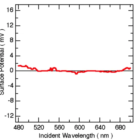
Figure 2.10: KPFM-measured surface potential from a control experiment of bare ITO/glass under 1W/cm2scanned monochromatic illumination, plotted on the same scale as Figure 2.11b.
ITO substrate adjacent to the nanoparticle array was compared with the dark signal.
The sample was measured at the limit of highest available particle coverage, and it was anticipated that the measured region of ITO/glass adjacent to the Au parti-cles was equipotential with the partiparti-cles. Direct illumination of the AFM tip was avoided, and there was no dependence of the magnitude of signal based on the distance from the optical spot, within ∼10’s of µm. A control measurement of ITO/glass free of Au colloids shown in Fig 2.10 shows no detectable wavelength-dependent signal. The absolute surface potential determined by the KPFM tech-nique is a convolution of the work function difference between the sample and the particular tip used, and factors relating to the tip-sample geometry that define ca-pacitance. Therefore, to emphasize wavelength-dependent changes of potential, the reported data (Figure 2.11b) are plotted relative to the surface potential in the same spot measured in the dark before optical excitation.
Measured Plasmoelectric Potentials
tentials during excitation to the blue side of the neutral-particle plasmon resonance wavelength near 550 nm, and positive potentials during excitation on the red side of the resonance, with the measured potential changing sign near the peak of the plasmon resonance. The magnitude of the signal increases with increasing optical power density, except at the neutral particle resonance. These data provide evidence for induced plasmoelectric potentials and are consistent with the modeled plasmo-electric response. Notably, these trends are not consistent with the thermoplasmo-electric effect. The thermoelectric potential would be maximized at the plasmon resonance, due to the maximal induced heat absorption at that frequency. By contrast, we ob-serve no induced potentials at the plasmon resonance frequency. A thermoelectric potential would also not be expected to change sign based on the wavelength of illumination. Further, even a temperature increase in the particles several hundred Kelvin greater than predicted by our model would induce thermoelectric potentials of only a few hundred µV based on the Seebeck coefficient of bulk Au [47]. This small voltage is below the limit of our measurement sensitivity. However, some off -set in the data may be due to the thermoelectric response of the substrate. Control samples of ITO with no Au particles show a weak constant positive potential,∼ 1 mV, during wavelength scans at high optical intensity. Direct illumination of the AFM tip was avoided during measurements.
wavelengths would more significantly decrease positive plasmoelectric potentials. Circuit non-idealities, such as contact resistance between the Au and ITO, may also contribute to a reduction in the plasmoelectric potential. In our studies it was nec-essary to anneal samples for more robust signal, presumably to remove residual surface ligands from the Au colloid, reducing the contact resistance.
2.10 Optical Measurements of Nanoparticles Under Monochromatic Illumi-nation
The plasmoelectic model predicts that when illuminated to either side of the plas-mon resonance with plas-monochromatic radiation, the charge density of a plasplas-monic resonator in contact with a electron reservoir will change such that the absorption cross section will shift towards the illumination wavelength. It follows that the spec-tra of Au colloids measured with scanned monochromatic light will show a broader resonance peak than the resonance peak in a spectra measured with white light. We performed optical extinction spectroscopy for 60-nm-diameter Au colloids in wa-ter to characwa-terize this plasmoelectric response. The changes in the surface charge density of the particles can result from induced polarization across the metal-water interface.
Experimental Setup
To measure the extinction of 60-nm-diameter Au colloids (BBI International, EM.GC60 Batch #15269, OD1.2) in water under broadband (white) and monochromatic illu-mination, we used lock-in amplifiers (LIA) in combination with two photodiode power meters and a monochromator. The measurements setup is shown in Figure 2.12. For broadband illumination, the cuvette with Au colloids was positioned in front of the monochromator (sample position 1). For the monochromatic illumi-nation conditions, the cuvette was placed in between the two photodiodes. The extinction can easily be obtained by comparing the signal on both power meters for each illumination wavelength and normalizing by spectra of a cuvette with DI water placed in the same two positions as the sample.
Measured Spectral Dependence on Illumination Properties
Figure 2.12: Schematic of white vs. monochromatic illumination experimental setup
Modeled Optical Plasmoelectric Response
To model the increase in extinction during monochromatic illumination in a wa-ter environment, we calculate the thermal energy of the system in diffusion-limited conditions (i.e. particles are in thermal equilibrium with the water) that correspond with the experimental procedure. Assuming that the water in the cuvette is a ther-mally isolated system, all the power absorbed by the nanoparticle suspension will heat the water (thermal radiation is negligible), and the system will increase its tem-perature. Using the laser power (∼1 mW max), scan speed (1 nm/s), the extinction (measured, see Figure 2.13a), the fraction of extinction that goes into absorption (known from Mie theory), the heat capacity of water, and the volume of water in the cuvette, we calculate that the temperature increase during monochromatic illu-mination is∼1 mK per second at the highest illumination intensity in our study. We then calculate the thermal energy of a volume of water heated per particle under illumination. Given the particle concentration of the suspension (2.6×10¹⁰mL−1), this corresponds to a maximum ∼ 1.6× 10⁻¹³ J of thermal energy provided per particle. To solve the governing relation Equation (2.7), the change of this ther-mal energy per change of surface charge density on the particle (due to changes of absorption) is equated to the change of electrochemical potential. Full wave simu-lations (FDTD method) were used to calculate the extinction based on the charge density that satisfied Equation (2.7) at each incident wavelength and power, and is depicted in Figure 2.13c.
2.11 Conclusions
To aid interpretation of our findings, we comment briefly on other mechanisms for generating photopotentials in metals. A thermoelectric effect is several orders of magnitude weaker (∼ µV/K) than the observed potentials as discussed above [47]. Hot carrier-induced effects would require rectifying contacts, which are not present in our geometry. Moreover, both of these effects would not result in a bisignated signal [18]. “Plasmon drag” or similar direct photon-to-electron momentum trans-fer mechanisms on Au colloids would not produce a bisignated signal [52]. Future work in this area will benefit from further insight into the microscopic mechanisms that contribute to the observed effect.
C h a p t e r 3
ELECTRICAL TUNING OF THE DIELECTRIC FUNCTION
AND OPTICAL PROPERTIES OF NANOPARTICLES
3.1 Previous Work and Overview
the various contributions that shape plasmonic resonances is crucial for current re-search in tunable plasmonics, and more broadly, for any system in which plasmonic elements will be used an a non-neutral state, e.g. as catalysts or electrical contacts.
Previous experiments have shown that externally biased Au nanoparticles (AuNPs) are not adequately described by the Drude model [17, 26, 27, 60, 64, 68, 71]. A potential-dependent modified dielectric function and T-matrix-based fitting routine has been proposed to analyze interface damping and uniform charging effects for Au nanorods in an electrochemical cell [68]. This work provided a systematic model for bias-dependent extinction, but did not explicitly address index changes in the surrounding media or non-uniform distribution of charge at the particle surface [68, 72]. Separately, the effects of various surface layers on the dielectric response of Au nanoparticles in an electrochemical cell were investigated, in comparison with modeling that relied on analytical Mie Theory, though analysis of broadening ef-fects and the role of the refractive index of the substrate were not considered [24, 27, 72]. These researchers found evidence of increased damping at a positive ap-plied bias, which they attributed to a lossy layer at the particle surface. Previous research has not analyzed the effects of changes in the surrounding dielectric en-vironment, changes in damping, and concentration of excess charge at the particle surface all occurring in unison. In this Chapter, we present mechanisms for bias-dependent optical extinction of Au nanoparticles, using full wave electromagnetic simulations in conjunction with experimental optical spectra to characterize the re-sponse of arrays of colloidal Au nanoparticles immobilized on indium tin oxide (ITO) substrates in an electrochemical cell. Through this combined simulation and experimental approach, we account for the influence of refractive index due to the substrate, index changes in the near-surface environment of the nanoparticle, and a variable-thickness shell of modified damping and charge density at the surface of the gold nanoparticle (AuNP). We compare the simulations with experimental results to quantitatively analyze the contributions from these effects.
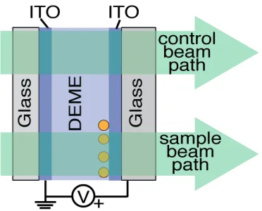
3.2 Electrochemical Cell Fabrication
Figure 3.1: Geometry of electrochemical cell with 60-nm-diameter AuNPs on the bottom electrode. The top electrode is grounded, and potentials are applied to the bottom electrode. An optical beam passes through the cell for spectral measure-ments
half of the bottom electrode for use as a control in the normalization of optical spectra; this allowed us to carefully control for a possible optical response from the ITO substrate as a function of applied bias. The bottom electrode was placed in a glass scintillation vial (ITO-side up) with 300 µL of 60-nm-diameter Au col-loids in water (BBI International, EM.GC60 Batch #16516 OD1.2) and 1.5 mL of deionized (DI) water. 60 µL 0.1 M HCl was added to the vial, and the vial was immediately centrifuged at 2000 rpm (∼670 g-force) for 40 minutes. After centrifuging, the Au colloid solution had become clear and the bottom ITO elec-trode has a noticeable red color due to Au nanoparticles deposited on the surface. The Parafilm wax was removed from the bottom electrode and the electrode was rinsed thoroughly with DI water then soaked in toluene for one hour to remove residue from the Parafilm wax. Both electrodes were plasma etched with a di-rect plasma at 110 W and 300 mTorr O2 for 20 minutes to remove ligands and
3.3 Optical Measurements of Nanoparticles Under Applied Bias Experimental Setup and Procedures
In our experiment, the spectra of an ensemble of 60-nm-diameter Au colloids in an electrochemical cell were recorded as a function of applied bias. The applied bias was swept from 0V to 2.25V and then to -2.25V and back to 0V in 0.25V steps. The top electrode was grounded and potentials were applied to the bottom electrode using a DC voltage source (Tektronix PS282).
The extinction spectra of an array of AuNPs in the electrochemical cell were ob-tained using a spectral response and lock-in amplifier technique. The beam from a supercontinuum pulsed laser (20 MHz, Fianium SC400-2) was chopped at 100 Hz and directed into a monochromator (Oriel 777000) that was optically in-series with two Si photodiodes (the first photodiode was used as a reference). The spectral res-olution of the monochromator was approximately 1.5 nm. The photodiode signals were passed through transimpedance amplifiers (DL Instruments 564) and were de-tected by lock-in amplifiers (SR830 DSP). Spectra with the optical beam passing through the portions of the bottom electrode with and without Au colloids were collected at each applied bias step. The spectra taken in the portion of the bottom electrode without Au colloids were used as normalization spectra. Approximately 20 minutes elapsed between each voltage step and the corresponding spectral mea-surement.
Optical Measurement Results
Figure 3.2: (a) Extinction versus wavelength at selected applied potentials as indi-cated by line color. (b) Extinction change versus wavelength at the same applied potentials in (a).
This is in contrast to what we would expect based on the Drude model and Mie the-ory [17, 24, 26], which predict a peak height change that decreases monotonically as a function of increasing electron density. This suggests that, at the very least, there was significant damping in the experimental system at positive potentials that is not captured by a Drude and Mie theory model.
Raw Spectra and Noise Level
Figure 3.4: Normalized raw spectra at the extremes of the applied bias cycle (2.25V and -2.25V) as well as the first 0V point ( 0V Start) and the 0V point in the middle of the applied bias cycle (0V Middle).
3.4 Modeling Optoelectronic Effects with FDTD Simulations
Three-dimensional full wave electromagnetic simulations were performed using fi-nite difference time domain methods to model and analyze the experimental system. The simulation geometry consisted of a 60-nm-diameter Au nanosphere on an ITO substrate and in a surrounding medium with uniform index of refraction ( Figure 3.5 ). The ITO substrate was defined by the real and imaginary part of the complex index of refraction, measured with ellipsometry. The AuNP was simulated as a core defined by the Brendel and Bormann (BB) [56, 57, 72, 73] dielectric function with the additional feature of a variable-thickness shell with a modified dielectric func-tion. The BB model uses a superposition of an infinite number of oscillators (termed a BB oscillator) to replace the single Lorentz oscillator used in the Lorentz-Drude model [24, 60, 72, 74]. The BB dielectric function is defined as:
BB(ω)=1−
ω2
p
ω(ω−iΓo)+ k P
j=1
χj(ω)
(3.1a)
ωp=
s
noe2 ome
(3.1b)
whereΓois the damping constant of bulk gold, χj(ω) is a BB oscillator,ωpis the
plasma frequency in the Drude model, no is the electron density of bulk gold, eis
the elementary charge, and me is the effective electron mass. Six BB oscillators
were used in our parameterization. We obtain an analytic function that satisfies the Kramers-Kronig reciprocity relations for real and imaginary components of the dielectric function. This model has been shown to accurately model the optical properties of gold in the wavelength range relevant to this study [24, 28, 75–78].
Voltage-dependent Dielectric Function
A modified dielectric function at the surface of the particle was used to model changes in the electronic states and population near the surface:
shell(ω,s) =1−
ωp,v(s)2
ω(ω−i(Γo+ΓV(s)))+ k P
j=1
χj(ω)
(3.2a)
ωp,V(s) = s
n(s)e2
ome
Here,ωp,V(s) andn(s) are state (s) dependent variables, where the state describes
the applied bias (V) applied to the cell and the microscopic state of the system, and these state-dependent variables have replaced the respective constant values used in the BB model. An additional, state-dependent damping term ΓV(s) was added
to the bulk damping to allow for changes for damping at the particle surface as a function of the state of the system (largely the applied bias).
Parameter Sweeps and FDTD Simulations
The independent parameters that were varied in our analysis are: the index of sur-rounding electrolyte, and ΓV and n(s) in the shell dielectric function, as well as
the thickness of this shell. Additionally, to account for polydispersity in the size of particles (8% coefficient of variation as reported by the supplier), we performed electromagnetic simulations for particles with 28, 30, and 32 nm radii and took a weighted average of the resulting spectra to produce simulated extinction spectra for polydisperse samples for each parameter set (surrounding-index, ΓV, n(s), and
shell-thickness). We performed calculations where each of these parameters was varied independently. For each unique parameter set, a full-wave electromagnetic simulation was performed with Lumerical FDTD Solutions software to simulate the extinction spectra corresponding to that parameter set. This approach allowed us to calculate a set of predicted extinction spectra from the effect of changes in index, interface damping changes, and surface charging occurring in parallel. We began with broad parameter sweeps where the values for parameters found in cur-rent literature describing damping, surface effects, charging, or electric double layer were well within the sweep limits [24, 27, 28, 71, 75]. The limits for the parameter sweeps are shown in Table 3.1.
champion set of parameters for each applied bias step. The champion parameters values for these simulations then represented the identifiable physical properties and changes in the system as determined by our model. These parameters are those shown in Figure 3.6.
Physical Interpretation of Simulation Parameters
We believe the model described above represents the most comprehensive analysis to date of the microscopic mechanisms that can contribute to bias-dependent opti-cal extinction for metal nanoparticles. We now discuss the physiopti-cal basis for the observed variation of nanoparticle parameters. Because gold oxide has a larger di-electric constant than the electrolyte solution, oxidation of the AuNP surface will cause changes of the index of refraction at the surface of the metal nanoparticle relative to an unoxidized Au particle [28, 56, 57, 73, 79]. Further, the refractive index of the surrounding medium could also change due to alignment of dipoles in the electrolyte, as in an electric double layer [60, 64, 67, 70, 71, 74]. Damping may also be modified by an applied bias because of variations of population or depop-ulation of electronic surface states at the AuNP surface [28, 75–78]. For example, an applied bias could facilitate enhanced chemical reactivity and adsorption at the particle surface and electrons may become trapped in empty adsorbate states, caus-ing an increase in dampcaus-ing[28, 79]. Alternatively, an increase in electron density due to a negative applied bias could result in electron spill-out from the surface and repulsion of solvent molecules from the AuNP surface [53, 80, 81]. This could con-ceivably give rise to a decreased damping due to a decrease in chemical reactivity and trap state occupation at the particle surface. It is also reasonable to assume that the applied bias will alter the total number of electrons in the AuNP and thereby alter the plasma frequency in accordance with the Drude model [29, 65]. In the electrostatic limit, mobile charges will rearrange to minimize the electric fields in the bulk of a conducting particle, so we assume that excess electrons or holes reside near the particle surface. Finally, the modified electronic states and electron density
Table 3.1: Simulation parameter limits and resolution
Parameter Lower Limit Upper Limit Finest Resolution
Surrounding Index 1.0 1.7 0.001
Shell Charge (n/nAu %) 0.95 1.05 0.005
Shell Thickness (nm) 0 5 0.25
at the surface may have a variable penetration depth that depends on the applied bias because of the aforementioned electron spill-out, adsorbate states, and the op-tical versus the static skin depth of excess charge residing near the surface. We account for changes in the penetration depth of altered electronic states by varying the thickness of the modified dielectric shell in our simulations.
3.5 Comparison of Simulation and Experimental Results
By varying the charging, damping, shell thickness, and electrolyte index indepen-dently of one another in our parametric calculations and by computing their net influence on the extinction spectra, we were able to closely model the experimental changes in the extinction as a function of applied bias with full wave electromag-netic simulations. Figure 3.3 shows a comparison of the spectral properties of the simulated and experimental spectra. We see that the best-fit simulations closely track the peak position, height and changes in width. Furthermore, in Figure 3.3d, we show the experimental and best-fit simulated spectra at the extrema of the ap-plied bias range (2.25V and -2.25V) as well as at the first 0V apap-plied bias point, with very good agreement between the curves. We note that the absolute FWHM is sensitive to peak broadening due to particle size polydisparity and other ensemble effects[29, 71] that are not well captured by our FDTD simulations, though changes of FWHM (Figure 3.3c) are primarily due to changes in damping, and therefore are expected to be tracked well by our analysis method. From Figure 3.6a we note that the maximum RMSE of the fits of the simulated and experimental spectra was less than 0.8% of the experimental 0V peak extinction.
bias becomes more positive, the electron density decreases, and then increases as the applied bias becomes more negative, as expected; however, there is significant hysteresis which is not consistent with reversible, ideal charging. The overall shell charge density range for the applied potentials used was within 3% of the neutral charge density. The hysteresis upon charging/discharging is strongest in the first half of the applied bias cycle (from 0 V to 2.25V and back to 0V). This is a common feature in cyclic voltammetry measurements and may be due to initial chemical reactions or “settling” of the system during this initial application of an electric field.
The results for the damping parameter exhibit an overall trend of increased damping at positive biases and decreased damping at negative biases ( Figure 3.6c ). The damping coefficient used in the BB model to best describe neutral, bulk Au metal isΓo =7.596×10¹³rad/sec [67]. At the first 0V data point, we found the damping
constant was 1×10¹³ rad/sec less than this value, indicating that the damping of plasmons on the AuNPs in this system is less than in bulk gold. Recalling that this data point corresponds to a 1% elevation of electron density in the particle shell, we speculate that the decreased damping could be due to electron spill-out and a resulting interlayer where the solvent is repelled and electron trapping in surface or adsorbate states is decreased, resulting in an electron configuration that experiences less damping than in the bulk. At+2.25V, we found ΓV = 3×10¹³ rad/sec. The
increase in damping at positive applied voltages is consistent with prior published work [27, 28, 56, 58], and may be due to excitation of sp-electrons in adsorbate states at the surface of the particle. Again, at negative voltages, as in the first 0V case, we found that the damping was lower than for neutral, bulk Au metal, (at -2.25V, ΓV = −6.6 × 10¹³ rad/sec) and we similarly attribute this to decreased
reactivity and electron spill-out at the particle surface.