International Research Journal of Engineering and Technology
(IRJET)
e-ISSN: 2395-0056 Volume: 06 Issue: 02 | Feb 2019 www.irjet.net p-ISSN: 2395-0072© 2019, IRJET | Impact Factor value: 7.211 | ISO 9001:2008 Certified Journal
| Page 2614
DESIGN OF DUAL FREQUENCY PROBE FED MICROSTRIP ANTENNA
USING SHORTING WALL
Sanjay S.Kulkarni
11
Extc. Dept., Shivajirao S. Jondhle College of Engineering& Technology, Asangaon (Thane), India.
---***---Abstract:- Communication between humans was first bysound through voice. With the desire for slightly more distance communication came, devices such as drums, then, visual methods such as signal flags and smoke signals were used. These optical communication devices, of course, utilized the light portion of the electromagnetic spectrum. It has been only very recent in human history that the electromagnetic spectrum, outside the visible region, has been employed for communication, through the use of radio. One of humankind’s greatest natural resources is the electromagnetic spectrum and the antenna has been instrumental in harnessing this resource.
Dual-frequency operation of antennas has become a necessity for many applications in recent wireless communication systems, such as GPS, GSM services operating at two different frequency bands, and services of PCS and IMT-2000 applications. Although there are various techniques to achieve dual-band operation from various types of microstrip antennas, there is no efficient design tool that has been incorporated with a suitable optimization algorithm. The cavity-model based simulation tool or the design of dual-band microstrip antennas, using multiple slots in the patch or multiple shorting strips between the patch and the ground plane. Since this approach is based on the cavity model, the multiport approach is efficiently employed to analyze the effects of the slots and shorting strips on the input impedance. Then, the optimization of the positions of slots and shorting strips is performed to achieve an acceptable antenna operation over the desired frequency bands. The antennas designed by this efficient design procedure were realized experimentally, and the results are compared. In addition, these results are also compared to the results obtained by the commercial electromagnetic simulation tool, the FEM-based software HFSS by ANSOFT.
Introduction
The rectangular microstrip antenna can be designed for the dual frequency or multi frequency application using shorting wall. The shorting wall is a small copper strip which is connected on the ground plane side and which is inserted upto the rectangular radiating patch by making a slot or cut. The slot is made at the edge depending upon the thickness of the strip or wall (nearly 1mm, thickness considered in project model) the strip is inserted and then soldered. The various effects observed or the results seen are being shown in the later part of this chapter.
Design of antenna:
To design the antenna the general steps of fabrication are followed as given below:
1. Selection of substrate:
The substrate which is the fiber epoxy material is about 1mm thick and has copper clad on both sides, for this project two prototype models made up of Alumina and Kingster were used. The dimension of the clad is 9cm×11cm.
2. Layout and itching:
The rectangular patch of about 5cm×6cm was to be made. The patch was made by the artwork and the required patch was covered or masked. The itching was done by two ways: a) By dipping in ferric chloride solution. b) By exposing to ultraviolet rays. The sample antenna was itched using ferric chloride solution but for better accuracy the unwanted copper was removed by exposing to ultraviolet rays.
3. Making of slot:
To connect the shorting wall a slot of 1mm thick and length of 2cm is done by using a zig-saw machine, similarly a hole of 0.8mm is made for the connection of co-axial probe connector.
4. Soldering:
The shorting wall and probe connector is soldered by suitable soldering material and soldering gun. A care is to be taken that the strip reaches upto the surface of radiating patch and connection is properly done.
Antenna geometry:
Volume: 06 Issue: 02 | Feb 2019 www.irjet.net p-ISSN: 2395-0072
© 2019, IRJET | Impact Factor value: 7.211 | ISO 9001:2008 Certified Journal
| Page 2615
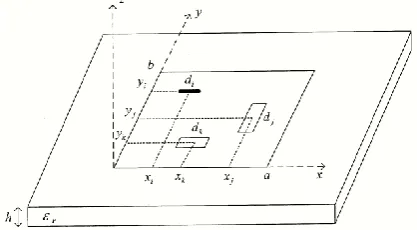
magnetic field has only x and y components in the regionbounded by the microstrip patch and the ground plane,
Figure 1.a. Geometry of a microstrip antenna with one probe feed x -directed and One y-directed shorting pin.
Figure 1.b. Geometry of a microstrip antenna with one probe feed and two slots.
Fig.1 In addition, using the fact that the electric current density on the microstrip patch has no normal component along the edge of the patch, the tangential magnetic field is assumed to be negligible not just at the edges of the patch but all the way down to the ground plane. Therefore, the region between the patch and the ground plane can be surrounded by perfect magnetic conductor (PMC) wall that would not significantly alter the original field distribution under the patch, and hence forms a cavity. Consequently, once the cavity is formed as the model of the patch antenna, the fields in the cavity and subsequently other electrical characteristics can be easily obtained by the well-known solution of the cavity.
[image:2.595.53.268.129.250.2]The design of antenna to obtain dual frequency using a probe fed is as shown in figure 2, figure a. shows the antenna simulation using ANSOFT-HFSS software and figure b. shows its practical design to study the various parameters of antenna.
[image:2.595.56.265.296.411.2]Figure 2.a: Antenna as in HFSS design
Figure 2.b: Antenna model (actual)
The fig 2.a shows an antenna with a co-axial feed point at the left hand (lower bottom of the patch) and a shorting wall connected at the edge parallel to x-axis, and perpendicular to y-axis, indicated by a black line. Figure 2.b shows the actual photograph of an antenna and the size compared with a line tester.
Antenna specifications:
• 1. Electrical specification :
Band width = 5%
Gain= 5.46dBi
Side lobe level = 13dBi
Width length ratio = 80%
Power handled =0 .21watt
Beam width = 500
• 2. Mechanical specification :
Height = 6.54mm
Size 3”x3.4”x3”
International Research Journal of Engineering and Technology
(IRJET)
e-ISSN: 2395-0056 Volume: 06 Issue: 02 | Feb 2019 www.irjet.net p-ISSN: 2395-0072© 2019, IRJET | Impact Factor value: 7.211 | ISO 9001:2008 Certified Journal
| Page 2616
Antenna results:The simulation of antenna is done using ANSOFT-HFSS software and following results are obtained for the various parameters.
1. S–Parameter (Return loss):
S–Parameter
Return loss is a way to express the reflection coefficient in logarithmic terms (dB). The red curved line is the simulated return loss. This is the impedance of the antenna, as the frequency is scanned from 1.5 GHz to 4 GHz. Each point on the line represents the impedance at a particular frequency. Points As the frequency is decreased, the impedance changes. At f = 3.3 GHz, we have the third band on the sharp impedance. At this point, the antenna is resonant, which means the impedance is entirely real. The frequency is scanned down until f=1.75 GHz, producing the locus of points (the red curve) that represents the antenna impedance over the frequency range. At f = 2.4 GHz, the impedance is inductive, and the reflection coefficient is about 0.65, since it is closer to 3 independent resonance.
2. VSWR:
VSWR
The curve demonstrates that, dual band is achievable in simulated and measurement results. For higher frequency band 2:1 ratio is achieved with minimum VSWR 1.2 As shorting ratio decreases from 1 to 0.1, the measured resonance frequency reduces from 1.2 GHz to 3.7 GHz implying nearly 32% reduction. The
maximum error between the theoretical and experimental resonance frequencies is 4.2%. With decrease in shorting ratio from 1 to 0.1, the real part of the measured Zin increases from 50.7 Ω to 52.8Ω. In order to obtain impedance matching with the 50Ω coaxial line, the feed point has to be shifted closer to the edge side.
Results obtained practically:
The figure shows the result obtained on the network analyzer for the antenna design. It is observed that according to the simulated results and the height of the shorting wall, if the height of the wall is increased than the antenna is resonant at higher frequencies and if the height is smaller the antenna is resonant for lower frequencies. It is also seen that the antenna can be used for multi-resonant frequency depending upon the height of shorting wall. The comparison of VSWR and Return loss can be done according to the figures shown below. The appendix 1 & 2 shows the return loss using 15mm & 10mm shorting wall height as well as VSWR for 15mm & 10mm shorting wall.
Appendix-1
Return loss (15mm shorting wall)
Appendix-2
© 2019, IRJET | Impact Factor value: 7.211 | ISO 9001:2008 Certified Journal
| Page 2617
Appendix-3VSWR. (15mm shorting wall)
Appendix-4
VSWR.( 10mm shorting wall)
Conclusion
Dual-frequency operation of rectangular patch antennas with shorting strips and slots has been investigated via the cavity model in conjunction with the multiport theory. An efficient and accurate design tool was proposed for dual-band microstrip antennas using multiple vertical strips or slots. For the examples provided in this study, the frequency ratio of the high-band and low-band frequencies, and the input impedances over these bands were used as the specifications, while the coordinates and dimensions of the strips or slots were the optimization parameters. The antennas so designed have been realized, and dual-band operation was verified experimentally as well as by simulation of the antennas rigorously via HFSS by Ansoft. It is observed that the theoretical results agree well with the experimental results. Therefore, this approach can be safely proposed as an efficient CAD tool for dual-band microstrip antennas that would use slots or vertical strips, at least for the initial design of the antennas.
References
1. J.R. James and P.S. Hall, Hand Book of Micro strips Antenna, Vol. 1, Peter Peregrnus Ltd., 1989.
2. C.A. Balanis, “Antenna Theory Analysis and Design”, 2nd ed; Willey New York, 1997.
3. G. Kumar and K.P. Ray, “Broadband Microstrip Antennas”, Artech House, 2000.
4. Kin-Lu Wong “Compact Broadband Microstrip Antennas”, John Willey & sons. Inc., New York, 2002.
5. HFSS Ansoft software for stimulation of MSA.
6. R. Porath, “Theory of miniaturized shorting-post micro-strip antennas,” IEEE Transactions, Antennas and Propagation, Vol. 48, No. 1, pp. 41-47, 2000.
7. M. Sanad, “Effect of the shorting posts on short circuit microstrip antennas,” Proceedings, IEEE Antennas and Propagation Society International Symposium, pp. 794-797, 1994.
8. R. Garg, P. Bhartia, I. Bahl, and A. Ittipiboon, “Micro-strip antenna design handbook,” Artech House: London, 2001.
9. K. L. Wong and W. S. Chen, “Compact microstrip an-tenna with dual-frequency operation,” Electronics Letters, Vol. 33, No. 8, pp. 646-647, 1997.
10. A. Vallecchi, G. B. Gentili, and M. Calamia, “Dual-band dual polarization microstrip antenna,” Proceedings, IEEE International Symposium, pp. 134-137, 2003.
11. E. Lee, P. S. Hall, and P. Gardner, “Compact dual-band dual-polarization microstrip patch antennas,” Electronics Letters, Vol. 35, pp. 1034-1036, 1999.
12. James, J. R., and P. S. Hall, Handbook of Microstrip Antennas, Vol. 1, London: Peter Peregrinus, Ltd., 1989.
13. Sanad, M., ‘‘Effect of the Shorting Posts on Short Circuit Microstrip Antennas,’’ IEEE AP-S Digest,
1994, pp. 794–797.
14. Satpathy, S., K. P. Ray, and G. Kumar, ‘‘Compact Microstrip Antennas Using a
15. Single Shorting Post,’’ Proc. NSAML, New Delhi, India, March 1998, pp. 69–72.
International Research Journal of Engineering and Technology
(IRJET)
e-ISSN: 2395-0056 Volume: 06 Issue: 02 | Feb 2019 www.irjet.net p-ISSN: 2395-0072© 2019, IRJET | Impact Factor value: 7.211 | ISO 9001:2008 Certified Journal
| Page 2618
17. Bahl, I. J., and P. Bhartia, Microstrip Antennas,Dedham, MA: Artech House, 1980.
18. George, J., et al., ‘‘New Compact Microstrip Antenna,’’ Electronics Letters, Vol. 32, No. 6, 1996, pp. 508–509.