http://wrap.warwick.ac.uk/
Original citation:
Barry, Nicolas P. E., Pitto-Barry, Anaïs, Sanchez, Ana M., Dove, Andrew P., Procter,
Richard J., Soldevila-Barreda, Joan J., Kirby, Nigel, Hands-Portman, Ian, Smith, Corinne
J. I., O’Reilly, Rachel K., Beanland, R. and Sadler, Peter J.. (2014) Fabrication of
crystals from single metal atoms. Nature Communications, Volume 5 . Article number
3851 .
Permanent WRAP url:
http://wrap.warwick.ac.uk/61803
Copyright and reuse:
The Warwick Research Archive Portal (WRAP) makes this work of researchers of the
University of Warwick available open access under the following conditions.
This article is made available under the Creative Commons Attribution- 3.0 Unported
(CC BY 3.0) license and may be reused according to the conditions of the license. For
more details see
http://creativecommons.org/licenses/by/3.0/
A note on versions:
The version presented in WRAP is the published version, or, version of record, and may
be cited as it appears here.
Received 13 Jan 2014|Accepted 10 Apr 2014|Published 27 May 2014
Fabrication of crystals from single metal atoms
Nicolas P. E. Barry
1, Anaı¨s Pitto-Barry
1, Ana M. Sanchez
2, Andrew P. Dove
1, Richard J. Procter
1,
Joan J. Soldevila-Barreda
1, Nigel Kirby
3, Ian Hands-Portman
4, Corinne J. Smith
4, Rachel K. O’Reilly
1,
Richard Beanland
2& Peter J. Sadler
1Metal nanocrystals offer new concepts for the design of nanodevices with a range of potential applications. Currently the formation of metal nanocrystals cannot be controlled at the level of individual atoms. Here we describe a new general method for the fabrication of multi-heteroatom-doped graphitic matrices decorated with very small, ångstro¨m-sized, three-dimensional (3D)-metal crystals of defined size. We irradiate boron-rich precious-metal-encapsulated self-spreading polymer micelles with electrons and produce, in real time, a doped graphitic support on which individual osmium atoms hop and migrate to form 3D-nanocrystals, as small as 15 Å in diameter, within 1 h. Crystal growth can be observed, quantified and controlled in real time. We also synthesize the first examples of mixed ruthenium–osmium 3D-nanocrystals. This technology not only allows the production of ångstro¨m-sized homo- and hetero-crystals, but also provides new experimental insight into the dynamics of nanocrystals and pathways for their assembly from single atoms.
DOI: 10.1038/ncomms4851 OPEN
1Department of Chemistry, University of Warwick, Gibbet Hill Road, Coventry CV4 7AL, UK.2Department of Physics, University of Warwick, Gibbet Hill Road, Coventry CV4 7AL, UK.3Australian Synchrotron, 800 Blackburn Road, Clayton, Victoria 3168, Australia.4School of Life Sciences, University of Warwick, Gibbet Hill Road, Coventry CV4 7AL, UK. Correspondence and requests for materials should be addressed to N.P.E.B.
T
ailoring nanoscopic objects is of importance for the production of the materials of the future, for example in medicine, industrial manufacturing, construction and space exploration1–4. The potential for use of metal nanocrystals has long been recognized. For example, colloidal gold was first made by Andreas Cassius in 1685 (ref. 5), and notably also by Michael Faraday in 1857 (ref. 6). Since then, a range of techniques has allowed the fabrication of nanocrystals, and these have allowed detailed investigation of their size-dependent properties7.The recent emergence of powerful methods such as
high-resolution transmission electron microscopy, has enabled the design and the observation of a variety of nanometer-sized objects, from graphene matrices, to nanoparticles and nanotubes8,9.
The process of crystallization, the formation of microscopic periodic arrangements of atoms, ions and molecules, has long been a topic of intense fascination. It is 100 years since William Henry Bragg and his son William Lawrence Bragg revolutionized the characterization of crystalline solids by showing that the atomic structure of a crystal is related to its X-ray diffraction pattern10. Understanding the dynamics of crystal formation is also of great interest as the mode of assembly can influence the type of periodic lattice which is formed, and hence the properties of the resulting crystals. However, the direct observation of resolved single atoms, atom-by-atom cluster formation and the crystallization process for nanoscopic crystals is still an experimental frontier11–15. Currently, formation of such crystals cannot be controlled at the level of individual atoms16–20, and understanding the metal dynamics of nanocrystal formation relies mostly on computation18–20.
Here we introduce a new general method for the fabrication of multi-heteroatom-doped graphitic matrices decorated with very small, angstrom-sized, three-dimensional (3D)-metal crystals of defined size. This technology allows experimental observation of crystal assembly from single metal atoms and captures the dynamics of metal cluster formation in real space with atomic precision. We irradiate boron-rich precious metal-encapsulated self-spreading polymer micelles with electrons and produce, in real time, a doped graphitic support on which individual metal atoms hop and migrate to form 3D-nanocrystals, as small as 15 Å in diameter and within 1 h. Crystal growth can be observed, quantified and controlled in real time. Our procedure is exemplified by osmium, the densest of all metals21, and gives rise to osmium crystals, which are among the smallest reported22, embedded into a B/S-doped graphitic support. As an example of the generality of the procedure, we also synthesize the first examples of mixed ruthenium–osmium 3D-nanocrystals. This technology not only allows the production of angstrom-sized homo- and hetero-crystals, highly novel materials with potentially
useful and unusual properties, but also provides new
experimental insight into the dynamics of nanocrystals and pathways for their assembly from single atoms.
Results
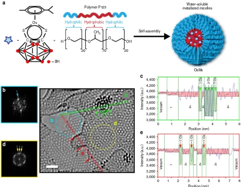
Preparation of precursors. Our procedure involved the encapsulation of the organometallic half-sandwich OsII arene complex [Os(p-cymene)(1,2-dicarba-closo-dodecarborane-1,2-dithiolate)] (1), a 16-electron complex23, which is highly hydrophobic24; in the water-soluble amphiphilic triblock copolymer P123 (ref. 25) at ambient temperature for 4 h to form OsMs micelles (Fig. 1a). The OsMs micelles were fully characterized by a range of techniques, including synchrotron small-angle X-ray scattering (SAXS) experiments (see Methods, Supplementary Figs 1–6, and Supplementary Table 1). These
analyses demonstrated that complex 1 and polymer P123
self-assemble in solution to give core/shell micelles with very low-dispersity parameters (0.161), containing 52±6 P123
unimers, along with 52±11 complex 1. They have a core
diameter of 9.06±0.12 nm, and a shell diameter of
6.50±0.15 nm, giving a total-diameter of 15.56±0.27 nm. The
data are summarized in Supplementary Table 1. OsMsmicelles are dispersible in water. They contain a defined number of metal complexes, and are deformable on surfaces since P123 polymer forms stable Langmuir films at ambient
temperature26. Thus, we deposited aqueous droplets
([OsMs]¼1 mg ml1) onto lacey carbon-coated grids to produce an unsupported film over the grid holes for examination by aberration-corrected high-resolution transmission electron microscopy (HR-TEM).
Formation of a graphitic matrix and Os nanocrystals. We observed structural changes within the Pluronic film upon irradiation with the high-energy electron beam (80 keV; 1.9 pA cm2or 7.6107electronsnm2s1). The emergence of atomic ordering within the self-supporting matrix consistent with a turbostratic graphitic structure was apparent within a few minutes, and a highly structured few-layer graphene lattice was evident after 50 min. An analysis of this matrix is shown in Fig. 1. The existence of individual layers of single-sheet graphene-like material at the edges of the material was demonstrated by fast Fourier transform (FFT) analysis (Fig. 1b), while few-layer graphene-like material was also visible (Fig. 1c shows a region with three layers). Along with these structural modifications of the self-supporting polymeric film, a rapid decomposition of the carborane-containing complex1was also observed (in less than 1 min), and Os atoms could be imaged either singly or as small-ordered clusters (Fig 1c,e), which is currently at the forefront of such experiments9,17,27,28.
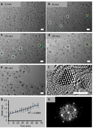
Electron energy loss spectroscopy not only confirmed the identity of the Os atoms, but also suggested that boron and sulfur from the carborane ligand in1are present in the graphitic matrix (Supplementary Fig. 7). Notably, sites with Os clusters (Supplementary Fig. 7c) appear to be close to both high-boron (Supplementary Fig. 7b,e,f) and high-sulfur sites (Supplementary Fig. 7a,d,f). Interestingly, boron and sulfur atoms are also seen throughout the entire matrix suggesting the formation of a multi-heteroatom-doped graphitic matrix. After 1 min of irradiation, clusters ofca.0.7 nm were already visible (Fig. 2a). After 5 min of irradiation, dark areas containing ca. 15 atoms, became more organized and larger (ca. 1.0 nm, Fig. 2b). Further growth of the nanoclusters on the self-supporting matrix was evident after 15 min of irradiation (Fig. 2c), and after 30 min, osmium metal clusters with diameters of ca.1.2–1.6 nm were visible (Fig. 2d).
Growth was observed until ca. 60 min (Fig. 2), and the
nanoclusters were seen to roll on the support in a series of images recorded within a minute (Supplementary Video 1). The movement of energized nanoclusters themselves results in contact with neighbouring particles, and eventual merging. Such cluster merging is illustrated in Supplementary Fig. 8 (also Supplementary Video 2). Interestingly, Zoberbieret al.9reported that clusters of 20–60 Os atoms inside carbon nanotubes continuously change their shape under the influence of an 80 keV electron beam, and bind strongly to the inner surface, weakening C–C bonds and promoting gradual removal of carbon atoms.
Measurements of the length of the clusters indicate a linear relationship with time (Fig. 2g). This description is however only indicative owing to the 3D nature of the nanocrystals (Supplementary Video 3). Significantly, this in situ generation of Os atoms on a self-supporting graphitic matrix produces 3D
nanoclusters that are crystalline29. This is illustrated by the fast Fourier transform (FFT) analysis (Fig. 2h) of the ca. 1.5 nm-diameter Os nanocrystal depicted in Fig. 2f. Supplementary Fig. 9 shows a montage of 10 osmium crystals along with their corresponding FFT analyses. In general, the Os crystals do not seem to have a simple hexagonal structure. Supplementary Fig. 10 shows two particles from the montage in Supplementary Fig. 9 with the closest appearance to the hexagonal structure and compares them with simulations. The c-axis view is distinctive, and the a-axis view is a good fit, with the correct interatomic distances. Nevertheless, we believe that most of the images do not match either of these two views, which are not the only ones with views that look relatively simple. The other views have more complex behaviour dependent on particle size and microscope focus. However, the average Os–Os distance measured over 85 different nanocrystals was determined to be 0.257±0.019 nm,
close to that in crystals of bulk osmium metal (0.27048 nm as the nearest neighbor distance at 293.15 K)30,31. No change in Os–Os distance was observed during nanocrystal growth, as shown by the narrow standard deviation for the average Os–Os distance
calculated from these 85 nanocrystals of various sizes (width between 1.5 and 2 nm).
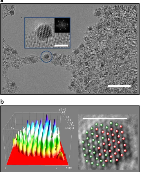
Mixed Os/Ru nanocrystals. To demonstrate the generality of this new technology, we encapsulated 1 mol equivalent of osmium complex 1 and 1 mol equivalent of its ruthenium analogue [Ru(p-cymene)(1,2-dicarba-closo-dodecarborane-1,2-dithiolate)] inRuOsMsmicelles, spread them onto a lacey carbon grid and irradiated them with the electron beam in a similar procedure as described above. Again, it was possible to observe metal atom migration and nanocrystal formation on a timescale of ca. 1 h (Fig. 3).
The composition of the crystals was analyzed by a combination of scanning-TEM and energy-dispersive X-ray analysis at the single particle level (Supplementary Fig. 11); this clearly demonstrated their hetero-metallic Ru/Os nature. Interestingly, the Ru/Os molar ratios determined for 55 different crystals (0.91±0.07/1.13±0.07) are very close to the initial Ru/Os ratio in
theRuOsMsmicelles determined by inductively coupled plasma a
Os
Polymer P123
Hydrophilic Hydrophobic Hydrophilic S
S
C =
= BH
C + H O
20 20
4,400
4,200
4,000
3,800
3,600
Intensity (a.u.) 3,400
3,200 Vacuum
1 2+ 2+
1 Os 2 Os 1 Os
2+
3,000
4,400
4,200
4,000
3,800
3,600
Intensity (a.u.) 3,400
3,200
3,000
0 1 2 3 4
Position (nm)
5 6 7 8
0 1 2 3
Position (nm)
4 5 6
70
O O
Self-assembly
Water-soluble metallated micelles
OH
CH3
b
d
d
c
b
e
c
e
OsMs
Vacuum Vacuum
1 2+ 1 2+ 2+
[image:4.595.56.539.50.425.2]1 Os 1 Os 1 Os
Figure 1 | Micelle formation and analysis after irradiation with electrons.(a) Self-assembly of block copolymer micellesOsMscontaining
mass spectrometry (ICP-MS) (0.83±0.10/1.11±0.13). This suggests that the atomic percentage of each metal in the nanocrystals can be readily tuned by varying the ratio of metal complexes encapsulated in the micelles, opening-up new perspectives for the design of hetero-metal nanocrystals with defined size and composition.
Discussion
We investigated the pattern and the rate of single Os movement by following the positions of a single Os atom over 200 s (20 frames with 10 s between each frame; Supplementary Fig. 12c, Supplementary Fig. 12d). The positions were extracted from the movie shown in Supplementary Video 4. Attempts were made to correlate the ‘hopping’ pattern with three different mechanisms: edge-to-edge, bridge-to-bridge and hole-to-hole hopping over the hexagonal graphitic matrix (Supplementary Fig. 12a,b). The closest fit corresponds to Os atoms moving from bridge-to-bridge
(that is, sitting between a pair of two adjacent atoms) at a rate of 0.0089±0.0016 nm s1. Such a bridge localization of Os atoms is
apparent in some HR-TEM pictures (Supplementary Fig. 13), and is consistent with the favoured location of Pt atoms adsorbed on boron-doped graphene predicted by calculations18. Moreover, extrinsic point and line defects, such as foreign atoms at different positions, strongly modify the charge distribution and the electronic structure of graphene32. Density functional theory calculations have also suggested that graphitic boron dopants induce a deficiency of charge in graphene sheets, while sulfur doping of graphene is of particular interest as the resulting materials are expected to have a wider band gap than pure graphene33. Boron-doped graphene films show a large number of Stone-Wales defects34, while calculations indicate that sulfur doping induces a large local curvature that tends to increase the local reactivity35. Metal atoms have a high affinity for non-perfect and strained regions of point defects in graphene created by electron irradiation and annealing36. Thus, boron and sulfur
2.5 (60 min) (15 min)
a b
c d
e f
g h
(30 min) (5 min) (1 min)
2
1.5
1
0.5
0
0 10 20 30 40 50 60 70 Time (min)
R2 = 0.9486
[image:5.595.142.456.46.479.2]Width (nm)
Figure 2 | Time-dependent formation of Os nanocrystals on the graphitic matrix.(a–d) Migration of small clusters and their coalescence
(for example, clusters in yellow and dark blue circles merge to give crystal in green circle) over a period 1–30 min; scale bars, 2 nm. (e) The abundance of nanocrystals after 60 min. (f) Typical example of an Os crystal of ca. 1.5 nm, formed after 30 min of irradiation, scale bar, 1.5 nm. (g) Width of the clusters/crystals versus time. The error bars are the standard deviations from the mean for measurements of the width of at least 20 clusters at each timepoint. (h) Fast Fourier transform analysis of the nanocrystal shown inf.
centres and the resultant defects might act as centres, which attract Os atoms. This was confirmed by HR-TEM images showing that Os atoms are located in disturbed zones of the hexagonal pattern of the matrix (Supplementary Fig. 14). Individual Os atoms were also observed at step edges (Fig. 1d); similar observations have been reported for Au and Pt atoms on graphene layers37.
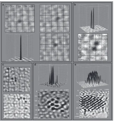
Such atom-by-atom fabrication of di- and poly-atomic molecules led to the rapid assembly of Os atoms into clusters. Figure 4 shows the atom-by-atom formation of osmium molecules, clusters made up of a few Os atoms and nanocrystals. This appears to be the first observation of atom-by-atom fabrication of nanocrystals.
In conclusion, our synthetic technology provides a new route to the in situ generation of an unsupported graphitic matrix together with metal atoms, which can migrate to form crystals. The method not only allows the multi-doping of the graphitic matrix, in this case with both boron and sulfur, but also captures the dynamics of metal cluster formation in real space with atomic precision. Indeed, this first report of the use of block copolymer micelles to encapsulate metal complexes for in situreduction to metal atoms and formation of nanocrystals has allowed the
dynamics of formation of metal nanocrystals to be observed, all the way from single atoms to molecules, clusters and then nanocrystals. This method has been exemplified by the production of a graphitic matrix doped with sulfur and boron, decorated with ångstro¨m-sized crystals of osmium, opening-up possible new perspectives for the design of nanoscopic highly-dense and pressure-resistant materials. The technology can readily be extended to expand the range of dopants in the supporting graphitic matrix, for example by replacing sulfur with selenium. It is also facile to fabricate a range of homo- and hetero-metal angstrom-size nanocrystals. We have illustrated this for mixed ruthenium–osmium crystals. Other combinations that might be readily accessible include Pd, Rh, Ir and Au, as the synthesis of the precursor carborane complexes of these metals is feasible. There is also wide scope for adapting this polymer-encapsulated metal complex synthetic procedure by variation of the block copolymer. The possibility of creating individual vacancies at desired locations in carbon nanotubes using electron beams has been recently demonstrated38, and might also be combined with our procedure to allow the grafting of Os nanocrystals onto specific hotspots. Our synthetic route, which gives rise to a self-supporting graphitic matrix, also offers attractive possibilities for studying the formation of multi-heteroatom-doped-graphitic sheets and the influence of dopants and defects without influence from the underlying support grids (for example, copper), a problem which often complicates the interpretation of metal deposition experiments. A combination of new experiments and computation will be necessary in future work for fully understanding the detailed mechanisms of doping, hopping, cluster rolling and coalescence. Finally, these nanocrystals may contribute to conceptual advances in the design of a new range of nanodevices, for example, for information storage, electronic circuitry, chemosensing and catalysis.
Methods
Materials.The preparation of the complex [Os(p-cym)(1,2-dicarba-closo
-dodecaborane-1,2-dilthiolate)] (1) was based on a previous report23. The triblock copolymer P123 [poly(ethylene glycol)-block-poly(propylene glycol)-block -poly(ethylene glycol)] was purchased from Sigma-Aldrich and used as received. Anhydrous tetrahydrofuran (Aldrich) was used. Pure water (18.2 MO) was collected from a Purelab UHQ USF Elga system. Holey carbon grids with 200 mesh and lacey carbon grids were purchased from Quantifoil Micro Tools Gmbh and Elektron Technology UK Ltd, respectively and used as received.
Synthesis of OsMs and OsRuMs.A tetrahydrofuran solution (1 ml) of complex1
(5 mg ml1) was added to an aqueous solution (10 ml) of polymer P123
(5 mg ml1) and the resultant mixture was stirred at ambient temperature for 4 h. The solution was then dialyzed to remove the tetrahydrofuran (molecular weight cutoff¼1000 Da), for 48 h, and then freeze-dried. A similar procedure was used for synthesizingOsRuMswith 1 mol equivalent of1, 1 mol equivalent of the Ru analogue and 1 mol equivalent of polymer P123.
Characterization of the micelles OsMs and P123Ms.Dynamic light scattering
(DLS) experiments (Supplementary Fig. 2) unambiguously demonstrated that polymer P123 and complex1self-assemble in aqueous solution. Encapsulation decreased the size of P123Ms micelles from 19.6±1.80 nm (hydrodynamic diameter,Dh) to 11.5±2.35 nm forOsMswith aÐof 0.03 (Supplementary Fig. 2a; Supplementary Table 1). Although micellar size usually increases after encapsu-lation of organic molecules39, incorporation of hydrophobic molecules can result in
expulsion of water from the micelles, causing a contraction40. The hydrophobicity
of1probably results in a stronger folding of the poly(ethylene oxide) chains around the complex through hydrophobic interactions, with concomitant expulsion of water from the core. A small second population ofOsMsparticles (o0.01% in number) was found atDhB220 nm, exhibiting a strong intensity in DLS analysis, owing to the aggregation of some particles (Supplementary Fig. 2c).
Cryogenic TEM (cryo-TEM) analysis without staining was then performed on Quantifoil carbon-coated grids to observe the morphology of the hydrophobic core (containing osmium complexes) of the nanoparticles in solution. The high contrast provided by the heavy osmium centres allowed facile imaging of the osmium-polypropylene glycol (PPG) core, but impaired the observation of the poly(ethylene glycol) corona owing to the polymer hydrated state; and disfavored by the small
0
0.4 0.3 1 2
1 2 x (nm)
x (nm) y (nm)
0 0.4 0.8 1.2 1.6 2 2.4
0.2
a
[image:6.595.47.290.56.352.2]b
Figure 3 | Ru-Os 3D-nanocrystals from RuOsMs micelles.(a) An array of
diameter of the micelles (Supplementary Fig. 3a), even after attempts to further stain the samples with uranyl acetate. From these experiments, it was clear that spherical micellar morphologies are formed when polymer P123 encapsulates complex1. The observed diameter of theseOsMsnano-spheres is 7.85±1.97 nm (Supplementary Fig. 3b) with very low close-to-ideal dispersity, based on counting 157 particles counting (1.06, 1.00 being for ideal mono-disperse systems; see Supplementary Table 1). These data are in accordance with theDhdetermined by DLS within experimental error.
To gain further insight into their structures in aqueous solution, and to confirm cryo-TEM and DLS results,OsMsand P123Ms were analyzed by synchrotron SAXS (Supplementary Fig. 4). The experimental profiles were fitted to three model functions for spherical micelles: SphereForm, CoreShellSphere, and
PolyCoreShellRatio (PCR). The PCR model fitted excellently for both micelles with very low-Ðparameters (0.161 forOsMsand 0.146 for P123Ms, 0 being an ideal mono-disperse system, Supplementary Table 1). These analyses demonstrated that OsMsself-assembly leads to core/shell micelles with a core diameter of 9.06±0.12 nm, and a shell diameter of 6.50±0.15 nm (Supplementary Table 1).
The core dimension ofOsMswas larger than that of P123Ms (6.74±0.06 nm),
while the corona dimension ofOsMswas smaller than that of P123Ms shell (12.22±0.17 nm). The diameters ofOsMsmicelles by DLS and cryo-TEM are in
accordance with the core diameter determined by SAXS within the experimental
errors, while the diameters of P123 micelles from DLS and SAXS studies are similar.
From these data (scattering length density calculations, degrees of polymerization of Pluronic P123 and the molecular formulae of the polymer and of complex1; see Instrumentation and Methods), aggregation numbers for OsMsand P123Ms micelles were determined as 20±2 monomer chains per
P123Ms micelle and 52±6 monomer chains perOsMsmicelles. Determinations of osmium by ICP-MS gave a polymer/complex1ratio of 1/1±0.091 for
OsMsshowing that the 52 chains polymer chains self-assembled with 52±11
complexes1(see Supplementary Table 1). Similar core/shell diameters (Supplementary Table 1) with excellent fits to the PCR model were obtained from experiments at three different concentrations (1, 5, 10 mg ml1; Supplementary Fig. 4a,b) for bothOsMsand P123Ms. Hence concentration does not influence the micellar structure, a parameter of importance for Pluronic-type self-assemblies.
Instrumentation
Ultraviolet-visible spectroscopy. Ultraviolet-visible absorption spectra were recorded on a temperature-controlled Varian CARY 300 Biospectrophotometer using 1-cm path-length quartz cuvettes (0.5 ml).
a b
c d e
0.4 0.8 1.2 1.6 2.0 0.4
0.8 1.2 1.6 2.0
y (nm)
y (nm)
0
x (nm)
x (nm)
3.5 2.5 1.5 0.5
3.5 2.5 1.5 0.5
0.6
0.8 0.4 0.2
0 0.2 0.4 0.6
y (nm)
x (nm)
0.6 0.8 0.4 0.2
0 0.2 0.4 0.6
0
y (nm)
[image:7.595.82.517.46.508.2]x (nm)
Figure 4 | Atom-by-atom formation of osmium molecules clusters and eventually crystals.(a) 3D projection showing high contrast for a single
Os atom, together with three 2D projections showing movement of the Os atom at a rate of 0.0177 nm s1over a period of 160 s. (b–c) Formation of dimer, trimer and tetramer molecules. (d) A cluster of eight Os atoms. (e) A ca. 25 Å crystal. All the images show the same region.
Inductively coupled plasma mass spectrometry.Osmium (189Os) content was determined using an ICP-MS Agilent technologies 7500 series instrument. The standard for osmium was purchased from Aldrich. Calibration curves were prepared using Os standard solutions in double deionised water with 3% nitric acid, ranging between 50 and 0.5 ppb (9 points). Samples were freshly prepared in double deionised water with 3% nitric acid. Readings were made in no-gas mode with a detection limit of 1 ppt for189Os.
Dynamic light scattering. The Dh of nanoparticles was determined by DLS. Typically, an aqueous nanoparticle solution was measured with a Malvern Zetasizer NanoS instrument equipped with a 4 mW He-Ne 633 nm laser module at 25°C. Measurements were carried out at a detector angle of 173°(back scattering). Data were analyzed by the Malvern DTS 6.20 software.Dhwas calculated by fitting the apparent diffusion coefficient in the Stokes–Einstein equationDh¼kT/(3pZDapp), wherekis the Boltzmann constant,Tis the temperature andZis the viscosity of the solvent.Dhcoincides with the hydrodynamic diameter when the sample is made of monodispersed spherical particles (Dappequals the translational diffusionDt).
Transmission electron microscopy.TEM was performed using a JEOL 2000FX operating at 200 kV. TEM samples were prepared by using holey and lacey carbon grids. One drop of the sample solution (5ml) was applied to the grid and after 2 min the solution was blotted away before drying. Images were recorded on a Gatan Orius camera and were analyzed using ImageJ software. At least 100 particles from different parts of the grid were counted for each sample to obtain the average diameter.
Cryogenic-transmission electron microscopy.A JEOL 2010F TEM was operated at 200 keV and images were recorded on a Gatan UltraScan 4000 camera for cryo-TEM and glow discharge. The samples were prepared at ambient temperature by placing a droplet on a TEM grid. The extra liquid was then blotted with a filter paper and the grid was inserted in liquid ethane at its freezing point. The frozen samples were subsequently kept under liquid nitrogen.
High-resolution electron microscopy. A JEOL JEM-ARM200F HR-TEM was operated at 80 keV, 1.9 pA cm2, with spherical aberration (Cs) tuned to approximately þ1mm and images were recorded on a Gatan SC1000 Orius CCD camera.
Small-angle X-ray scattering. Measurements were carried out on the SAXS beamline at the Australian Synchrotron facility at a photon energy of 11 keV. The samples in solution were in 1.5 mm diameter quartz capillaries. The measurements were collected at a sample to detector distance of 3.252 m to give aqrange of 0.004–0.2 Å1, whereqis the scattering vector and is related to the scattering angle
(2y) and the photon wavelength (l) by the following equation (1):
q¼4psinðyÞ
l ð1Þ
The scattering from a blank (H2O) was measured in the same location as sample collection and was subtracted for each measurement. All patterns were normalized to fixed transmitted flux using a quantitative beamstop detector. The scattering from a blank (THF/H2O) was measured in the same location as sample collection and was subtracted for each measurement. The two-dimensional SAXS images were converted in one-dimensional SAXS profiles (I(q) versusq) by circular averaging, whereI(q) is the scattering intensity. Functions were used from the NCNR package, using Igor software. Scattering length densities were calculated using the ‘Scattering Length Density Calculator’ provided by NIST Centre for Neutron Research.
References
1. Amoretti, M.et al.Production and detection of cold antihydrogen atoms.
Nature419,456–459 (2002).
2. Arvizo, R. R.et al.Intrinsic therapeutic applications of noble metal nanoparticles: past, present and future.Chem. Soc. Rev.41,2943–2970 (2012). 3. Forster, S., Meinel, K., Hammer, R., Trautmann, M. & Widdra, W.
Quasicrystalline structure formation in a classical crystalline thin-film system.
Nature502,215–218 (2013).
4. Iba´n˜ez, M. & Cabot, A. All change for nanocrystals.Science340,935–936 (2013).
5. Hunt, L. B. The true story of purple of Cassius.Gold Bull.9,134–139 (1976). 6. Faraday, M. Experimental relations of gold (and other metals) to light.Philos.
Trans. R. Soc. London147,145–181 (1857).
7. Rao, C. N. R., Thomas, P. J. & Kulkarni, G. U.Nanocrystals: Synthesis, Properties and ApplicationsVol. 95 (Springer-Verlag, 2007).
8. Qi, X.et al. In Situmodification of three-dimensional polyphenylene dendrimer-templated CuO rice-shaped architectures with electron beam irradiation.J. Phys. Chem. C114,13465–13470 (2010).
9. Zoberbier, T.et al.Interactions and reactions of transition metal clusters with the interior of single-walled carbon nanotubes imaged at the atomic scale.
J. Am. Chem. Soc.134,3073–3079 (2012).
10. Bragg, W. L. Diffraction of X-rays by crystals.Nobel Lectures, Physics 1901-1921
(Elsevier Publishing Company, 1967).
11. Oh, M. H.et al.Galvanic replacement reactions in metal oxide nanocrystals.
Science340,964–968 (2013).
12. Yamada, Y.et al.Nanocrystal bilayer for tandem catalysis.Nat. Chem.3, 372–376 (2011).
13. Yang, J., Sargent, E., Kelley, S. & Ying, J. Y. A general phase-transfer protocol for metal ions and its application in nanocrystal synthesis.Nat. Mater.8, 683–689 (2009).
14. Langille, M. R., Personick, M. L. & Mirkin, C. A. Plasmon-mediated syntheses of metallic nanostructures.Angew. Chem. Int. Ed.52,13910–13940 (2013).
15. Lara, P., Philippot, K. & Chaudret, B. Organometallic ruthenium nanoparticles: a comparative study of the influence of the stabilizer on their characteristics and reactivity.Chem. Cat. Chem.5,28–45 (2013).
16. Xia, Y., Xiong, Y., Lim, B. & Skrabalak, S. E. Shape-controlled synthesis of metal nanocrystals: simple chemistry meets complex physics?Angew. Chem. Int. Ed.
48,60–103 (2009).
17. Lee, J., Zhou, W., Pennycook, S. J., Idrobo, J.-C. & Pantelides, S. T. Direct visualization of reversible dynamics in a Si6cluster embedded in a graphene pore.Nat. Commun.4,1650 (2013).
18. Muhich, C. L., Westcott, J. Y., Morris, T. C., Weimer, A. W. & Musgrave, C. B. The effect of N and B doping on graphene and the adsorption and migration behaviour of Pt atoms.J. Phys. Chem. C117,10523–10535 (2013). 19. Zhang, T., Zhu, L., Yuan, S. & Wang, J. Structural and magnetic properties
of 3d transition-metal-atom adsorption on perfect and defective graphene: a density functional theory study.Chem. Phys. Chem.14, 3483–3488 (2013).
20. Lazar, P.et al.Quantification of the interaction forces between metals and graphene by quantum chemical calculations and dynamic force measurements under ambient conditions.ACS Nano7,1646–1651 (2013).
21.CRC.Handbook of Chemistry and Physics(CRC Press, 2011).
22. Chamberlain, T. W.et al.Formation of uncapped nanometre-sized metal particles by decomposition of metal carbonyls in carbon nanotubes.Chem. Sci.
3,1919–1924 (2012).
23. Herberhold, M., Yan, H. & Milius, W. The 16-electron dithiolene complexes (p-cymene)M[S2C2(B10H10)] (M¼Ru, Os) containing bothZ6-(p-cymene) and Z2-(ortho-carborane-dithiolate): adduct formation with Lewis bases, and
X-ray crystal structures of (p-cymene)Ru[S2C2(B10H10)](L) (L¼PPh3) and {(p-cymene)Ru[S2C2(B10H10)]}2(m-LL) (LL¼Ph2PCH2CH2PPh2and N2H4). J. Organomet. Chem.598,142–149 (2000).
24. Scholz, M. & Hey-Hawkins, E. Carbaboranes as pharmacophores: properties, synthesis, and application strategies.Chem. Rev.111,7035–7062 (2011). 25. Pitto-Barry, A. & Barry, N. P. E. Pluronicsblock-copolymers in medicine:
from chemical and biological versatility to rationalisation and clinical advances.
Polym. Chem.5,3291–3297 (2014).
26. Kiss, E´., Keszthelyi, T., Korma´ny, G. & Hakkel, O. Adsorbed and spread layers of poly(ethylene oxide)poly(propylene oxide)poly(ethylene oxide) block copolymers at the airwater interface studied by sum-frequency vibrational spectroscopy and tensiometry.Macromolecules39,9375–9384 (2006). 27. Suenaga, K. & Koshino, M. Atom-by-atom spectroscopy at graphene edge.
Nature468,1088–1090 (2010).
28. Wang, H.et al.Interaction between single gold atom and the graphene edge: A study via aberration-corrected transmission electron microscopy.Nanoscale
4,2920–2925 (2012).
29. Online Dictionary of CRYSTALLOGRAPHY. http://reference.iucr.org/ dictionary/Crystal, Crystal Definition (2012).
30. Swanson, H. E., Fuyat, R. K. & Ugrinic, G. M.Standard X-Ray Diffraction Powder Patterns in National Bureau of Standards CircularVol. IV (1955). 31. Arblaster, J. W. Densities of Osmium and Iridium.Platinum Met. Rev.33,
14–16 (1989).
32. Banhart, F., Kotakoski, J. & Krasheninnikov, A. V. Structural Defects in Graphene.ACS Nano5,26–41 (2010).
33. Poh, H. L., Sˇimek, P., Sofer, Z. & Pumera, M. Sulfur-doped graphene via thermal exfoliation of graphite oxide in H2S, SO2, or CS2gas.ACS Nano7, 5262–5272 (2013).
34. Zhao, L.et al.Local atomic and electronic structure of boron chemical doping in monolayer graphene.Nano Lett.13,4659–4665 (2013).
35. Garcia, A. G., Baltazar, S. E., Castro, A. H. R., Robles, J. F. P. & Rubio, A. Influence of S and P doping in a graphene sheet.J. Comput. Theor. Nanos5, 2221–2229 (2008).
36. Cretu, O.et al.Migration and localization of metal atoms on strained graphene.
Phys. Rev. Lett.105,196102 (2010).
37. Gan, Y., Sun, L. & Banhart, F. One- and two-dimensional diffusion of metal atoms in graphene.Small4,587–591 (2008).
39. Jansson, J., Schille´n, K., Olofsson, G., Cardoso da Silva, R. & Loh, W. The interaction between PEO-PPO-PEO triblock copolymers and ionic surfactants in aqueous solution studied using light scattering and calorimetry.J. Phys. Chem. B108,82–92 (2003).
40. Parmar, A., Aswal, V. K. & Bahadur, P. Interaction between the ionic liquids 1-alkyl-3-methylimidazolium tetrafluoroborate and PluronicsP103 in aqueous solution: a DLS, SANS and NMR study.Spectrochim. Acta A Mol. Biomol. Spectrosc.97,137–143 (2012).
Acknowledgements
We thank the Leverhulme Trust (Early Career Fellowship No. ECF-2013-414 to NPEB), the University of Warwick (Grant No. RDF 2013-14 to NPEB), the Swiss National Science Foundation (Grant No. PA00P2_145308 to NPEB and PBNEP2_142949 to APB), the ERC (Grant No. 247450 to PJS), EPSRC (EP/G004897/1 to RKOR, and EP/F034210/1 to PJS) and Science City (AWM/ERDF) for support. We thank the Wellcome Trust (Grant No. 055663/Z/98/Z) for funding the Electron Microscopy Facility, School of Life Sciences, University of Warwick. We also thank COST Action CM1105 for stimulating discussions, Thomas Wilks for supplying the micelle image for Figure 1, and the Aus-tralian Synchrotron and the University of Monash for allocation of time on the SAXS/ WAXS beamline and funding. The 2000FX Gatan Orius digital TEM camera used in this research was funded by Science City: Creating and Characterizing Next Generation Advanced Materials, with support from Advantage West Midlands and part funded by the European Regional Development Fund. We also thank Giovanni Costantini, Jeremy Sloan, Alessandro Troisi, Richard Walton and Neil Wilson for having kindly reviewed the manuscript prior to submission.
Author contributions
N.P.E.B. and P.J.S. conceived and obtained funding for the project, designed the experiments, oversaw the research and wrote the paper. R.B. and A.P.B. designed and performed the experiments, oversaw the research and wrote the paper. R.K.O.R. suggested key experiments, and discussed the results. A.P.D., R.J.P., J.J.S.B., A.M.S., N.K., I.H.P. and C.J.S. performed the experiments. All authors discussed the results and commented on the manuscript.
Additional information
Supplementary Informationaccompanies this paper at http://www.nature.com/ naturecommunications
Competing financial interests:The authors declare no competing financial interests.
Reprints and permissioninformation is available online at http://npg.nature.com/ reprintsandpermissions/
How to cite this article:Barry, N. P. E.et al.Fabrication of crystals from single metal atoms.Nat. Commun.5:3851 doi: 10.1038/ncomms4851 (2014).
This work is licensed under a Creative Commons Attribution 3.0 Unported License. The images or other third party material in this article are included in the article’s Creative Commons license, unless indicated otherwise in the credit line; if the material is not included under the Creative Commons license, users will need to obtain permission from the license holder to reproduce the material. To view a copy of this license, visit http://creativecommons.org/licenses/by/3.0/