Structures and Local Electronic States of Dislocation Loop
in 4H-SiC via a Linear-Scaling Tight-Binding Study
Fusanori Hamasaki
*and Kenji Tsuruta
Graduate School of Natural Science & Technology, Okayama University, Okayama 700-8530, Japan
The atomic- and electronic-level structures of a dislocation loop and a stacking fault in 4H-SiC crystal are investigated by using large-scale tight-binding (TB) molecular-dynamics simulation. We employ a linear-scaling TB method implemented on a parallel computer in order to accelerate the 9,600-atoms calculation which is required for such a nanoscale simulation. We find that the initial configuration that involves unstable C-C networks around the dislocation loop is relaxed to a structure having six-membered rings, and that the distribution of electron populations is inhomogeneous on the loop. The local electronic density of states shows two peaks in the bulk band gap, where one of these peaks may correspond to the defect state observed in EBIC and CL experiments. [doi:10.2320/matertrans.MBW201024]
(Received October 25, 2010; Accepted January 17, 2011; Published March 9, 2011)
Keywords: silicon carbide, dislocation, stacking fault, O(N) tight-binding method, electronic structure
1. Introduction
Silicon carbide (SiC) is a wide band gap semiconductor suited for applications in high-power, high-temperature, and high-frequency electronics.1) Among various polytypes of
SiC, 4H-SiC has higher bulk mobility and smaller anisotropy, and thus is very promising for the applications unreached by silicon technology. Recent advances in 4H-SiC homoepitaxy have made it possible to eliminate harmful micropipes and to reduce dislocations.2,3) For further minitualization of the devices, however, microscopic properties of defects have to be known prior to designing fabrication processes.
In the device applications, formation and subsequent development of stacking faults (SFs) in the active region of semiconductors are known to be one of the reasons for the degradation phenomenon in the I-V characteristics. The formation of SFs by dissociating basal plane dislocations (BPDs) is often observed under forward bias stressing.4,5)
Recently, Electron-beam-induced current (EBIC) and cath-odoluminescence (CL) study on 4H-SiC have shown that BPDs are easily dissociated into two partial dislocations with a SF between them under the electron-beam irradiation.6)
In this paper, we report a study on the atomic- and electronic-structure of a dislocation loop and a stacking fault in 4H-SiC. We focus on the local atomic structure similar to that reported in the aforementioned experiment and inves-tigate by using large-scale tight-binding (TB) molecular-dynamics simulation. Using this computer simulation, we analyze the atomic structure, Mulliken’s local electronic populations, and the electronic density of states (DOS). The interplay between these characteristics and experimental observations is also discussed.
2. Computational Method
Molecular-dynamics (MD) simulations were performed using a velocity-Verlet algorithm.7,8) For the calculations of the electronic parts of the energy and the forces, we employed anO(N) tight-binding method9,10)with a
paralle-lization strategy. We briefly summarize this method in the following.
In the TB total-energy model, the potential energy of a system consisting of N atoms with valence electrons is written as a sum of the band-structure energy Ebs and the
repulsive energy Erep. In our TB model for SiC, Erep is
represented by a sum of short-range two-body potentials. Ebs is calculated from the TB Hamiltonian matrixHH^ as
Ebs¼2
X
n "nfFD
"n"F
kBT
¼2 Tr½HH^FF^ ¼2X i
X
j
HijFji
whereFF^is the Fermi operator of the TB matrix (or a pseudo-density matrix), andi,j, and,are the atomic-site and the orbital indices, respectively. Goedecker and Colombo pro-posed an efficient algorithm for the calculations of Ebs and
the electronic force (the Hellmann-Feynman force) based on a polynomial expansion of the Fermi operator by the TB matrix.11) We use the Chebyshev polynomials for the
expansion.12)This interpolation for the Fermi operatorFF^ is
given by
^
F
FFF^Np¼c0 2 ^
IIþX Np
m
cmTT^mðHH^Þ
where TT^m is the Chebyshev polynomials and cm is the
expansion coefficient atmth order.II^denotes the unit matrix. Substituting this expression into the formula ofEbs, we obtain
the following.
Ebs¼c0
X
i X
j
HijSjiþ2 XNp m cm X i X j
HijTjðmiÞ !
It has been shown that the magnitude of the elements in the density matrix for insulators tends to decrease rapidly as the physical distance between the atomic sites increases. This is due to the localized nature of the wavefunction in non-metallic systems. Thus, a physical cut-off distance can be introduced into the approximation for the density matrix. Combining the physical cut-off with truncation at a finite order of the polynomial expansion, one can obtain a linear scaling O(N) of the computational complexity in the *Graduate Student, Okayama University
calculations of Ebs and the electronic forces. Also, the
truncation at the physical distance between atomic sites can make the data structures localized, hence a scalable paral-lelization can easily be achieved in the present algorithm. We employed a spatial domain-decomposition technique for calculating matrix-matrix multiplication. In this algorithm, data transmission between neighboring nodes is performed only for near-boundary atoms and matrix elements because of the spatially localized nature of the density matrix. Internode data transmission is performed using the standard MPI library. In the present study, we have performed the parallel TBMD simulations on our 32-cores parallel PC cluster. The criterion for convergence of the Chebyshev expansion was set to be1:01012in relative value of each element of the F-matrix and the pseudo-electronic temper-ature was chosen to be 0.1 eV.
Parameterization of matrix elements in the semi-empirical TB Hamiltonian is an essential ingredient for TBMD simulations. Among a number of parameterizations of the TB Hamiltonian for SiC systems, we have chosen Mercer’s set of the parameters which is based on an sp3 orthogonal
basis set.13) It also includes environment-dependent
contri-butions to the onsite energies through intra-atomic terms. These terms give important contributions to variation of the electron transfer between Si and C atoms, especially for inhomogeneous systems, although it does not include explicitly the Coulomb interaction between ions. The original parameterization by Mercer, however, leads to some dis-crepancies with experimental data such as the lattice constant and the interfacial energies. Minor modifications of the parameters have therefore been made so that magnitudes of these discrepancies are reduced.9)
3. Structure of Dislocation Loop and Stacking Fault in 4H-SiC
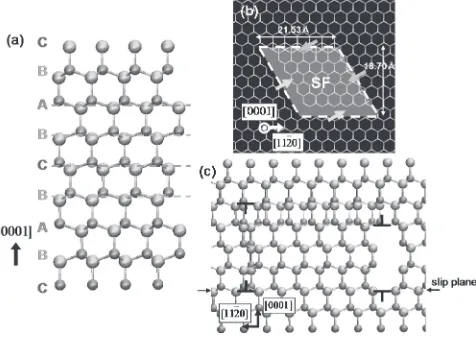
4H-SiC crystal has the periodic structure containing four (ABCB) layers per unit cell, as shown in Fig. 1(a).14)In the
present study, the system in a simulation cell is constructed by duplicating the above structure, and contains 9,600 atoms. The simulation cell has dimensions of 3.95 nm long, 4.30 nm wide and 5.06 nm depth. The periodic boundary condition is applied to the system simulated. In the defect structure proposed from the EBIC and CL experiments,5,6) a basal dislocation of the Burger’s vector b¼1=3½11220 is disso-ciated into two partials with b1¼1=3½10110 and b2¼
1=3½01110, accompanying an extension of a SF regions
between these partials. To model the defect structure, some atoms within a rhombohedral region surrounded by four {1000} and two (0001) planes are shifted along b1. This
creates partial-dislocation loop on (0001) planes with two symmetric Burger’s vectors, b1 and b1, as depicted in
Fig. 1(b). We adopt this model, instead of creating both b1
andb2, because having the full dislocation in the simulation
cell requires extra (or missing) atomic layers in the loop regions. The existence of such layers induces the large strain in entire region of the cell, which is turned out to be fatal in evaluating the net effect of the partials and SFs individually on the electronic structure (e.g., the local DOS outside the loop region may be shifted significantly due to the strain).
In this paper, the areas where atoms reside on and near the partial dislocation cores, accompanied by left-pointing arrows in Fig. 1(b) are denoted as ‘‘high-density area’’, and the area on and near the other dislocation cores are ‘‘low-density area’’, respectively.
4. Relaxed Structure
Figure 2 shows the local structure in the high-density area before and after molecular-dynamics relaxation. While anomalous C-C bonds, which connect electronically having finite values of the bond order between them, are observed before the relaxation (Fig. 2(a)), those bonds disappear after the relaxation (Fig. 2(b)). Furthermore, the atomic structure around dislocation loops are composed of a six-membered ring similar to that of bulk structure, as shown in Fig. 2(c). At the low-density area, on the other hand, there are no significant changes of the atomic structure by the relaxation.
5. Mulliken’s Charge Analysis
Figure 3 shows effective charge transfers of atoms in the system after the relaxation. The effective charge transfer is calculated from the Mulliken’s method10,15)for the electron
population at each atomic site. The color of each atom represents deviation of the charge from its bulk value. Compared with the result of bulk state, the silicons in the low-density area tend to lose electrons, while carbons in the area tend to attract them, indicated by small arrows in the left of Fig. 3, for example. On the other hand, the carbons in the high-density area lose electrons. In addition, the silicons on the½11220dislocation line tend to lose electrons, while others
Fig. 1 Structures of the defect model. Large and small balls represent silicon and carbon atoms, respectively. (a) Perfect 4H-SiC crystal viewed from the direction. (b) Dislocation loop and stacking fault viewed from the [0001] direction. (c) Slip plane viewed from the parallel direction.
[image:2.595.308.546.75.244.2] [image:2.595.315.541.314.358.2]get them, indicated by small arrows in the right of Fig. 3, for example. These results indicate that the electrons in the high-density area have tendency of being displaced along the direction of large arrows in Fig. 3.
6. Density of States
We have evaluated the electronic DOS of the 4H-SiC system which contains dislocation loops using a kernel polynomial method.16)Figure 4 shows a comparison between the DOS in the bulk crystal, in the system with the defects before the relaxation, and that after the relaxation. As shown in Fig. 4(a), the bulk gap Eg obtained from this TB model
is 3.2 eV, which is very close to the experimental value 3.3 eV.5) In the case of the system with dislocation loops,
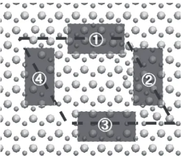
[image:3.595.353.498.67.514.2]the gap state appears before the relaxation, as indicated by an arrow in Fig. 4(b). After the relaxation, however, that state disappears, as shown in Fig. 4(c). To find causes of this phenomenon, the local DOSs in four areas indicated in Fig. 5 are calculated.
Figure 6 shows the local DOSs of two areas in the high-density area before and after the relaxation. In these Figs., the gap state appears at 1.3 eV below the conduction band edge in the bulk gap region before the relaxation, and it disappears after the relaxation. It is assumed that this change is related to the change in bonding network induced by the relaxation as discussed in Sec. 4, that is, the peak in the gap region is related to the abnormal C-C bonds formed before the relaxation. Thus, this peak disappears after the relaxation with the disappearance of those abnormal bonds.
Similarly, Fig. 7 shows the local DOSs of two areas in the low-density area before and after the relaxation. As shown in Figs. 7(a) and (b), there are no peaks in the gap in the area 3 both before and after the relaxation. On the other hand, in the area 4, the gap state appears at shallow level in the gap both before and after the relaxation, as shown in Fig. 7(c) and (d). As in the case of the high-density area, this peak may be attributed to bonding states in the areas. There are dangling bonds in the area 4, whereas there are not in the area 3. In addition, those structures in the area 4 still exist even after the relaxation. This implies that the peaks observed in Fig. 7(c)
Fig. 3 Differential charge transfers of atoms on the dislocation loop and the stacking fault. Large and small balls represent silicon and carbon atoms, respectively. See text for explanations on arrows.
Fig. 4 Electronic DOSs of (a) the bulk crystal, (b) the system which contains the dislocation loop before the relaxation and (c) that after the relaxation.
[image:3.595.56.282.72.234.2] [image:3.595.334.519.597.757.2]Fig. 6 Local DOSs of the high-density area. Inset is the close-up of highlighted area in the figure: (a) Area 1 before the relaxation; (b) area 1 after the relaxation; (c) area 2 before the relaxation; (d) area 2 after the relaxation.
[image:4.595.138.466.71.391.2] [image:4.595.139.460.439.758.2]and (d) are induced by dangling bonds in the area 4. Furthermore, although the present model takes only theb1
partial dislocation loops into account, the area 4 can be considered as the part of the dislocation loop observed in EBIC and CL experiments. Therefore, the peak appeared 0.1 eV below the conduction band edge may correspond to the defect state observed 0.3 eV below the conduction band in EBIC and CL experiments.6)
7. Conclusions
Using a linear-scaling TB simulation, we investigated local structure and electronic states of partial dislocation loop and stacking faults in 4H-SiC. We find that the initial configuration that involves unstable C-C networks around the dislocation loop is relaxed to a structure having six-membered rings, and that the distribution of electron populations is inhomogeneous on the loop. The local electronic density of states shows two peaks in the bulk bandgap, where one of these peaks may correspond to the defect state observed in EBIC and CL experiments.
As discussed briefly in Sec. 3 and 6, the present model deals only one type of the partials proposed in the experi-ments. Also, we have observed a weak appearance of a gap state in the area containing no defects in the system. This may be attributed to the interaction between the defects in the simulation cell and those in the image cells. Analysis with larger simulation cell is therefore inevitable in order to investigate the local electronic states in the system with full types of dislocations and SFs more thoroughly. The simu-lations with several tens of thousands of atoms in a MD cell are in progress.
Acknowledgments
This work was supported by Grant-in-Aid for Scientific Research on Priority Areas ‘‘Nano Materials Science for Atomic Scale Modification 474’’ from MEXT of Japan.
REFERENCES
1) L. Torpo, T. E. M. Staab and R. M. Nieminen: Phys. Rev. B65(2002) 085202.
2) K. Kojima, H. Okumura, S. Kuroda and K. Arai: J. Cry. Growth269
(2004) 367–376.
3) K. Wada, T. Kimoto, K. Nishikawa and H. Matsunami: J. Cry. Growth
291(2006) 370–374.
4) B. Chen, T. Sekiguchi, T. Ohyanagi, H. Matsuhata, A. Kinoshita and H. Okumura: J. Appl. Phys.106(2009) 074502.
5) K. Maeda: Mater. Res. Soc. Symp. Proc.1195(2010).
6) B. Chen, J. Chen, T. Sekiguchi, T. Ohyanagi, H. Matsuhata, A. Kinoshita, H. Okumura and F. Fabbri: Appl. Phys. Lett.93(2008) 033514.
7) M. P. Allen and D. J. Tildesley: Computer Simulation of Liquids, (Oxford, Clarendon, 1989) p. 81.
8) M. P. Allen and D. J. Tildesley: Computer Simulation of Liquids, (Oxford, Clarendon, 1989) p. 149.
9) K. Tsuruta, H. Totsuji and C. Totsuji: Phil. Mag. Lett.81(2001) 357– 366.
10) K. Tsuruta: J. Nanomaterials2011(2010) 308595.
11) S. Goedecker and L. Colombo: Phys. Rev. Lett.73(1994) 122. 12) A. F. Voter, J. D. Kress and R. N. Silver: Phys. Rev. B53(1996) 12733. 13) J. L. Mercer: Phys. Rev. B54(1996) 4650.
14) W. Y. Ching, Y.-N. Xu, P. Rulis and L. Ouyang: Mater. Sci. Eng. A422
(2006) 147–156.
15) R. S. Mulliken: J. Chem. Phys.23(1955) 1833.
16) R. N. Silver, H. Roeder, A. F. Voter and J. D. Kress: J. Comput. Phys.