Abstract— The comprehensive Ando’ surface roughness (SR) model is implemented for nMOSFETs. Four distinct source terms contribute in SR scattering. Relative strength of these contributing source terms are evaluated and compared. The most influential term turned out to be due to scattering with the “physical steps” at the interface. Remote SR scattering is also significant in ultra-thin MOS structures. The proposed model of Gámiz et al for remote SR scattering is studied. It is shown that modification to the Gámiz model is necessary in order to observe the full impact of rms height of the abrupt “steps”.
Index Terms— Surface, Remote Roughness, ultra-thin MOSFET, Mobility.
I. SURFACE ROUGHNESS SCATTERING
part from electron-phonon scattering the most damaging effect to charge carrier mobility in MOS structures is scattering at the rough insulator/substrate interface. This scattering is particularly dominant at high inversion densities, however, due to its nature, it weakly depends on lattice temperature variation. Theoretical models of interface scattering date back to 1968, when Prang and Nee performed simulations to quantify the irregularities of a rough surface [1]. This was followed by a model with explicit mobility dependence on the transverse effective field by Matsumoto and Uemura, which is still adopted today for its simplicity [2]. But a more complete and comprehensive theory is by T. Ando which is by far the best available model regarded by the researchers [3], [4].
According to Ando’s argument there are two main sources of surface roughness scattering affecting the charge carrier’s motion, viz. [3], [4]:
Fluctuation of wavefunctions due to physical “steps” at the interface ((1)).
Fluctuation in potential energy due to Coulomb interactions.
The effects of “change in the potential energy” are further classified as
Change in image potential ((2))
Creation of interface polarization charges ((3)) Fluctuation in charge carrier densities (4)
Matrix element associated with change in wavefunctions is given by [5], [6]:
a) Work done at De Montfort University, Leicester, UK, email:
b) EEE Department, The University of Sheffield, UK, email:
0 ) 1 (
,
dz z z
z E
dz z z
z E dz z z
z V z
j i j
i j i j
i j i
(1a)
where i and j stand for initial and final subbands of a conduction valley, respectively, Ei is the eigenvalue corresponding to the wavefunction i. The potential well in the substrate is denoted by V (in units of energy e.g. eV).
Next among the “Coulomb pieces” i.e. SR induced charge fluctuations---: the scattering potential associated with the second term ((2) ) appears due to the mismatch of the dielectric constants of the two materials (Si and SiO2) across the interface. This effect induces image potential; the corresponding scattering matrix for the change in image potential is given by [7]:
K
qz z dzqz qz K z q
e
q i j
s j
i
0
0 1
2 2 ) 2 (
, 2
~ 16
~
(1b)
where ~
s ox
s ox
with s and ox as the dielectric constants of the substrate and the oxide, respectively. K0andK1 are modified Bessel functions of the second kind and of order zero and one, respectively.The third Coulomb interaction ((3)) is also related to the difference in dielectric constants of the adjacent materials. An extra polarization charge is formed which changes the electric field distribution [3]. The matrix element pertaining to (3) is
given by [5], [7]:
q e i
z
Eeffe qz
j
z dz ji
0 )
3 (
, ~ (1c)
where eis the electronic charge and Eeff is the effective field at the substrate side of the interface.
Lastly, the fluctuations at the interface also affect the electron distribution normal to the interface ((4) term). The redistributed electron charges give rise to an additional scattering potential whose matrix element is [5], [8]:
0 0 2 )
4 ( ,
) ( ~
) ( ) ( 2
) (
z d z
z n e
e
dz z z q
e q
z z q z
z q
j i s j
i
(1d)
where n
z is the volume density of electrons along the z-direction (normal to the interface). With four differentScattering at MOS Interfaces
a)
Raheel Shah and
b)M. M. De Souza
source terms contributing in SR scattering, an “effective” matrix element is required whose squared value could be plugged in the scattering rate (see (3) below). The squared effective scattering matrix i,j(q) is thus, constructed by adding up the squared values of all individual terms (1a-1d) i.e.
2 ) 4 (
, 2 ) 3 (
, 2 ) 2 (
, 2 ) 1 (
, 2
,j(q) ij i j (q) i j(q) i j (q)
i
(2)
In other words each source term in SR scattering is assumed to be uncorrelated to each other and thus contribute independently in mobility degradation. The momentum relaxation rate with the “net” matrix element i,j(q) is given by [9], [10].
) (
) cos 1 ( ) ( 2
) (
1 2
2
0
2 , ) 2 (
,
j j
i d SR
j i
E E
d q
S q
q g
E
(3)
where, E is the total electron energy, g(2d) is the two-dimensional density of state. The Heaviside step function is denoted by (x), while
is the angle between initial and final wave vectors.
q is the static dielectric function of the substrate, introduced in order to account for the screening effects [11]. S
q 2is the “Power Spectrum Density” function given by, (for an exponential autocovariance form [9]):2 3 2 2 2 2 2
) 2 / 1
( )
(q q
S
where is the rms height of the random interface “steps” and is the average width of the same fluctuation.
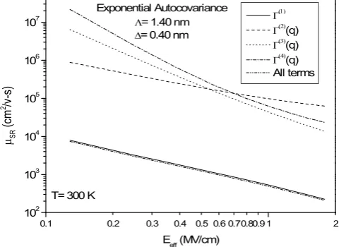
Fig. 1 is a compilation of the results for SR mobility with the effects of individual scattering terms and with their combined influence.
It is clearly evident that the most dominant scattering source is due to the perturbations in electron wavefunctions ((1)). The weakest source is the variation of electron density due to physical “steps” introduced i.e. (4)(q) , though computationally it is a most time consuming term to evaluate.
0.1 0.2 0.3 0.4 0.5 0.6 0.70.80.91 2
102
103
104
105
106
107
Exponential Autocovariance
= 1.40 nm
= 0.40 nm
T= 300 K
SR
(c
m
2/v
-s
)
Eeff (MV/cm)
(q)
(q)
[image:2.595.306.547.218.391.2](q) All terms
Fig. 1: Relative strengths of four sources of SR scattering are compared. The most damaging source for channel mobility is the
) 1 ( ,j i
term.
The percentage difference between mobility computed with all terms and then with (1)+
(2)(
q
)
+(3)(q)terms isaround 1% at Eeff 1MV/cm. Thus these three terms are sufficient to account for SR scattering and (4)(q) can be safely ignored.
Unlike phonon limited mobility the temperature dependence of SR scattering is very weak. Theoretically the temperature term appears in the formulation via the Fermi-Dirac distribution. Variation of SR mobility at two different effective field values over the temperature scale is shown in fig 2. As expected the small exponent of `T` indicates the weak temperature dependence of SR scattering.
80 90 100 200 300 400 500
200 300 400 500 600 700 800 900 1000 2000 3000
= 1.40 nm
= 0.40 nm
Eeff ~0.5 MV/cm Eeff ~1.0 MV/cm
T-0.47
T-0.26
SR
(c
m
2/V
-s
)
Temperature (K)
Fig. 2: Weak SR temperature dependence is shown. Redistribution of electron via Fermi-Dirac function introduces temperature dependence in SR scattering.
At very low temperatures the effect of phonon scattering is minimum and thus only surface roughness scattering contributes towards the effective mobility in the region of medium to high transverse field. Simulations are performed at T=77 K and the results are compared with the measured mobility extracted from ref. [12], in fig. 3. With the chosen and values, simulated mobility successfully follows the measured mobility and its temperature dependence trend (Eeff1.71).
0.4 0.5 0.6 0.7 0.8 0.9 1.0
0 500 1000 1500 2000 2500
Eeff-1.71
SR
(c
m
2/V
-s
)
Effective Field (MV/cm) T= 77 K
Circles: Measured Data Line: Simulations
Source Terms
(q)=(1)
+(2)
(q)+(3)
(q)
= 1.40 nm
[image:2.595.304.547.566.742.2]= 0.40 nm
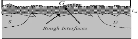
[image:2.595.47.289.569.744.2]II. REMOTE SURFACE ROUGHNESS SCATTERING Another scattering mechanism, closely related to SR scattering, is the “Remote Surface Roughness” (RSR) scattering. For ultra thin oxide layered MOS structures, charge carriers in the channel can significantly dissipate their momentum by remotely interacting with the gate/insulator interface. Similar to oxide/substrate interface the second interface i.e. gate/oxide interface is not smooth and deviates from the ideal plane, as shown in fig. 4. Degree of roughness at the two interfaces is uncorrelated and depends on the device processing mechanism.
Fig. 4: Deviation from ideal surfaces is shown for gate/insulator and insulator/substrate interfaces. Both interfaces are assumed
uncorrelated.
A. RSR Model Equations
Extending the concept first presented by Li [13], Gámiz et al proposed a simple scattering model for the remote surface roughness mechanism [14], [15]. In their proposed model the Hamiltonian of the system is given by:
r m z V H
H 0 ( ) (4)
where: ) ( ) ( )
(z V z V0 z
V tox m
(5)
with Vtoxm as the perturbed potential in the presence of
“steps” at the gate/insulator interface while V0 is the unperturbed potential i.e. in the case of ideal boundary. Surface topology is measured via 2D roughness function,
r , which describes the fluctuations from an assumed ideal flat boundary. The two- dimensional vector r is measured along the interface plane. H0 is the initial unperturbed Hamiltonian and the final Hamiltonian H arising from the change in potential energy along the z-direction. The rms value of the step height at the second interface is denoted bym. Using the Hamiltonian (4) the matrix element was constructed as [14]:
0
, (z) V(z) j(z)dz m
i RSR
j
i (6)
The matrix element (6) modulated by dielectric function )
(q
is plugged in (3) to compute the RSR scattering rate. However, Hamiltonian (4) of the present system can also be utilized to construct a relatively better RSR matrix element, following the approach described below:
Consider the change in the Hamiltonian of the system due to the presence of a random “step” at the interface, given by:
0
H H H
(7)
Next the matrix element for the changed Hamiltonian is generated from equation (7):
z
H
z dz dz z H z j i j i j i 0 0 0 0 ,
r r r
(8)
Note that for the final Hamiltonian H, the final perturbed wavefunctions are used. Substituting equation (4) in (8) to get:
z
H
z dzdz z z V H z j i j m i j i 0 0 0 0 0 , ) (
r r r r
(9)
Next using Taylor’s theorem for the expansion of the wavefunctions to the lowest order reveals:
dz
z
H
z dzz z z z V H z z z j i j j m i i j i 0 0 0 0 0 , ) (
r r r r (10)Ignoring the product terms involving
r 2:
z
H
z dzdz z z z H z z V z z z z H z H z j i i j j m i j i j i j i 0 0 0 0 0 0 0 , ( )
r r r r (11)Now, from the time independent Schrödinger equation:
E
H0 (12)
Equation (11) is modified using (12) and after simplification the net result is:
dzz z z E z z z E z z V z i j i j i j j m i j i
0 0 , ) ( ) ( r r (13)
RSRj i j
i0, ( ) ,
r r (14)
where,
0 , dz z z z E dz z z z E dz z z V z i j i j i j j m i RSR j i (15)is the modified form of the matrix element given earlier in equation (6).
scattering [1]. The matrix element given in (6) over estimates the RSR limited mobility as compared to one in computed using (14). Another shortcoming of the Gámiz model is that the effect of rms m is not present explicitly (it cancels out in the scattering rate when squared matrix element is multiplied with power spectrum S(q)2). The only weak dependence of
m
appears in Gámiz model is through simulated value of )
(z V
(via the coupled Schrödinger Poisson solver) in (6), while the modification presented here to the transport model includes m explicitly and thus its effect is realistically observed.
For comparison, results obtained using the two model equations are shown in fig. 5. In this study, two different theoretical values of m (0.5nm and 0.3nm) are used for a fixed oxide thickness of 1.0nm. Potential V(z) in (5) with wavefunctions and eigenvalues are computed using UT-Quant Schrödinger-Poisson solver [16]. With
nm m 0.5
, the drop from the “Universal mobility” is around 5% at
cm MV Eeff ~1 .
0.2 0.4 0.6 0.8 1.0 1.2 1.4 1.6
3.0x10³
6.0x10³
9.0x10³
1.2x10⁴
1.5x10⁴
tox=1.0 nm =1.3 nm T= 300 K
m=0.30 nm
m=0.50 nm
Solid: Gamiz Model Broken: This Work
RSR
(c
m
2 /V
-s
)
[image:4.595.305.547.48.224.2]Eeff (MV/cm)
Fig. 5: RSR limited mobility computed using Gámiz et al model [14] and the modified model proposed in this work. Gámiz model overestimates the mobility as compared to the new model.
B. Observed trend in RSR mobility
From fig. 5 two observations can be clearly made, first: smoother the surface (smallm) better is the RSR limited mobility. The reason for this behaviour is obvious. Secondly: Initially RSR mobility increases with increasing sheet density,
s
N , after reaching to an absolute maximum, mobility then starts declining. Possible reasons for this trend are explored below.
The scattering potential, which is in fact the difference in perturbed and unperturbed potentials (V (z) V0(z)
m ox
t ),
decreases with evolving sheet density, Ns. Fig. 6 illustrates this fact graphically. Additionally, screening also contributes towards mobility enhancement. On the other hand, with increasing transverse field, the wavefunctions are more squeezed towards the interface and thus magnitude of the matrix element increases, consequently lowering the mobilities (see (6) or (15)). At the maximum (“breakeven
0 5 10 15 20 25
0.000 0.005 0.010 0.015 0.020 0.025
Ndop=3x10¹⁷
(cm-3
)
T= 300 K tox=1.0 nm m=0.15 nm
Po
te
nt
ia
l
(Vtox
+
m
-
V0
)
(V
ol
ts
)
z depth (nm)
Ns~1x10¹²
(cm-2
) Ns~1.5x10¹³ (cm-2)
Fig. 6: Difference in the unperturbed and perturbed potentials are plotted for two different sheet concentrations. For strong inversion
the difference in potentials V(z) drops sharply.
point”), observed in fig. 5, the two effects i.e. V(z) and the “squeezing wavefunctions” just balance each other. Beyond this point, a further increase in gate voltage favours the impact of squeezed wavefunctions and thus mobility starts dropping, similar to the trend observed in “normal” SR mobility.
It is appropriate here to comment on comparison made by Saito et al [17] for RSR mobility with the reported results of Gámiz et al [14]. In their conclusion, apparent “contradiction” is reported from the perspective of the effective field region, where the RSR scattering is more dominant. In simulations performed by Saito et al, impact of RSR scattering is strong in the high effective field region; while according to Gámiz model low effective field regime is important for RSR scattering. However, results presented here resolve the apparent “discrepancy” and conclusively show that RSR scattering mechanism is strong in both low and in high transverse field regimes.
III. CONCLUSION
[image:4.595.46.290.210.511.2]REFERENCES
[1] R. E. Prange and T. W. Nee, "Quantum spectroscopy of the
low-field oscillations in the surface impedance," Physical
Review, vol. 168, pp. 779-786, 1968.
[2] Y. Matsumoto and Y. Uemura, "Scattering mechanism and low
temperature mobility of MOS inversion layers," in Japanese
Journal of Applied Physics, suppl.2, pt.2, Kyoto, Japan, 1974,
pp. 367-70.
[3] T. Ando, "Screening effect and quantum transport in a silicon
inversion layer in strong magnetic fields," Journal of the
Physical Society of Japan, vol. 43, pp. 1616-26, 1977.
[4] T. Ando, A. B. Fowler, and F. Stern, "Electronic properties of
two-dimensional systems," Rev Mod. Phys, vol. 54, pp.
437-672, 1982.
[5] J. Seonghoon, M. V. Fischetti, and T. Ting-Wei, "Modeling of Surface-Roughness Scattering in Ultrathin-Body SOI
MOSFETs," Electron Devices, IEEE Transactions on, vol. 54,
pp. 2191-2203, 2007.
[6] D. Esseni, "On the modeling of surface roughness limited mobility in SOI MOSFETs and its correlation to the transistor
effective field," Electron Devices, IEEE Transactions on, vol.
51, pp. 394-401, 2004.
[7] M. V. Fischetti and S. E. Laux, "Monte-Carlo Study of
Electron-Transport in Silicon Inversion-Layers," Physical
Review B, vol. 48, pp. 2244-2274, 1993.
[8] M. V. Fischetti, Z. Ren, P. M. Solomon, M. Yang, and K. Rim,
"Six-band k.pcalculation of the hole mobility in silicon
inversion layers: Dependence on surface orientation, strain,
and silicon thickness," Journal of Applied Physics, vol. 94, pp.
1079-1095, Jul 15 2003.
[9] S. M. Goodnick, D. K. Ferry, C. W. Wilmsen, Z. Liliental, D. Fathy, and O. L. Krivanek, "Surface roughness at the
Si(100)-SiO2interface," Physical Review B, vol. 32, p. 8171,
1985.
[10] D. K. Ferry and S. M. Goodnick, Transport in Nanostructures:
Cambridge University Press, 1999.
[11] D. Esseni and A. Abramo, "Modeling of electron mobility degradation by remote Coulomb scattering in ultrathin oxide
MOSFETs," Electron Devices, IEEE Transactions on Electron
Devices, vol. 50, pp. 1665-1674, 2003.
[12] S.-i. Takagi, A. Toriumi, M. Iwase, and H. Tango, "On the universality of inversion layer mobility in Si MOSFET's: Part
II - effects of surface orientation," IEEE Transactions on
Electron Devices, vol. 41, pp. 2363-2368, 1994.
[13] L. Jia and T. P. Ma, "Scattering of Silicon Inversion Layer
Electrons by Metal-Oxide Interface Roughness," Journal of
Applied Physics, vol. 62, pp. 4212-4215, Nov 15 1987.
[14] F. Gamiz and J. B. Roldan, "Scattering of electrons in silicon
inversion layers by remote surface roughness," Journal of
Applied Physics, vol. 94, pp. 392-399, 2003.
[15] F. Gamiz, A. Godoy, F. Jimenez-Molinos, P. A. C.-C. P. Cartujo-Cassinello, and J. B. A. R. J. B. Roldan, "Remote surface roughness scattering in ultrathin-oxide MOSFETs," in
European Solid-State Device Research, 2003. ESSDERC '03.
33rd Conference on, 2003, pp. 403-406.
[16] S. J. W.-K. Shih, G. Chindalore, " UTQUANT 2.0 User's
Guide," University of Texas Press, Austin, 1997.
[17] S. Saito, K. Torii, Y. Shimamoto, S. Tsujikawa, H. Hamamura, O. Tonomura, T. Mine, D. Hisamoto, T. Onai, J. Yugami, M. Hiratani, and S. Kimura, "Effects of remote-surface-roughness scattering on carrier mobility in field-effect-transistors with
ultrathin gate dielectrics," Applied Physics Letters,vol. 84, pp.
![Fig. 5: RSR limited mobility computed using Gámiz et al model [14]and the modified model proposed in this work](https://thumb-us.123doks.com/thumbv2/123dok_us/1312926.661425/4.595.46.290.210.511/limited-mobility-computed-using-gamiz-model-modified-proposed.webp)
