warwick.ac.uk/lib-publications
A Thesis Submitted for the Degree of PhD at the University of Warwick
Permanent WRAP URL:
http://wrap.warwick.ac.uk/110577/
Copyright and reuse:
This thesis is made available online and is protected by original copyright.
Please scroll down to view the document itself.
Please refer to the repository record for this item for information to help you to cite it.
Our policy information is available from the repository home page.
C H A R A C T E R ISA T IO N OF HI-V Q U A T E R N A R Y
M
u l t i l a y e r
s e m i c o n d u c t o r
d e v i c e
m a t e r i a l s
B Y X -R A Y D IFF R A C T IO N
A thesis submitted to the University o f Warwick for the degree of Doctor o f Philosophy
by
S. Swaminathan
Department of Engineering
University o f Warwick
February, 1985
I , 1
O C i i e s
*.» U »
SUMMARY
Optoelectronic devices find extensive use in optical fibre conununication systems as infrared sources, in view of a relatively low attenuation of the optical fibres for such sources in the spectral range 1.0 - 1.4 pm. In the study of optoelectronic device materials, minute variations in the lattice parameter of different layers cause lattice strain, which, along with other factors namely thermal gradients, a high density of recombining carriers in the active layer promote the motion, multiplication and growth of defects into network clusters.
In this thesis a double crystal plane wave synchrotron radiation technique has been found to be capable of accurately characterizing individual layers in a multilayer structure such as in an opto electronic device consisting of many layers of InGaAs, InGaAsP and InP grown over an InP substrate. This non-destructive method can separate images of the ternary and quaternary layers from the substrate (InP) thereby identifying the location of any defects as well as detailed^identification of dislocation-type defects. The observed presence of a cross hatch pattern of interfacial misfit dislocations has been strongly correlated to the degradation of the device. The technique also enables a very precise plot of the rocking curves which provides invaluable information about the assessment of the thickness, compositional variation in the ternary or quaternary epitaxial layers and also of their crystalline
perfection. The technique is capable of mapping lattice parameter differences of the order of 10- ®. A fairly accurate assessment of the inhomogeneity and non uniformity of quaternary multilayers grown by liquid phase epitaxy has been made by this technique. About 54Z variations in the total quaternary layer thickness was observed for a double heterostructure laser and about 39Z for a thick graded single layer quaternary specimen.
For multilayer structures showing complicated rocking curves, it has been demonstrated that a selective etching of the layers in sequence helps identify the individual layer characteristics. A theoretical calculation of rocking curves from heteroepitaxial layers is presented. Initial data from experimental rocking curves are used to calculate rocking curves for the multilayer structure and then compared with experimental curves. The input data are slightly adjusted about their initial values until a reasonable fit with experimental curves is achieved. The initial data consist of
the knowledge of the thickness and mismatch variations of each layer in the multilayer structure. The mismatch variations for the layers as obtained by selective etching have been effectively used to simulate experimental rocking curves. An accurate interpretation of layer characteristics from such a simulated fit has thus been made possible. Simulation studies have thus been found to offer a powerful and non destructive method of a detailed and accurate assessment of layer thickness and compositional variations by comparison with
experimental rocking curves. Studies on a number of specimens have shown satisfactory agreement: the predicted thicknesses
I
CONTENTS
INTRODUCTION 1
Page N o .
REVIEW OF THE METHODS OF ASSESSMENT OF III-V SEMICONDUCTOR DEVICE MATERIALS
2.1. Introduction 12
2.2. Assessment of Microstructures 13 2.2.1. Optical Microscopy 13
2.2.2. Transmission Electron Microscopy 16 2.2.3. Scanning Electron Microscopy 22 2.2.4. X-ray Topography 26
2.3. Microanalytical Techniques 32
2.3.1. Electron-probe Microanalysis 32 2.3.2. Auger Electron Spectroscopy 35 2.3.3. Secondary Ion Mass Spectrometry 36 2.4. Discussions 36
References
EPITAXIAL GROWTH OF GalnAsP/InP SYSTEMS
3.1. Introduction
^6
3.2. Liquid Phase Epitaxy 46 3.2.1. The Apparatus 51 3.2.2. The Growth 54
3.2.3. Features of the Growth 56 3.3. Vapour Phase Epitaxy 57
3.4. Metal-organic Chemical Vapour Deposition 59 3.5. Molecular Beam Epitaxy 61
3.6. Discussions 62 References
DYNAMICAL THEORY OF X-RAY DIFFRACTION
4.1. Introduction 70
4.2. The Laue Condition 72
4.3. Periodic Complex Dielectric Constant 73 4.4. Solutions to Maxwell's Equations 75 4.5. Boundary Conditions for Solutions
of Maxwell's Equations 81
4.6. Pende U S e u n g 82
4.7. Rocking Curve Profiles 85 4.8. Distorted Crystels 86 4.9. Discussions 91
I
Page No
DOUBLE CRYSTAL EXPERIMENTAL METHODS 9 3
5.1. 5.2. 5.3. 5.4. 5.5.
Introduction 93 The Source 94 Beam Conditioner 96
The Double Crystal Camera 99 Detectors and Counters for
Topography and Rocking Curves 104 5.5.1. Plot of Rocking Curves 106 5.5.2. Recording of Images 108 5.6. Discussions 109
References
DOUBLE CRYSTAL ROCKING CURVES AND TOPOGRAPHS OF OPTO
ELECTRONIC DEVICES AND MULTILAYER STRUCTURES AND THEIR 112 INTERPRETATION
6
.1
.6
.2
.Introduction 112
Characteristics of the Silicon Monochromator 112
6.3. 6.4.
Experimental Results 113 Discussions 129
References
AREA SCANNING OF ROCKING CURVES TO ASSESS EPILAYER 133 PROPERTIES
7.1. 7.2.
Introduction 133
A Double Heterostructure Laser, Specimen M979 134
7.2.1. Experimental Procedure 134 7.2.2. Assessment of Composition 145 7.2.3. Assessment of Thickness 147 7.3. A Linearly Graded Quaternary Single
Layer, Specimen L5 149 7.4. Discussions 153
References
CHARACTERISATION OF A DOUBLE HETEROSTRUCTURE LASER AND 158 AN EDGE EMITTING LED BY SELECTIVE ETCHING
Introduction 158
Experimental Procedure 159 Discussion 173
References
8
.
1.
8.
2.
r
INVESTIGATION OF THE CHARACTERISTICS OF AN EPITAXIAL 178 LAYER AT DIFFERENT STAGES OF ITS GROWTH
9.1. Introduction 178
9.2. Experimental Methods and Results 178 9.2.1. Samples with Growth Terminated at Intermediate Stages 179 9.2.2. Sample Etched Off to Various
thicknesses 183 9.3. Discussion 192
Page N o .
COMPUTER SIMULATION OF ROCKING CURVES AND THEIR COMPARISON 193
WITH EXPERIMENTAL CURVES
10.1. Introduction 193
10.2. Calculation of Rocking Curves 194 10.3. Determination of Structure Factors 196
10.3.1. Alloy Composition x and y 197 10.3.2. Dispersion Corrections for
Atomic Scattering Factors 199 10.3.3. Atomic Scattering Factors 200 10.4. Effect of Tetragonal Distortion on
the Epitaxial Layer Mismatch 201 10.5. Rocking Curve Simulation 203
10.5.1 Single Epitaxial Layers of Uniform Composition 204 10.5.2. Single Epitaxial Layers of
Varying Composition 215
10.5.3. Epitaxial Multilayer structures 216 10.6. Theoretical Fitting of Experimental
Rocking Curves 225
10.6.1. A Double Heterostructure Laser, R154 225 10.6.2. A Double Heterostructure Laser, M979 233 10.6.3. Linearly Graded Quaternary Single
Layer, Specimen L5 242 10.6.4. Etched Single Layers of Linearly
Graded Quaternary Specimen, L5 248 10.6.5. A Light Emitting Diode, VS296A 260 10.7. Discussion 260
References
1.1. A schematic diagram of a typical GalnAsP/InP heterostructure laser. The oxide-stripe
geometry and the antimelt back layer are for 3 the 1.5 - 1.67pm wavelength emission
1.2. The energy band structure of GaAs with energy E
plotted as a function of momentum wave vector k
3
along [100
] and [1 1 1
] directions1.3. Lattice constant variation with bandgap energy
for various III-V alloys. The shaded region 3 represents the quaternary field
1.4. Dependence of the threshold current density on
thickness of the active layer. The experimental
6
points are from the data of Itaya et al(2
)1.5. Schematic representation of misfit dislocations
6
2.1. A sketch of a vertical cross section of a TEM 18 [after Holt(49) ]
2.2. Formation of a micrograph and diffraction pattern 19 in a TEM
2.3. Schematic diagram of a scanning electron, 23 microscope [after Bowen and Hall(17)]
2.4. The various types of energy dissipation 23 constituting different operating modes
of an SEM
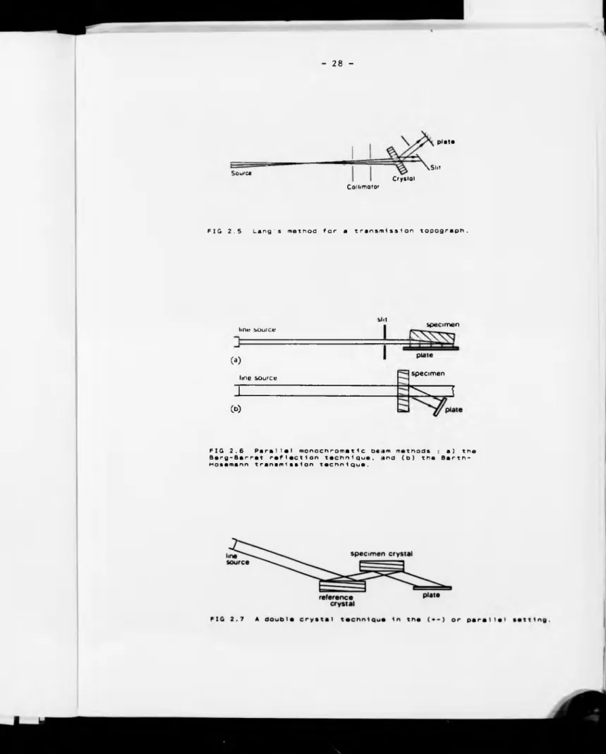
2.5. Lang's method for a transmission topograph 28
2.6. Parallel monochromatic beam methods :
a) the Berg-Barret reflection technique, and 28 b) the Barth-Hosemann transmission technique
2.7. A double crystal technique in the (+ -) or 28 parallel setting
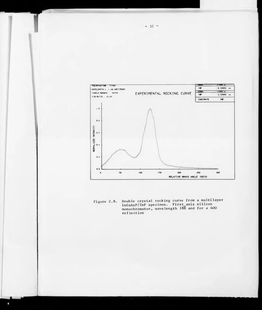
2.8. Double crystal rocking curve from a multilayer
InGaAsP/InP specimen. First axis : silicon mono- 31 chromator. Wavelength : 1.8A and for a
400 reflection
2.9. Block diagram of an electron-probe microanalyser
LIST OF FIGURES
Page N o .
Page No.
3
.
1.
Composition of the liquidus that yield lattice matched GalnAsP alloys by growth at four different temperatures on (a) (100) InP substrates, and (b) (lll)B InP substrates. The symbols refer to the data of the following references : F (Feng et al(7)), N (Nagai and Noguchi (8
)), 0 [Oe and Suglyama (9)], x and +(Perea and Fonstad(15)), (after Hsieh(
6
))S
3.2. The relation between Ga and Ga for growth of lattice matched GalnAsP alloys on (a) (100) InP substrates and (b) (lll)B InP substrates at four different temperatures. The broken lines are those calculated by Perea and Fonstad(15)
3.3. (a) Schematic diagram of the LPE apparatus
(b) The graphite boat with various melts for the growth of a double heterostructure laser
3.4. (a) Liquidus isotherm for the In-Ga-As-P system at As®' = 0.05
£
(b) Solid solubility isotherm for Ga at As = 0.03 and 0.05. The full curves in both the figures are the calculated isotherms while the broken lines are the experimental curves obtained from the daya of Nakajima et al(2.4)
4.1. Construction of a dispersion surface showing the loci of tie points like A, which define wave vectors whose real parts satisfy both Maxwell's equation and the Laue equation when there are only two strong waves
5.1. (a) Spectral curves from a normal bending magnet (1.2T) and from a 4.5T wiggler magnet for a 2 GeV 1A beam in the SRS
(b) Spectral curves transmitted through 380um Be windows on X-ray beam lines
5.2. A schematic diagram of the (111) silicon monochromator. The low and high angles of
incidence are 6.05 and 76.6 degrees respectively.
5.3. The relation between wavelength and incident Bragg angle for the silicon monochromator
5.4. Change in upper and lower wavelength limits with beam size for the silicon monochromator
48 48 52 52 53 53 78 94 94 96 98 98
Page N o .
5.7.
5.8.
6
.
1.
6
.
2.
6.3.
6.4.
6.5.
6.6.
6.7.
6
.
8.
6.9.
6 .1 0
Photograph of the double crystal camera in an experimental set-up. An order sorting beam conditioner is mounted on the right hand fine axis while a test specimen is mounted on a goniometer on the left hand fine axis
A sketch of a typical double crystal experimental arrangement
Block diagram of the control system for a rocking curve plot
Topograph of the silicon monochromator for
111
reflection at l8
wavelengthA schematic diagram of the light emitting diode, VS296A
Double crystal reflection topographs for the specimen VS296A. Wavelength : 1.0&, 400 reflection. (a) Topograph corresponding to the InP peak, (b) Topograph corresponding to the quaternary layer peak
(a) InP and (b) quaternary topographs of the specimen VS296A rotated 90° degrees in its plane. 1.08 wavelength, 400 reflection
White radiation topograph of the InP reference crystal, 400 reflection
Double crystal rocking curve for the specimen VS296A. First axis : InP, 400 reflection and slit size :
100
pm x2
m mDouble crystal rocking curve for the specimen M979. First axis : Silicon monochromator, 400 reflection, slit size, 100pm x 500pm
Rocking curve for M979 with InP as first crystal, 400 reflection and slit size : 100pm x 500pm
Schematic diagram of the double heterostructure laser, M979
Rocking curve for M979 for a different input wavelength. First axis : silicon mono chromator, 400 reflection and slit size : 100pm x 500pm
Page No.
6
.
11.
6
.12
.Double crystal rocking curves for a set of three edge emitting LEDs that had shown degradation effects. First axis : silicon monochromator. Input wavelength : 1.0&,
slit size : 100pm x 500pm
a) specimen M952 shows a quaternary layer peak whose mismatch is graded and positive
b) specimen M949 shows only one peak and is therefore lattice-matched. The peak is however broad
c) specimen M777 also shows only one peak but the peak is much narrower
Double crystal topographs for the three specimens M952, M949 and M777. Wavelength :
l.oS,
400 reflection, First axis : silicon monochromatora) Topograph of the InP peak for M952
b) Topograph of the quaternary peak for M952
c) Topograph of the only observed peak for M949
d) Topograph of the only observed peak for M777
124
126
6.13. Limiting region for lattice mismatch and active layer thickness for initiation of misfit 128 dislocations at the interface. Data points o and x are due to Nakajima et al(3) for several Ga In^ ^As/InP single layer specimens of
different thicknesses. The misfit dislocation- free region is shown by the shaded region.
6.14.
6.15.
6.16.
7.1.
Double crystal rocking curve for the specimen R296A. 400 reflection, First crystal : InP
Double crystal rocking curve for the specimen M980. 400 reflection, First crystal : InP
Double crystal rocking curve for the specimen M978. 400 reflection, first crystal : InP
a) A schematic diagram of the DH laser M979
b) Positions on the top surface of the
specimen where rocking curves were recorded
130
Page No.
7.2. X-Y translation and tilting stage used for scanning the specimen area. The specimen
is placed on the translation table A.
135
X-Y translation is achieved by the steppermotor and micrometer combination (SI, Cl) and (S2, C2) respectively while tilting is achieved by (S3, Z) through a gearbox G. The spindle T slots into the second axis of the double crystal camera.
7.3. Comparison of double crystal rocking curves at various positions on the specimen M979. First axis : Silicon monochromator,
400 reflection, slit size : lOOpra x 2mm
a) at the point A 138
b) at the point B 138
c) at the point C 139
d) at the point D 139
e) at the point E 140
f) at the point F 140
g) at the point G 141
h) at the point H 142
i) at the point I 142
The various positions for rocking curves are indicated in Figure 7.1b
7.4. A schematic diagram of the specimen L5.
The points G, D, E and F refer to the 148 positions where rocking curves were plotted
and compared.
7.5. Comparison of double crystal rocking curves at four positions on the specimen, L 5 . First crystal : InP, 400 reflection. Slit size : 100pm x 500pm
a) at the point G 151
b) at the point D 151
c) at the point E 152
e) at the point F 152
Page No.
7.6. Double crystal reflection topographs of the specimen L 5 . 400 reflection,
Wavelength : 1.5&
a) Topograph of the substrate peak
b) Topograph of the epilayer peak
155
8.1. A schematic diagram of the DH laser, R154 159
8.2. a) Etching configuration for the specimen R154. The upper half of the top surface was divided into four sections
161
b) By masking each window in turn, and using selective etchants, a portion of each layer of the multilayer structure can be exposed. Vertical height in this figure not to scale
161
8.3. Etching rate in InP for the (4 HCZ + HO)etchant at 1°C (after Arai et al(
6
))161
8.4. Comparison of double crystal rocking curves at various positions on the specimen R154. First crystal : InP, 400 reflection, slit size! lOOum x 500vim
a) at the point A 163
b) at the point B 163
c) at the point C 164
d) at the point D 164
e) at the point F 165
f) at the point E 165
g) at the point G 166
h) at the point H
The various points where rocking curves were recorded are shown in Figure 8.2a
166
8.5. A schematic diagram of the edge emitting LED, R249
168
8
.6
. (a) Etching configuration for R249(b) Etched layer arrangement, side view. Vertical height in this figure not to scale
169
Page N o .
8.7. Comparison of double crystal rocking curves at various positions on the specimen R249. First crystal : InP 400 reflection
a) at the point A
b) at the point B
c) at the point C
d) at the point F
e) at the point G
9.1. Double crystal rocking curve for a 400 reflection from a point 100pm x 500pm on a quaternary single
layer specimen. First axis : silicon mono chromator. Input wavelength : 1.5A
a) VS399B has slight asymmetry on its right corresponding to a positive mismatch : could be due to a thin layer
b) VS399A, slightly thicker, *p 500$,has a symmetric rocking curve
c) VS397, around 2pm thick, has asymmetry to the left corresponding to a negative mismatch
9.2. Double crystal reflection topographs for three single layer specimens of different thicknesses at the only peak, observed for each specimen. Incident wagelength : 1.5A, 400 reflection
a) Topograph of VS399B
b) Topograph of VS399A
c) Topograph of VS397
9.3. Experimental arrangement for etching the layer to various thicknesses
(a) Points A to G refer to the positions on each etched window where rocking curves are plotted
(b) A side view of the etching configuration
9.4. Graph showing a variation in the step changes in thickness of the etched layers from one point to another, as plotted by the Talysurf
Page N o .
9.5.
10
.1
a (1 to 4)10
.1
b (1 to 4)10
.2
a (1 to 5)10
.2
b (1 to 4)10.3a (1 to 4)
10.3b (1 to 3)
Double crystal rocking curves at various positions on the etched specimen L 5 . First crystal : InP, 400 reflection,
a) corresponding to position A
b) corresponding to position B
c) corresponding to position C
d) corresponding to position D
e) corresponding to position E
f) corresponding to position F
g) corresponding to position G
The various points where rocking curves were recorded are shown in Figure 9.3a
Effect of increasing layer thickness on simulated rocking curves for a single homogeneous GalnAs epitaxial layer
Effect of increasing layer mismatch on simulated rocking curves for a single homogeneous GalnAs epitaxial layer
Effect of increasing layer thickness on simulated rocking curves for a single homogeneous GalnAsP epitaxial layer. An emission wavelength = 1.245pm corresponding
to band gap energy Eg = 0.996 eV is assumed
Effect of increasing layer mismatch on simulated rocking curves for a single homogeneous GalnAsP epitaxial layer. Emission wavelength = 1.245pm
Effect of increasing mismatch gradient on simulated rocking curves for a single
GalnAsP epitaxial layer with graded mismatch. Emission wavelength = 1.31um. Average
mismatch = 500 ppm
Effect of increasing layer thickness on simulated rocking curves for a single GalnAsP epitaxial layer with a graded mismatch. Emission wavelength = 1.31pm Average mismatch = 500 ppm. Mismatch gradient “
100
ppm/pm10.4. (1 to 3)
10.5.
(1,2)
Effect of increasing number of layers with two levels of mismatch on simulated rocking curves for a multilayer GalnAsP/InP structure. Emission wavelength * 1.31pm. Total thickness of the layers =
2.0
umEffect of increasing the total thickness of the layers on simulated rocking curves for a multi layer GalnAsP/InP structure. Emission wavelength = 1.31pm. Number of layers = 4
10.6. Comparison of the experimental and simulated (a to j ) rocking curves for the specimen R154. Energy
band gap for the buffer layer = 1.35 e V : emission wavelength for the active layer is
1.31pm. Mismatch levels are as indicated in the insets in
thicknesses in are as follows
the graphs, microns, for
The simulated layer the various graphs
Buffer layer Active layer p-InP cap
a 9.0
0.2
1.9 0.15b 9.0
0.2
1.9c
6.0
0.2
d 9.8
0.2
e 9.8
0.2
f 9.8
0.2
g 9.8
0.2
h 9.8
i 9.0
j 9.8
0.2
1.9 0.15222
Page N o .
Page No.
10.7. Comparison of the experimental and simulated (a to 1) rocking curves for the specimen M979. Emission
wavelength for the active layer = 1.31pm. Energy band gap for the quaternary cap is 1.24 eV. Mismatch levels are as indicated in the insets in the graph. The simulated layer thicknesses
as follows
(pm) for the various graphs are
n-InP Q-Active p-InP Q-cap
a
2
0.252
0.6
235b
2
0.252
0.6
235c
2
0.252
0.3+0.3 236d
2
0.502
0.3+0.3 236e
2
0.252
0.2+0.5 237f
2
0.252
0
.2
+0
.7 237g
2
0.252
0
.2
+0.8
238h
2
0.252
0
.2
+0
.9 238i
2
0.252
0 . 3+0.8
239j
2
0.252
0.3+0.7 239k
2
0.252
0
.4+0.8
2401
2
0.252
0.4+0.7 24010.7m Thickness of the ternary cap as measured at three regions using the Talysurf, are 0.95pm, 0.90pm and 0.90pm respectively,
Page No.
10.8. Comparison of Che experimental and simulated (a to j) rocking curves for the specimen L 5 . Emission
wavelength for the layer is = 1.245pm. Mismatch levels are as indicated in the insets in the graphs. The simulated layer thicknesses (pm) for various graphs are as follows
Layer thickness
a 4.2 243
b 4.2 243
c 4.2 244
d 4.0 244
e 4.0 245
f 4.2 245
g 4.1 246
h 3.6 246
i 3.7 247
j 3.8 247
.9. to k)
Comparison of the experimental and simulated rocking curves for the specimen L5 progressively etched to produce layers of varying thicknesses. Emission wavelength for the layer is = 1.245pm. Mismatch levels are as indicated in the insets in the graphs. Simulated thicknesses (pm) for the various graphs are as follows
Layer thickness
a 3.6 250
b 3.35 251
c 3.35 251
d 3.20 25 2
e 3.10 252
f 3.20 25 3
g 3.10 253
h 3.20 25 4
i 3.10 25 4
j 2.80 255
Page N o .
10.10. Comparison of the experimental and (a to h) simulated rocking curves for the
specimen VS296A. Emission wavelength for the active layer is X = 1.31ym.
Energy bandgap of the cap layer is 1.24 eV. Mismatch levels are as indicated in the insets in the graphs. Simulated layer thicknesses (pm) for various graphs as
as follows
N-InP Q-Active p-InP Q-cap
a
2
2
1
0.25 261b
2
2
1
0.25 261c
2
2
1
0.50 262d
2
2
1
0.25 262
e
2
2
1
0.50263
f
2
2.51
0.50 263g
2
2.51
0.50 264LIST OF TABLES
Page N o .
2
.
1.
2
.
2
.
6.1.
6
.
2.
7.1.
7.2.
7.3.
7.4.
8
.
1.
8
.
2.
9.1.
9.2.
Information available from various operational modes of SEM
A comparison of microanalytical techniques
Comparison of rocking curve characteristics for a double heterostructure laser for different incident beam wavelengths and different reference crystals on the first axis of the double crystal camera
Comparison of the InP and quaternary layer characteristics for a set of three edge emitting LEDs from their corresponding rocking curves of Figure 6.11
Characteristics of InP and InGaAsP layers from experimental rocking curves for the DH laser, M979. Wavelength : 1.88, 400 reflection
Assessment of x and y composition for In Ga, As P, /InP laser structure,
x
1
-x y1
-y bandgap : 0.954 eVthe quaternary
Characteristics of the substrate and epilayer from experimental rocking curves for a graded quaternary specimen, L 5 . Wavelength: 1.58, 400 reflection
Assessment of compositional limits for the graded quaternary specimen, L 5 . Measured bandgap Eg = 0.996 eV
Layer characteristics of the double hetero structure laser R154
Layer characteristics of the edge emitting LED, R249
Rocking curve widths for specimens w i t h growth terminated at different intermediate stages
Step change in thickness between adjacent positions on the specimen as measured by the Talysurf
9.3.
10
.1
.10
.2
.Relative layer thickness at the etched windows from the experimental rocking
curves
Simulated characteristics of the layer for various experimental positions in the specimen, L5
Comparison of the step change in thickness for two adjacent points between C and G on the specimen
Page N o .
190
257
ACKNOWLEDGEMENTS
I would like to express my gratitude to Dr. H.V. Shurmer
and Dr. D.K. Bowen for their constant guidance, inspiration
and supervision throughout the course of this work.
I am grateful to Dr. S.T. Davies for many helpful discussions
and assistance in connection with the preparation of the thesis.
I wish to thank my colleagues Mr. M.J. Hill and Mr. S.J. Barnett
for assistance at various stages of the experimental work at Daresbury.
The research project was with the active collaboration of Allen
Clark Research Centre, Plessey Research Limited, Caswell. I am
extremely grateful to Dr. M. Harding and Dr. D. Darby for many
useful discussions regarding interpretation of the experimental
results obtained on a number of devices and material supplied
by them.
Thanks are due to Dr. D.G. Chetwynd for assistance in thickness
measurements, Mr. C. Bidmead for technical assistance and Mr. G. Cunham
for help with photography.
My deep sense of gratitude is to the Chairman of the Department
of Engineering and the Commonwealth Scholarship Commission in the
U.K. for providing financial assistance during my stay in this
Special mention is made to Mrs. Hazel Taylor for her neat
and efficient typing of the manuscript. I thank her for the same.
I am ever grateful to my parents for their constant source of
Inspiration. And last, but not least, my profound thanks are
to my wife for her forbearance during my frequent trips to Daresbury
ACKNOWLEDGEMENTS
I would like to express my gratitude to Dr. H.V. Shurmer
and Dr. D.K. Bowen for their constant guidance, inspiration
and supervision throughout the course of this work.
I am grateful to Dr. S.T. Davies for many helpful discussions
and assistance in connection with the preparation of the thesis.
I wish to thank my colleagues Mr. M.J. Hill and Mr. S.J. Barnett
for assistance at various stages of the experimental work at Daresbury.
The research project was with the active collaboration of Allen
Clark Research Centre, Plessey Research Limited, Caswell. I am
extremely grateful to Dr. M. Harding and Dr. D. Darby for many
useful discussions regarding interpretation of the experimental
results obtained on a number of devices and material supplied
by them.
Thanks are due to Dr. D.G. Chetwynd for assistance in thickness
measurements, Mr. C. Bidmead for technical assistance and Mr. G. Cunham
for help with photography.
My deep sense of gratitude is to the Chairman of the Department
of Engineering and the Commonwealth Scholarship Commission in the
U.K. for providing financial assistance during my stay in this
Special mention is made to Mrs. Hazel Taylor for her neat
and efficient typing of the manuscript. I thank her for the same.
I am ever grateful to my parents for their constant source of
inspiration. And last, but not least, my profound thanks are
to my wife for her forbearance during my frequent trips to Daresbury
1
INTRODUCTION
III-V compound semiconductors, have, over the last several
years, aroused great interest, owing to their importance in the
development of microwave and optoelectronic devices. GaAs, for
example, is already well known as a highly efficient converter of
minority carriers into photons, and as a light emitting diode,
can provide a powerful infrared light source. In the field of
optical fibre communication systems, the attenuation of optical
fibres is relatively low for sources emitting radiation in the
spectral region 1.0 to 1.4 pm. Hence it is most important to look
for efficient and reliable sources in the above spectral range.
More commonly, laser diodes and LEDs use InGaAs or InGaAsP for
the 1.0 to 1.4 pm spectral region. The fabrication of these
diodes involves epitaxial growth of III-V compounds by various
methods, including liquid-phase epitaxy, chemical vapour deposition
and molecular beam epitaxy, of which liquid phase epitaxy is the
most widely used technique.
In a 'heterojunction' diode, a heterojunction is formed by
joining two layers of semiconductors with different band gap energies.
When the layers have the same conductivity type, an isotype hetero
junction is formed whereas in an anisotype heterojunction, the layer
conductivity type differs. A typical diode would consist of
combinations of heterojunctions that serve three basic functions:
i) anisotype (n-p) heterojunction increase the carrier injection
efficiency from a high-band gap region into a low-band gap
2
ii) isotype (n-n or p-p) heterojunctions provide a potential
barrier to confine minority carriers within a low-band gap
region
iii) both isotype and anisotype heterojunctions produce a difference
in refractive index across the junction.
Sometimes a fourth function is commonly provided by an isotype
heterojunction - the contact resistance to the device is reduced by
growing a surface layer (cap) having a lower band gap than in the
underlying material.
A typical GalnAsP/InP heterostructure laser therefore consists
of four layers of GalnAsP and InP grown over an InP substrate, as
shown in Figure 1.1. The basic structure giving rise to injection
luminescence is that of a p-n junction, operated under forward bias.
The injected minority carriers are confined to the active layers by
the energy gap step and the refractive index differences between
the layers. These injected carriers undergo radiative recombination
giving rise to photon emission from the active layer. The
recombination process can be understood from the energy band
structure for a typical III-V compound, as illustrated for GaAs
in Figure 1.2. The electron energy is plotted as a function of
crystal momentum wave vector It. There is a direct conduction band
minimum at and indirect minima at X^ and along the [
100
] and [111] directions. In the direct energy gap material, an electroncan make a direct transition between and Fg from the conduction
to valence band, or vice versa, by emission or absorption of a
F I G 1.1 A s c h e m a t i c d i a g r a m of a typical G a l n A s P / I n P h e t e r o s t r u c t u r e
laser. The o x i d e - s t r i p e g e o m e t r y and the a n t i m e l t O a c k layer a r e for
the 1.5 - 1.67 pm w a v e l e n g t h e m i s s i o n .
F I G 1.2 T h e e n e r g y b a n d s t r u c t u r e
of G a A s w i t h e n e r g y E p l o t t e d as a
f u n c t i o n of m o m e n t u m w a v e v e c t o r k
a l o n g [100] and [111] d i r e c t i o n s .
L and I" conservation of momentum would require either an
o
8
absorption or emission of a phonon. Because three particles are
now involved in the recombination process, an indirect transition
giving rise to radiative recombination is less probable than for
the direct transition.
With III-V heterostructure lasers, however, the performance
of the device depends not only upon the energy gap Eg and refractive
index discontinuities at the heterojunctions that provide carrier
and optical confinement, but also on the structural quality of the
heterojunction interface and of the epitaxial layers. A lattice
mismatch that may occur, during growth, between the layers forming
the heterojunction, results in the formation of lattice defects,
particularly, dislocations, which may reduce the efficiency of
radiative recombination and also, the operating life of the device.
In III-V systems the ability to achieve a heterojunction of
sufficiently high quality for lasers, thus appears to be strongly
dependent upon the achievement of a close lattice match between
the heterojunction layers.
An added degree of freedom in lattice matched heterostructures
may be obtained with quaternary alloys of the type I n ^ ^ G a ^ A s ^ ^ P ^ .
This allows the energy bandgap of the active layer to be varied
while keeping the heteroepitaxial layers lattice-matched with
that of the InP substrate.
Figure 1.3 shows the lattice constant variation with bandgap
energy for several of the important III-V alloys. The boundaries
5
lattice constant, while the quaternary field is indicated by the
shaded region. We note that the energy of an emitted photon E
is limited by the energy gap Eg for the active layer; the limiting
wavelength of emission is therefore given by
Eg ■ hc/X or Eg(eV) = 1.24/X(ym) ...(1.1)
Figure 1.3 also shows that for quaternary alloys that are lattice
matched to InP, emission wavelengths from 0.92 ym to 1.65 ym are
possible.
The thickness of the active region in a GalnAsP/InP hetero
structure laser is determined from its threshold current density
(
1 2)
consideration. The current density has been observed ’ to be
directly proportional to the active layer thickness d, for
-2 -1( 3 ) d > 0.2 ym. Values of J ^ / d are typically around 4-6 KA cm ym
2
with a minimum threshold current density of around 1.0 KA/cm
for d between 0.1 and 0.2 ym. The threshold increases when the
thickness is less than 0.07 ym or greater than about 0.20 ym.
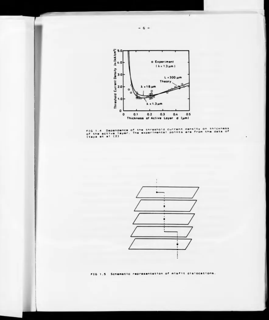
Figure 1.4 shows the dependence of threshold current density on
(2)
thickness d of the active layer , where experimental data
compares reasonably with theoretical curves calculated on the
basis of laser parameters such as loss coefficients.
In ternary heterostructure lasers, an intermediate layer is
sometimes included between the substrate and the heterostructure
wherein the composition is graded so that the active layer and
the adjacent layer have the same lattice constant at the interface.
f i g i a D e p e n d e n c e of tne t h r e s h o l d c u r r e n t Of the a c t i v e layer. The e x p e r i m e n t a l p o i n t * I t a y a et al (2)
d e n s i t y on t h i c k n e s s are f r o m t h e d a t a of
is otherwise large . Experimental observation of highly mis
matched layers grown by LPE has shown that in addition to edge
dislocations in the interface, there are high concentrations of
dislocations (of all types) that penetrate through the grown
structure. The edge dislocations in the interface are parallel
to the growth plane and may not be as serious as the penetrating
or 'inclined' dislocations, which have been observed to have severe
degradation effects on the operation of the lasers. Furthermore,
layers with dislocations that result from lattice mismatch have
been found to have reduced luminescent efficiency in the region
of d i s l o c a t i o n s ^ . Compositional grading, does not however
prevent the formation of dislocations, because lattice mismatch
does occur and this must be accommodated by means of edge dislocations
or the edge component of mixed dislocations. Dislocations that
contribute to strain accommodation are referred to as misfit
dislocations. According to the models of Abrahams et a l ^ ^ and
Matthews et a l ^ \ as the graded layer grows, the lattice parameter
change increases and the strain introduced is accommodated by the
motion, in continuation, of the underlying inclined dislocations.
The result is a dislocation network with portions of a component
or a component of each dislocation parallel to the interfacial
plane. This is illustrated schematically in Figure 1.5 and the
defects are commonly referred to as threading dislocations. If
the mismatch at the growth temperature is too large, a
cross-hatch network of threading dislocation is observed.
8
To improve the quality of devices, a better approach would
be to employ the quaternary alloy I n ^ ^ G a ^ A s w h e r e the
band-gap and lattice constant can be independently adjusted over a
useful range. The growth technology of course becomes a bit more
complicated but the extra degree of freedom permits the fabrication
of strain free heterojunction devices. Because of a differential
thermal expansion coefficient for InP and GalnAsP, a lattice matched
structure at growth temperature to minimize misfit dislocations, may
still result in a residual mismatch at room temperature and most
lasers are designed for CW operation at room temperatures. The
typical lattice parameter mismatch at room temperature is of the
-4
order of 10 or even less. Such closely matched layers call for
more complex growth technology and therefore require assessment on
the uniformity of the epitaxial layers. Thus there is an urgent
requirement for non-destructive methods to ascertain that
compositional and thickness variations are within specified
tolerances and also to evaluate lattice parameter mismatches of
the order of 10 ^ . Also required are methods that would image
any defects in the multilayer structure and at the same time
identify the origin of these defects.
In this thesis, an X-ray double axis diffractometry technique,
which has been successfully employed to meet the abovementioned
objectives for ternary and quaternary III-V multilayer devices
grown by liquid phase epitaxy is described. This work has been
made possible with the active collaboration of Plessey Research
requirements. Use of the SERC facility of the Synchrotron
Radiation Source at Daresbury is also duly acknowledged.
In brief, the technique involves the study of defect type
and distribution in LPE grown double heterostructure lasers and
multilayer structures by plane-wave synchrotron radiation
topography. A double axis diffractometer designed for the
purpose, permits separation of the images from the substrate
(InP) and epilayers (GalnAsP or GalnAs) and hence a precise
location of defects, as well as detailed identification of dis
location type defects. It also enables a very precise plot of
the rocking curves which provides a feast of information including
an assessment of the thickness, compositional variation in the
ternary or quaternary epitaxial layers, and also of the crystalline
perfection of the layers. The technique is capable of mapping
_8
lattice mismatch parameters, of the order of
10
, even thoughof the experimental samples considered, a lowest mismatch of
M « 100 parts per million only could be detected. The experimental
arrangement and the results obtained on several of the specimens
have been presented in detail in Chapters 5-9.
In Chapter 10, a computer simulation of rocking curves from
hétéroépitaxial layers is presented. Initial data from experi
mental rocking curves are used to calculate rocking curves for
the multilayer structure concerned and then compared with the
experimental curves. Input data ere then slightly adjusted about
their initial values until a reasonable fit with experimental
10
layers and their exact compositional variations used in the
simulation can be predicted. Simulation studies have thus been
found to offer a powerful method of detailed interpretation of
experimental rocking curves, and since the experimental arrangement
for plotting rocking curves is non destructive, we virtually have a
powerful, non destructive and an accurate method of assessment of
layer thicknesses and compositional variations. The predicted
thickness of layers by simulation studies have been verified by
other experimental methods in some cases. Simulation studies on a
number of specimens have shown a satisfactory agreement: the
predicted thicknesses have been found to be generally of the same
order as reported by Plessey, and in cases where the data was either
disputed or not available, experimental verification of the thick
ness was made by selective etching. The results in these cases
were found to be in agreement with the thickness predicted from
the X-ray measurements.
The thesis concludes with a general discussion on the various
aspects of the experimental results and on the interpretation of
1 1
References
1. NAHORY, R.E. and POLLACK, M.A., 'Threshold dependence on active
layer thickness in InGaAsP/InP DH lasers', Electron. Lett., JU,
727 (1978).
2. ITAYA, Y., SUEMATSU, Y., KATAYEMA, S., KISHINO, K. and
ARAI, S., 'Low threshold current density (100) GalnAsP/InP
DH lasers for wavelength 1.3 pm', Jpn. J. Appl. Phys., 18,
1795,(1979).
ARAI, S., SUEMATSU, Y. and ITAYA, Y., '1.11 - 1.67 pm (100)
GalnAsP/InP injection lasers prepared by LPE', IEEE J. Quantum
Electron. QE-16, 197 (1980).
NAHORY, R . E ., POLLACK, M.A., BEEBE, E.D. and DeWINTER, J.C.
and DIXON, R.W., 'Continuous operation of 1.0 pm - wavelength
GaAs, Sb /Ai. Ga, As, Sb DH injection lasers at room
1
-x x y1
-y1
-x xtemperature', Appl. Phys. Lett., 28, 19 (1976).
5. BLACK, J.F., SUMMERS, C.J. and SHERMAN, B., 'Spatial variation
of radiative recombination in GaAsP wafer revealed by
photoluminescence image', Appl. Phys. Lett., 1^, 28 (1971)
6
. ABRAHAMS, M.S., WEINSBERG, L.R., BUIOCCHI, C.J. and BLANC, J.,'Dislocation morphology in graded heterojunctions : GaAs^_xP x ',
J. Mater. Science. 223 (1969).
7. MATTHEWS, J.W. and BLAKESLEE, A.E., 'Defects in Epitaxial
2.1. Introduction.
Assessment of the quality of a crystal is vital to both the
crystal grower and the consumer. From the manufacturer's point of
view, the results of the assessment are used to modify the growth
techniques so that any structural imperfections detected in the
assessment are brought to a minimum. The consumer is equally
interested in purer and more perfect crystals so that he can
determine whether the material is capable of being employed in
devices which, otherwise, are known to exhibit performance
characteristics dependent on structural properties of the material
in the device.
The earliest work on the investigation of crystallographic defects
in III-V materials was started in the early 1960's and has continued
since then, with considerable interest. Observation of etch pits,
correlated to edge dislocations in GaAs was made as early as 1959 by
Abrahams and E k s t r o n / ^ .
In this chapter, an attempt is made to review some of the most
common methods to date, of assessment of crystalline perfection, and
the application of these methods to InP based devices is referred
to, wherever possible.
Determination of the elemental composition of quaternary semi
conductor materials used as active layers in double heterostructure
lasers and LEDs is as important as the study of microstructure of
the active layers. Some of the methods that can provide qualitative
and quantitative analysis of microstructural features are also briefly
\
2.2. Assessment of Microstructures.
The methods available for detecting structural imperfections can
be broadly divided into four categories
i) Optical Methods
ii) Transmission Electron Microscopy
iii) Scanning Electron Microscopy
iv) X-ray Topography
2.2.1. Optical Microscopy.
This has been the earliest method of assessment and is still
considered very important in some investigations. The optical
microscope is relatively cheap and easy to operate. The earliest
method of assessment is by etching the material by immersing it in
an etchant which dissolves the material at a rate which is more
rapid at points at which defects intersect the surface of the
crystal. Etch pits are thus produced at the points where the
dislocation lines meet the surface. Sometimes there may be grooves
in the surface resulting from a rapid etch along the line of
intersection of grain boundaries and stacking faults with the
(
2
)surface. This etching technique has been first successfully
used for Germanium using a CP-4 etchant, wherein etch pits were
formed at the dislocations that make up a small angle grain boundary
in Germanium. The spacing between the etch pits, agreed with the
spacing calculated from a measurement of the angle of misorientation
of the grains .
resolution of about 0.5ym. The interpretation of images is however
usually straight-forward. Contrast in the images can be created
by a number of mechanisms based on the reflection, diffraction,
interference and polarization of light waves. Interferometric
methods are extremely good with optical microscopy and are discussed
(3)
in detail by Tolansky . The vertical resolution of the image using
interferometry is improved to much better than 100 0 X . However the
lateral resolution is still poor. This therefore limits the
application of optical microscopy for studying imperfections.
Secondly, only a few materials are transparent to visible light,
hence study of imperfections for an opaque material can only be made
on its surface using optical methods, otherwise thin layers of the
material would have to be successively removed by etching, if the
inside of the material is to be probed.
In some transparent materials, certain impurity precipitates
can be seen by transmission optical microscopy. In certain cases,
these precipitates are arranged along dislocation lines. This
effect has been originally used to observe dislocations and grain
boundaries in transparent ionic crystals like silver chloride by
deliberately introducing impurity precipitates and thereby decorating
(4)
the dislocation . Dislocations in silicon also used to be
s t u d i e d ^ ’^ in this way by decorating with copper and heat
treating the crystal, and by using infrared transmission microscopy,
since silicon is opaque. The more recent methods of electron
microscopy and X-ray topography are much superior.
In as far as the study of imperfections in InGaAsP/InP
supporting tool. Experimental observation of etch pits have
invariably been made in addition to using other methods like X-ray
topography and scanning electron microscopy. Olsen and
Ettenberg^^ compared optical micrographs of top surfaces of
VPE InGaAsP/InP DH lasers and observed that the presence of lattice
mismatch can sometimes be identified by the appearance of a surface
cross-hatched pattern. The cross-hatched pattern is the result of
some perturbations during growth and is caused by the presence of
interfacial misfit dislocations. InGaAsP/InP alloys seem to accommodate
higher amounts of elastic strain without forming misfit dislocations
(probably due to smaller elastic constants of InP compared to GaAs).
Hence an absence of misfit dislocation network would not necessarily
/ Q\
mean perfect lattice match. Nakajima et alv ' observed that for an
LPE grown InGaAsP/InP heterostructure wafers, the dislocation-free
regions determined by the etch pit observation of InP alone was
found to correspond to regions where dislocations form in neither
InP nor In Ga, As, P (as observed by X-ray transmission topograph x
1
—x1
—y yfor the InGaAsP/InP wafers) and concluded that dislocations are not
introduced into Inx<'a i_xA s l-y^>y w^ erewer dislocations do not form
in InP. Since some of the dislocations in the substrate necessarily
propagate through the epilayer and reach the surface, it is significant
that the dislocation free region of InP is determined by etch pit
observation.
A more general and detailed discussion on optical microscopy is
■ads by R i c h a r d s o n S h i r a f u j i et a l ^ ° ^ have analysed photo
micrographs of as-grown, as well as chemically etched surfaces of
16
the surface for samples whose (Aa/a) exceeds 0.3%. The results are
in general agreement with those of Feng et a l ^ ^ (± 0.2%) but
(12)
deviates from those of Oe et al (± 0.5%). This shows that the
lattice mismatch limits needed to give acceptable surface morphology
is indeed a function of the thickness of the epilayer grown. Shirafuji
used a thickness of 3-5pm for the epilayer, compared to 3-4pm used by
Feng and only 0.4pm used by O e .
. (13)
Hsieh used the Nomarski and Mirau techniques of optical
interference-contrast microscopy to examine surface morphology of
GaAs layers grown by LPE under different conditions to observe
discrete features like pits and hillocks with the Nomarski technique
and assess surface flatness from the fringe patterns produced by
the Mirau technique. Layers with a smooth and flat surface, as
thick as 26pm could be grown by the super cooling technique. Step
cooling also gives identical, if not slightly better results, but
for thin layers of about 0.5pm thickness.
2.2.2. Transmission Electron Microscopy.
Imaging methods by TEM are superior to optical methods in the
sense that since electrons can penetrate into materials more easily
than visible light, a three dimensional microstructure of an opaque
material may be observed without etching in succession. The depth
of penetration depends on the material and the electron energy and
specimen thicknesses of roughly about 0.3pm at 100 KeV and about
lpm at 1 MeV, depending on the material, can be analyzed. Using a
high electron energy 100 KeV - 1 MeV makes the wavelength very short
16
the surface for samples whose (Aa/a) exceeds 0.3%. The results are
in general agreement with those of Feng et al^ ^ (± 0.2%) but
(12)
deviates from those of Oe et al (± 0.5%). This shows that the
lattice mismatch limits needed to give acceptable surface morphology
is indeed a function of the thickness of the epilayer grown. Shirafuji
used a thickness of 3-5pm for the epilayer, compared to 3-4pm used by
Feng and only 0.4pm used by O e .
(131
Hsieh used the Nomarski and Mirau techniques of optical
interference-contrast microscopy to examine surface morphology of
GaAs layers grown by LPE under different conditions to observe
discrete features like pits and hillocks with the Nomarski technique
and assess surface flatness from the fringe patterns produced by
the Mirau technique. Layers with a smooth and flat surface, as
thick as 26pm could be grown by the super cooling technique. Step
cooling also gives identical, if not slightly better results, but
for thin layers of about 0.5pm thickness.
2.2.2. Transmission Electron Microscopy.
Imaging methods by TEM are superior to optical methods in the
sense that since electrons can penetrate into materials more easily
than visible light, a three dimensional microstructure of an opaque
material may be observed without etching in succession. The depth
of penetration depends on the material and the electron energy and
specimen thicknesses of roughly about 0.3pm at 100 KeV and about
lpm at 1 MeV, depending on the material, can be analyzed. Using a
high electron energy 100 KeV - 1 MeV makes the wavelength very short
Electron microscopy basically involves scattering processes
that take place when the electron beam travels through the specimen.
The scattering processes may be divided into two categories: elastic
and inelastic. Elastic scattering involves interaction of the
electrons and the effective field potential of the nuclei, with no
energy losses. Inelastic scattering involves interaction of electrons
with electrons in the specimen and results in energy losses.
Diffraction patterns produced by elastic scattering form the basis
for studying imperfections in materials. Inelastic scattering, however,
also produces informative diffraction effects i.e., Kikuchi patterns,
but they are more readily used to analyse spectroscopic data resulting
from characteristic energy losses and emissions due to absorption
effects of the inelastic scattering. These include Auger Spectroscopy
and X-ray fluorescence.
A detailed account of the electron optics and electron microscopy
are available in many standard t e x t s ^ ^ ’ while a more concise
• = „ ,,(17)
account is given in Bowen and Hall
The advantages of high resolution in a TEM will have to be
weighed against the high cost of the instrument. Economic utilization
means that most TEM work is concentrated on specimens known to have
high density of dislocations and very rarely on highly perfect
crystals like Si. Secondly,the accessible thickness of the specimen
is roughly up to 1pm and if one utilizes the high resolving power of
the TEM to record a micrograph at a high magnification, the information
on the micrograph would actually be resulting from a very tiny volume
18
about lum thick. Transmission electron microscopy essentially
operates in the transmission mode while optical microscopy can also
be in the reflected mode. A TEM can very easily produce the micro
graph and the electron diffraction pattern for the same area of the
specimen. Essentially the formation of micrographs and diffraction
patterns in a TEM can be explained as follows. Figure 2.1 shows a
simple sketch of a vertical cross-section of a TEM, which consists
of an electron gun to inject an electron beam and a number of
electron lenses, which act in much the same way as optical lenses
for visible light, a fluorescent screen to observe the diffraction
pattern and a photographic plate to record the image.
E lK tro n
gun
Viewing p o rt
F lu o re s c e n t screen which con be tilte d out of the way for p ho tograp h y
To vacu um p u m p s
19
1
» I. ISpocimen object points
diffracted ( B rag g reflected ) beams principal pione of the objective lens Bock focal oione of the objective lens diffraction p a tte rn : rays of "eauol inclin ation " ore brought together m the spots m d ic o te d O bjective a p e rtu re allows only chosen beams through
First intermediate image
Three image points corresponding to 0 , , 0 * . O3
FIG 2.2 F o r m a t i o n of a m i c r o g r a p h a nd d i f f r a c t i o n p a t t e r n in a TEM.
Figure 2.2 gives an idea of formation of the micrograph and
diffraction pattern of a specimen. A thin specimen placed inside
the objective lens and above the principal plane of the lens,
diffracts the incoming electron beam passing through it. These
diffracted beams are further deflected by the lens in such a way
that rays of equal inclination to the vertical axis at the principal
plane of the lens intersect at the focal plane to form the diffraction
pattern. Rays from the same object point, however, intersect in the
conjugate plane to produce a real image. An intermediate lens is
used to alter the focal length of the objective lens and can thereby
focus either the diffraction pattern or the image on a viewing screen
Application of this method to InGaAsP/InP layers has not been
widely reported, the one drawback being to etch the specimen to
up to lum thick for defect analysis.
(18)
Ueda et al' ' report studying the nature of dark defects in
InGaAsP/InP LEDs grown by LPE, by transmission electron microscopy
and other related methods. Electron micrographs of a part of the
active region obtained by (220), (220), (400) and (040) reflections
were shown to exhibit two sets of misfit dislocations lying in
two equivalent directions of (110) and (110). The five types of
dark defects observed in the experiment, namely a) cross hatched
dark line defect, b) regular tetragonal DLD, c) regularly distributed
dark spot defects, d) dark band defects and e) a DSD whose
circumference is bright, were considered to originate from i) misfit
dislocations ii) stacking faults between the epilayer and substrate
interface iii) precipitates iv) mechanical damages and
v) crystallographically anomalous region due to the penetration
of the p-electrode in the LED structure, respectively. From the
study of the contrasts in the transmission electron micrographs
showing misfit dislocations under four different reflections, the
dislocation dipoles were observed to be associated with Burgers
vectors of the type a
/2
(101
) and a/2
(0 11
) as evidenced in a morerecent paper of the same author . Olsen
^2
^ has observed from twocross-sectional TEM micrographs of InGaAsP/InP DH lasers grown by
iPI that conditions during a praheat process prior to growth of
High resolution transmission electron microscopy has made it
possible to study interfaces using lattice imaging. In the case of
epitaxial semiconductor multilayer structures like InGaAsP/InP which
contain similar materials in its layers, it is sometimes difficult to
get a good contrast, between the layers, from the axial high resolution
TEM images of these structures. This lack of contrast sometimes makes
it difficult to observe atomic height steps at the interface.
.
(
2 1)
Hetherington et al have devised a "near axial lattice imaging"
technique to overcome the lack of contrast between layers of similar
materials and have applied this technique to GaAlAs/GaAs multilayers
to study interfacial steps and the roughness of each interface as
well as the determination of the widths of each layer to an accuracy
of about lX. High resolution electron microscopy has been widely
. . . (
22
)applied to silicon. Smith et al have observed changes in the
morphology of silicon-on-sapphire films that were Si implanted and
electron-beam annealed. A comparison of a high resolution
lattice image of an as - grown Si-on-sapphire with the one
after annealing the sample has shown that defects like stacking
faults and micro-twins are removed. Some of the recent studies of
(23)
semiconductor interfaces made by Sinclair' ' using HREM, include
correlation of the fine structure of interfaces with the materials
processing and the physical properties of the materials.
In a multilayer structure, high resolution TEM is thus extremely
useful for seeing sharpness of interface, dislocations generated from
2.2.3. Scanning Electron Microscopy
The scanning electron microscope is a much more versatile
instrument than the TEM. It can in fact provide a whole range
of techniques. Basically, in an SEM, a fine high energy beam of
electrons from an electron gun are focussed by magnetic lenses
so as to produce a point electron source (as small as 5oX in
diameter) on a specimen surface. The beam is additionally guided
by an objective lens containing scanning coils so that it scans
line by line a TV type raster, over the specimen surface. By the
impact of the electron beam on the specimen surface, other forms
of energy are dissipated from the specimen (thus giving rise to
various modes of operation of the SEM). Any of these can be collected
and converted into an electrical signal and amplified. A CRO, scanned
in synchronism with the electron beam scanning, would convert this
electrical signal into a suitable video display. Any variation in
the strength of the signal scattered from a specimen point would
result in a variation in the intensity at a corresponding point
on the CRO display. These give rise to contrasts in the SEM
micrographs. The magnification of the micrograph is given by the
ratio of the side lengths of the area scanned on the CRO to the
side length of the area scanned on the specimen and is in general
variable from 20X to about 100000X. Figure 2.3 gives a schematic


![FIG 2.3 S c h e m a t i c d i a g r a m of a s c a n n i n g e l e c t r o n m i c r o s c o p e , [a f t e r B o w e n a nd Hall (17)]](https://thumb-us.123doks.com/thumbv2/123dok_us/9883559.489584/48.1026.40.990.24.1060/fig-s-of-r-o-b-nd-hall.webp)