1
Remotely controlled isomer selective molecular
switching
Verena Schendel
1*, Bogdana Borca
1, Ivan Pentegov
1, Tomasz Michnowicz
1, Ulrike Kraft
1,
Hagen Klauk
1, Peter Wahl
1, 2, Uta Schlickum
1and Klaus Kern
1, 31 Max Planck Institute for Solid State Research, Stuttgart, Germany
2SUPA, School of Physics and Astronomy, University of St. Andrews, Scotland, United Kingdom 3Ecole Polytechnique Fédérale de Lausanne, Switzerland
Abstract
Nonlocal addressing - the “remote control”- of molecular switches promises more efficient
processing for information technology, where fast speed of switching is essential. The surface state of the (111) facets of noble metals, a confined two-dimensional electron gas, provides a medium that enables transport of signals over large distances and hence can be used to address an entire ensemble of molecules simultaneously with a single stimulus. In this study we employ this
characteristic to trigger a conformational switch in anthradithiophene (ADT) molecules by injection of hot carriers from a scanning tunneling microscope (STM) tip into the surface state of Cu(111). The carriers propagate laterally and trigger the switch in molecules at distances as far as 100 nm from the tip location. The switching process is shown to be long-ranged, fully reversible and isomer selective, discriminating between cis and trans diastereomers, enabling maximum control.
2
Future electronic devices based on functionalities of single molecules are one route that is envisioned to revolutionize current technology 1. Molecular switches represent such functional
components that can be reversibly and repeatedly interconverted between two or more stable states. Switching of individual molecules2–9 is by now well established, however for rapid information
processing, parallel addressing, which is effective over large distances is desirable. One way to meet these requirements is to use surface state carriers present within the first few atomic layers of the (111) faces of noble metals which have a free electron-like character10–13. Hot carriers that are
injected from an STM tip can travel laterally in the surface state to the molecule and induce
reactions in a spatially extended area around the tip location. In this context, it has been shown that molecules can be dissociated in a certain radius around the tip, which however is an irreversible process14–17. For actual devices reversible processes are much more relevant. Therefore, we employ
molecular switches which are “remotely” toggled by means of surface state carriers.
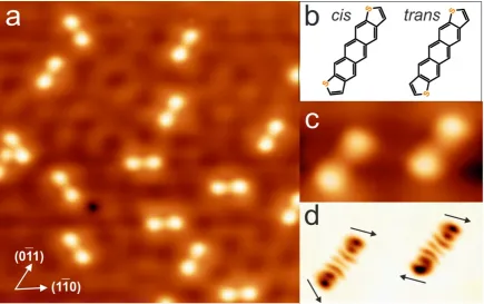
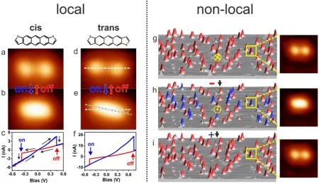
As a molecular switch, we use the anthradithiophene (ADT), which is a structural analog of pentace. Individual ADT molecules adsorb on Cu(111) in a dumbbell-like appearance aligned along the close-packed directions (Fig. 1a). The source material contains an equal mixture of two diastereomers, cis and trans (Fig. 1b), which cannot be discriminated when imaged in constant current mode with a metallic tip (Fig. 1c). Using a functionalized ADT tip their orbital structure can be visualized enabling the distinction between thediastereomers18,19 (Fig. 1d). Local switching is conducted by positioning
the tip apex on top of an individual molecule (Fig. 2a, b). Sweeping the applied bias voltage from positive to negative and back reveals a hysteretic current-voltage (I-V) characteristics (Fig. 2c). When ramping the voltage V from positive to negative (red curve in Fig. 2c), an abrupt increase in the current at negative bias indicates a change to a higher conductivity accompanied by a change in the topographic appearance of the molecule from a dumbbell-like to a rod-like structure (Fig. 2a, b). When ramping the voltage in the opposite direction (blue curve in Fig. 2c) the initial conformation is restored at a positive bias, apparent by a sudden drop of the current. In the following, the
3
“on” state, whereas the one with the lower conductance to as the “off” state. A similar switching behavior is observed for the trans isomer (Fig. 2d, e), which however undergoes an additional rotation upon switching and for which the switching occurs at slightly higher voltages (Fig. 2f) compared to the cis molecule (Fig. 2c). The two isomers constitute voltage-controlled conductance switches whose switching characteristics differ solely in their threshold energies.
The underlying switching mechanism can be attributed to a change of the molecule-substrate interaction accompanied with a conformational change of the molecule, which has been experimentally demonstrated for the ADT molecule9 and theoretically predicted for benzene
derivatives20. The ADT molecule possesses a bistable behavior between a strongly and a weakly
bound state on a metal surface. A strong interaction arises at a small molecule-substrate separation leading to a substantial hybridization, whereas a weaker interaction is caused by an increased separation between molecule and substrate and the hybridization is reduced. In the former case the molecular orbitals are broadened and shifted in energy, while in the latter they remain mostly unaffected.
Constant height scans acquired at small bias voltages with a functionalized tip reveal that the orbital structures close to the Fermi energy (EF) resemble the LUMO (lowest unoccupied molecular orbital)
in the “off” state and the HOMO (highest occupied molecular orbital) in the “on” state (see Supporting Information (SI)). As shown by Borca et al.9 in the “off” state the molecular orbitals
strongly hybridize with the Cu substrate, leading to a partial population of the LUMO accompanied by a shift of the LUMO to the Fermi energy. Conversely, in the “on” state we image the HOMO closer to EF, which corresponds more to the electronic configuration of the molecule in the gas phase,
indicating a much weaker interaction.
4
molecule is switched back to its pristine configuration by injection of charge carriers at a voltage of about 0.4 V.
The necessity for charge carriers of different polarities to initialize the switching and back-switching, respectively, gives rise to the directionality of the process.
The non-local switching process is induced by hot carriers injected from the STM tip into the Cu substrate. Applying a negative voltage pulse (pulse position indicated by the yellow cross in Fig. 2g) activates switching of about 50 % of the molecules to their “on” state within an area of 80 nm x 80 nm around the pulse position (Fig. 2h, blue coded molecules). Applying the same pulse with opposite voltage polarity switches all molecules back to the “off” state (Fig. 2i). These characteristics,
switching from “off” to “on” by a negative voltage pulse and switching back from “on” to “off” by a positive pulse, demonstrate a direct analogy to the local switching process. Addressing the molecule locally and non-locally results in the same “off” and “on” state, respectively (compare Fig. 2a, b with insets in Fig. 2g, h).
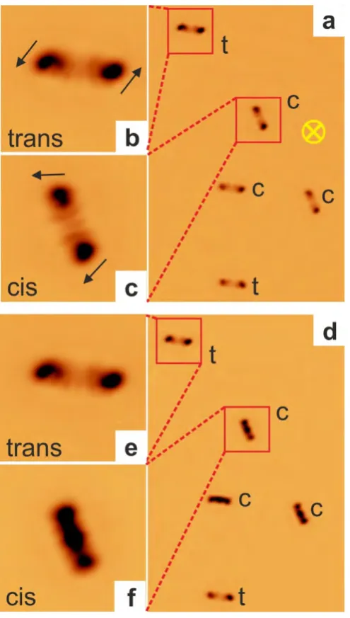
From isomer-resolving images obtained with a functionalized tip before (Fig. 3a-c) and after (Fig. 3d-f) applying a voltage pulse, we can deduce that the non-local switching process only addresses cis isomers, whereas trans isomers remain in their initial configuration. This is in contrast to the locally initiated switching process where both isomers were switchable. Therefore, the non-local process is found to be isomer selective and explains why only about 50 % of the molecules can be addressed (Fig. 2h).
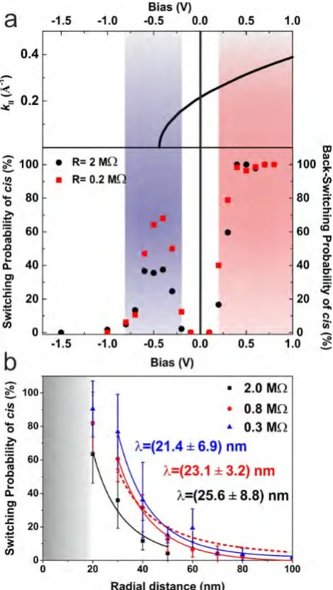
Exploring the non-local switching process for different negative bias values within an area of 80 nm x 80 nm (lower panel of Fig. 4a) reveals that the switching probability from the “off” to the “on” state increases steadily from -0.2 V to -0.5 V and then almost vanishes at -1 V. From this we can conclude that to trigger the switching process, a threshold energy of the charge carriers is required.
5
means of an electric field effect can be ruled out, in which case the switching probability would be expected to increase with increasing bias instead of the observed decrease for bias voltages beyond -0.5 V. The voltage dependence for positive polarities (Fig. 4a) shows a drastic increase of the probability for remote switching from the “on” to the “off” state exceeding a bias voltage of 0.35 V. Beyond this threshold voltage, the probability to switch the molecules back into their initial
conformation is about 100 %, indicating a highly efficient “back”-switching process.
All these characteristics strongly suggest that the remote switching is mediated by the surface state of the Cu(111) surface. The surface state has an onset energy of -0.44 eV10,12, which coincides with
the voltage at which the maximum switching probability occurs at negative voltages (Fig. 4a, upper panel). Holes propagating in the surface state can only possess energies up to the onset energy. Therefore, switching is only enabled if the threshold voltage for the switching process lies within the energy range of the surface state. Since slightly higher energies are required for the trans species, which lie beyond the onset of the surface state (Fig. 2 f), the switching process cannot be induced by charge carriers propagated through the surface state. To trigger the switching/back-switching process via the surface state, the energy window where the surface state is present must coincide with the excitation energy required to switch the molecule.
The decrease in the switching probability at negative bias voltages beyond -0.5 V is due to increased tunneling into the bulk states. The lower edge of the directional band gap in which the surface state exists is at -0.7eV12. As charge carriers with all energies between the applied voltage and the Fermi
energy contribute to the current, an increased tunneling of charge carriers from the tip into the bulk state at more negative bias voltages leads to a reduced switching probability.
Further evidence for the mechanism involving the surface state is provided by experiments
performed near monatomic steps, which constitute a potential barrier for the surface state electrons
23, but would not effect, e.g., the distance dependence expected for a mechanism due to electric
6
the same terrace on which the pulse has been applied than on an adjacent terrace, where the switching probability is significantly reduced (see SI). Hence, in the case of surface state mediated switching the hot carriers that are injected from the tip into the substrate are “transported” by the surface state carriers to the molecules where they interact with the molecule thereby inducing the switch. In contrast, for local excitations the charge carriers from the tip directly trigger the molecule. Most importantly, the switching characteristics that have been explored locally remain the same for the non-local excitation - only the way of addressing differs. If at all, the surface state plays only a negligible role for the local switching, as when triggering a molecule locally the surrounding molecules are not affected.
To extract quantitative information about the spatial dependence of the switching probability, we have studied the process at negative bias polarity at a voltage of -0.4 V for three different currents as a function of the radial distance with a bin size of 10 nm. The distance dependence is
characterized by a saturation regime in the immediate vicinity of the pulse position, where all cis isomers are switched (Fig. 4b, grey shaded area). For larger distances the probability decays in a characteristic manner, which is governed by a geometric 1/r behavior as well as by the coherence length λ of the charge carriers. The 1/r dependence is distinctive for the decay of quasiparticles in a two-dimensional gas, in contrast to a bulk dominated process where the decay is governed by a 1/r2
behavior. The best fit is obtained for a 1/r dependence and treating the coherence length as a fit parameter yields about λ=23 nm at -0.4 V. In addition, the switching probability is reduced for a lower current (Fig. 4b) and shorter injection times of the hot carriers (see SI).
The efficiency for surface state mediated switching from “on” to “off” and vice-versa is not identical. This asymmetry arises due the different coherence lengths λ for holes and electrons within the surface state. The coherence length sets the distance over which the charge carriers propagate without scattering while retaining their energy. The coherence length is directly related to the lifetime of the charge carriers τ and their group velocity vg. It has been shown from calculations that
7
voltages of 0.3 V and -0.3 V, the lifetimes amount to 113 fs and 62 fs 25 with corresponding group
velocities of 0.83·106 m/s and 0.36·106 m/s, resulting in coherence lengths λ of about 93 nm and 22
nm, respectively. Hence surface state-mediated switching at positive polarity is substantially more efficient compared to the process at negative polarity.
In conclusion, we have demonstrated a surface state-mediated switching process that is effective over distances on the order of 100 nm. The local switching characteristics of the single molecules directly translate into the non-local switching process. The interplay of the molecule’s electronic states and the surface state of Cu(111) enables remote-control, reversibility, directionality and isomer selectivity at the same time. These features allow a precise control of the system and provide a new pathway towards rapid write/delete processes for future device elements.
Methods
Sample preparation
Experiments were conducted in a home-built low-temperature scanning tunneling microscope operating in ultra-high vacuum and at a base temperature of about 7 K. The Cu(111) single crystal was cleaned by repeated cycles of Ar+ sputtering and annealing up to 800 K. ADT molecules were
thermally evaporated using a quartz crucible at a temperature of 505-510 K for 15 -18 minutes with the Cu substrate cooled down to 210 K. The crystalline powder was used as obtained from Sigma Aldrich. The sample was transferred in situ into the STM chamber.
8
I-V measurements acquired on top of the molecule were recorded as the sample voltage was ramped between 0.6 V and -0.6 V and back for the cis and 0.7 V and -0.6 V within 10 s for the trans molecule with a setpoint of 100 mV and 100 pA. Bias voltages are applied to the sample, with the tip at virtual ground.
Supporting Information
Supporting Information available: Orbital structure of the non-switched and switched state and switching mechanism, ADT adsorption on Cu(111), Switching at step edges, Influence of pulse length and current on probability of remote switching, efficiency of remote back-switching process. This material is available free of charge via the Internet at http://pubs.acs.org.
Author information:
*Email: [email protected]
Acknowledgements
We thank A. Arnau and M. Ternes for discussions on the switching mechanism. We acknowledge funding by the Emmy-Noether-Program of the Deutsche Forschungsgemeinschaft, the SFB 767, and the Baden-Württemberg Stiftung.
Notes
9
References
(1) Lörtscher, E. Nat. Nanotechnol.2013, 8, 381–384. (2) Liljeroth, P.; Repp, J.; Meyer, G. Science2007, 317, 1203–1206.
(3) Wu, S. W.; Ogawa, N.; Nazin, G. V.; Ho, W. J. Phys. Chem. C2008, 112, 5241–5244. (4) Wu, S. W.; Ho, W. Phys. Rev. B2010, 82, 085444.
(5) Swart, I.; Sonnleitner, T.; Repp, J. Nano Lett.2011, 11, 1580–1584.
(6) Weigelt, S.; Busse, C.; Petersen, L.; Rauls, E.; Hammer, B.; Gothelf, K. V; Besenbacher, F.; Linderoth, T. R. Nat. Mater.2006, 5, 112–117.
(7) Moresco, F.; Meyer, G.; Tang, H.; Joachim, C. J. Elecrtron Spectrosc. Relat. Phenom.2003, 129, 149–155.
(8) Mohn, F.; Repp, J.; Gross, L.; Meyer, G.; Dyer, M. S.; Persson, M. Phys. Rev. Lett.2010, 105, 266102.
(9) Borca, B.; Schendel, V.; Petuya, R.; Pentegov, I.; Michnowicz, T.; Kraft, U.; Klauk, H.; Arnau, A.; Wahl, P.; Schlickum, U.; Kern, K. ACS Nano2015, DOI:10.1021/ascnano.5b06000.
(10) Crommie, M. F.; Lutz, C. P.; Eigler, D. M. Nature1993, 363, 524–527. (11) Manoharan, H. C.; Lutz, C. P.; Eigler, D. M. Nature. 2000, pp 512–515. (12) Hörmandinger, G. Phys. Rev. B1994, 49, 13897–13905.
(13) MacLeod, J. M.; Lipton-Duffin, J.; Fu, C.; Rosei, F. ACS Nano2009, 3, 3347–3351. (14) Maksymovych, P.; Dougherty, D.; Zhu, X.-Y.; Yates, J. Phys. Rev. Lett.2007, 99, 016101. (15) Chen, L.; Li, H.; Wee, A. T. S. ACS Nano2009, 3, 3684–3690.
(16) Ladenthin, J. N.; Grill, L.; Gawinkowski, S.; Liu, S.; Waluk, J.; Kumagai, T. ACS Nano2015, 9, 7287–7295.
(17) Sloan, P. A.; Sakulsermsuk, S.; Palmer, R. E. Phys. Rev. Lett.2010, 105, 048301.
(18) Gross, L.; Moll, N.; Mohn, F.; Curioni, A.; Meyer, G.; Hanke, F.; Persson, M. Phys. Rev. Lett.
2011, 107, 086101.
(19) Repp, J.; Meyer, G.; Stojković, S. M.; Gourdon, A.; Joachim, C. Phys. Rev. Lett.2005, 94, 026803.
10 (22) Gadzuk, J. W. Phys. Rev. Lett.1996, 76, 4234–4237.
(23) Avouris, P.; Lyo, I.-W.; Molinàs-Mata, P. Chem. Phys. Lett.1995, 240, 423–428.
(24) Kliewer, J.; Berndt, R.; Chulkov, E. V.; Silkin, V. M.; Echenique, P. M.; Crampin, S. Science2000, 288, 1399–1402.
(25) Echenique, P. M.; Osma, J.; Machado, M.; Silkin, V. M.; Chulkov, E. V.; Pitarke, J. M. Prog. Surf. Sci.2001, 67, 271–283.
(26) Echenique, P. M.; Berndt, R.; Chulkov, E. V.; Fauster, T.; Goldmann, A.; Höfer, U. Surf. Sci. Rep.
11
12
Figure 2: Local and Non-local switching: a-f, local switching: a, b, d, e, Constant current scans (3 nm x 2.2 nm, 0.1 nA, 0.1 V) of the non-switched (a, d) and switched (b, e) structures of the cis (a,b) and trans (d, e) isomers. c, f, I-V curves acquired on the cis (c) and trans (f) isomers. Switching from the “off” to the “on” state (blue arrow) occurs at negative bias concomitant with a change from a lower to a higher conductivity. Switching from “on” to “off” (red arrow) is triggered at positive voltages, indicated by an abrupt change from a high conducting to a low conducting state (at same tip-sample distance). g-i, non-local switching: g, STM constant current image (80 nm x 80 nm, 0.1 nA and 0.1 V) showing all molecules in the “off” state. Applying a pulse (yellow cross) of -0.4 V for 16 sec (I= 2.2 μA) directly into the bare copper substrate enables switching of the molecules to the “on” state. h,
13
14
Figure 4: (a) Bias dependence of the switching probability. (a) Upper panel: The dispersion of the surface state of Cu(111) is shown for comparison, with an onset energy of −0.4 V and an effective mass m* = 0.4me. Lower panel: Probability of switching and back-switching the cis isomers remotely as a function of bias voltage, within an area of 80 nm × 80 nm. Data have been recorded with two different tunnel resistances, R = 2 and 0.2 MΩ. The switching process is initiated at negative bias (blue shaded) and the back-switching at positive bias (red shaded). (b), radial decay of the switching probability measured at a voltage of -0.4 V and different currents. The tail of the decay curve was fitted by an exponential function 1/r exp(-r/λ), where r denotes the radial distance and λ the decay length. The region in close proximity to the location where the pulse was applied was ignored in the fit due to saturation. Red dotted line represents a decay governed by a 1/r2 dependence, which would be expected for a bulk dependent