ISSN Print: 2162-531X
DOI: 10.4236/ampc.2019.94007 Apr. 26, 2019 71 Advances in Materials Physics and Chemistry
Effect of Organic Dopants in
Dimetallophthalocyanine Thin Films:
Application to Optoelectronic Devices
María Elena Sánchez-Vergara
*, Santiago Osorio-Lefler, Pablo Osorio-Lefler,
José Ramón Álvarez-Bada
Universidad Anáhuac México, Avenida Universidad Anáhuac 46, Col. Lomas Anáhuac, Huixquilucan, Estado de México, México
Abstract
Semiconductor films of organic, doped dimetallophthalocyanine M2Pcs (M =
Li, Na) on different substrates were prepared by synthesis and vacuum eva-poration. Tetrathiafulvalene (TTF) and tetracyanoquinodimethane (TCNQ) were used as dopants and the structure and morphology of the semiconduc-tor films were studied using IR spectroscopy, X-ray diffraction (XRD), Scan-ning Electron Microscopy (SEM) and Energy Dispersive X-Ray Spectroscopy (EDS). The absorption spectra recorded in the ultraviolet-visible region for the deposited films showed the Q and Soret bands related to the electronic
π-π* transitions in M2Pc molecules. Optical characterization of the films
in-dicates electronic transitions characteristic of amorphous thin films with opt-ical bandgaps between 1.2 and 2.4 eV. Finally, glass/ITO/doped M2Pc/Ag
thin-film devices were produced and their electrical behavior was evaluated by using the four-tip collinear method. The devices manufactured from Na2Pc
have a small rectifying effect, regardless of the organic dopant used, while the device manufactured from Li2Pc-TCNQ presents ohmic-like behavior at low
voltages, with an insulating threshold around 19 V. Parameters such as the hole mobility (µ), the concentration of thermally-generated holes (p0), the
concentration of traps per unit of energy (P0) and the total trap concentration
(Nt(e)) were also determined for the Li2Pc-TTF device.
Keywords
Organic Semiconductors, Thin Films, Optical Properties, Electrical Properties, Optoelectronic Devices
1. Introduction
The field of optoelectronics has been recently evolving towards the substitution
How to cite this paper: Sánchez-Vergara, M.E., Osorio-Lefler, S., Osorio-Lefler, P. and Álvarez-Bada, J.R. (2019) Effect of Organic Dopants in Dimetallophthalocya-nine Thin Films: Application to
Optoelec-tronic Devices. Advances in Materials
Physics and Chemistry, 9, 71-88. https://doi.org/10.4236/ampc.2019.94007
Received: January 18, 2019 Accepted: April 23, 2019 Published: April 26, 2019
Copyright © 2019 by author(s) and Scientific Research Publishing Inc. This work is licensed under the Creative Commons Attribution International License (CC BY 4.0).
http://creativecommons.org/licenses/by/4.0/
DOI: 10.4236/ampc.2019.94007 72 Advances in Materials Physics and Chemistry
of inorganic semiconductors for organic ones. The use of organic chemistry gives us new ways of modifying materials’ functional properties, opening several possibilities for inexpensive device manufacturing [1]. The introduction of these materials permits the development of new, cheaper, optoelectronic devices, such as organic diodes [2], organic light-emitting field-effect transistors [3] and or-ganic light-emitting diodes [4]. Among the organic materials employed, phtha-locyanines (Pcs) stand out, as they become reasonably good semiconductors when doped [5]. The central cavity of macrocycle is to be capable of accommo-dating different elemental ions. A Pc containing one or two metal ions is called a metallophthalocyanine (MPc). A problem with the use of organic materials as sensitizers for semiconductors is the low efficiency for conversion of incident radiation to electron flow. This can be attributed to the low conversion efficiency of excitons to form separate electron-hole pairs and to the low mobility and rapid carrier trapping in organic semiconductors [1]. MPcs show a tendency toward aggregation and polymerization in the solid state. This could lead to a better orbital overlap between molecules and improve charge carrier photoge-neration and conduction. MPcs are also thermally and chemically stable in most instances and are endowed with optical and electrical properties that are suitable for optoelectronics applications [6]. Substantial research in this field has been done with the purpose of developing p-type, MPcs-based semiconductors, such as ZnPc [7], CoPc [8] [9], FePc and NiPc [9]. On the other hand, relatively little work has been reported regarding those MPcs, including alkali metals. There are publications about LiPc, but they mainly focus on thin-film preparation and morphology [10][11]. Few reports have been published regarding their optoe-lectronic properties [12]. Additionally, most of the MPcs occur in at least three different crystalline structures, the metastable α, the β and the χ polymorphs
[11]. LiPc is distinct from other MPcs in that it shows a peculiar polymorphism in powders and thin films. LiPc occurs in the χ and α polymorphs, depending on the synthesis route used for powder growth or on the substrate temperature used in thin-film deposition [11]. The χ structure of LiPc is tetragonal, while α struc-ture shows a monoclinic unit cell, both strucstruc-tures being responsible for LiPc’s optoelectronic properties. Important modifications of the optical spectra in the Q-band domain have been reported as a consequence of the χ → α phase change
[11]. For LiPc, the Q-band can be observed in the visible region and is assigned to the π-π* electronic transition, so it is very important to take into account the crystalline structure of the molecule and the changes it goes through during thin-film manufacture. One of the objectives of this work was to develop four devices through the synthesis and analysis of the structure and to evaluate the optoelectronic properties of doped alkali M2Pcs, using disodium and dilithium
DOI: 10.4236/ampc.2019.94007 73 Advances in Materials Physics and Chemistry
in the material [13]. M2Pc (M = Li, Na) behavior as p-type or n-type
semicon-ductor in optoelectronic devices is also evaluated in this work, as is well known that some Pcs can behave as both semiconductor types. To accomplish these ob-jectives, tetrathiafulvalene (TTF) and tetracyanoquinodimethane (TCNQ) were used as dopants and the doped semiconductors were deposited as thin films, which were structurally characterized and whose optoelectronic properties were evaluated. TTF and TCNQ were chosen as dopants because they are flat mole-cules that can form molecular blocks. They also have π orbitals located in such a way that permits interaction with the M2Pcs and provides the capability to give
(TTF) or accept (TCNQ) π electrons with a low energetic cost, in such a way that the resulting energy bands can be partially occupied. Valence electrons in TTF and TCNQ are located above and below the medium plane of the molecule in delocalized π orbitals. It is worth mentioning that this type of flat molecules has a preferential stacking direction, which means that materials derived from them have an anisotropic conductivity and can be described as “quasi one-dimensional”, the conductivity being much larger in the stacking direction than in the other directions within the material.
2. Experimental Methods
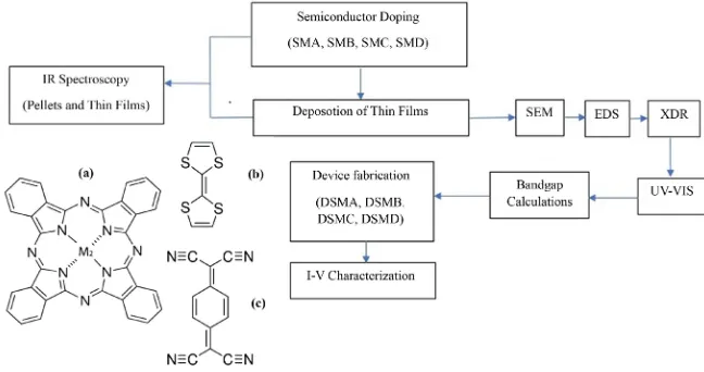
This study was carried out according to the methodology shown in the diagram of Figure 1. First, M2Pc (M = Na, Li) was doped with TTF and TCNQ through a
[image:3.595.210.534.522.693.2]simple reflux reaction. Subsequently, the doped semiconductors were evaporated in high vacuum in order to produce thin films from each material. Vacuum evaporation is a physical method that involves vapor production from low-pressure sublimation of the semiconductor source in powder form. The vapor thus gen-erated is transported from the source to the substrate surface at room tempera-ture, where it condenses and forms a solid film on the substrate’s surface [14]. Thin-film production is of particular interest, as microelectronic solid-state de-vices are generally formed by thin-film semiconductor structures.
Figure 1. Diagram of experimental method and structures of (a) M2Pc (M = Li, Na), (b)
DOI: 10.4236/ampc.2019.94007 74 Advances in Materials Physics and Chemistry
TTF (tetrathiafulvalene: C6H4S4), TCNQ (7,7,8,8-tetracyanoquinodimethane:
C12H4N4), Li2Pc (dilithium phthalocyanine: C32H16Li2N8) and Na2Pc (disodium
phthalocyanine: C32H16N8Na2) were obtained from Sigma-Aldrich and required
no further purification (see Figure 1). A series of four semiconductor materials (SM) were doped by a simple reaction between M2Pcs (M = Li, Na) and TTF and
TCNQ. SMA: 125 mg (0.24 mmol) of Li2Pc or SMB: 250 mg (0.45 mmol) of
Na2Pc are added to 182.5 mg (0.89 mmol) and 344 mg (1.68 mmol) of TTF,
re-spectively. SMC: 125 mg (0.24 mmol) of Li2Pc or SMD: 250 mg (0.45 mmol) of
Na2Pc are added to 96 mg (0.47 mmol) and 182 mg (0.89 mmol) of TCNQ,
re-spectively, and dissolved in dichloromethane for SMA and SMC and methanol for SMD and SMB, kept in reflux for 72 hours until a precipitate was obtained. The product was filtered, washed and dried in vacuum. The decomposition temperature of each material was measured to verify that it can be deposited as a thin film using the vacuum evaporation technique, where the temperature of the semiconductor is raised to the sublimation point [14].
SMA. FT-IR (KBr pellet, cm−1) υ
max: 1478, 1335, 1277 (C=N); 1156, 1118, 750
(C-H); 1606, 1094 (C=C); 1442, 874 (Ar-L), 780 (S-CCring), 845 (C-S), 1065
(C-CH). FT-IR (thin film, cm−1) υ
max: 1482, 1335, 1277 (C=N); 1160, 1115, 751
(C-H); 1609, 1091 (C=C); 1438, 874 (Ar-L), 785 (S-CCring), 846 (C-S), 1061
(C-CH); mp > 350˚C.
SMB. FT-IR (KBr pellet, cm−1) υ
max: 1477, 1336, 1279 (C=N); 1155, 1119, 746
(C-H); 1604, 1092 (C=C); 1437, 874 (Ar-L), 778 (S-CCring), 841 (C-S), 1079
(C-CH). FT-IR (thin film, cm−1) υ
max: 1472, 1336, 1279 (C=N); 1157, 1119, 742
(C-H); 1601, 1094 (C=C); 1439, 874 (Ar-L), 778 (S-CCring), 842 (C-S), 1077
(C-CH); mp > 350˚C.
SMC. FT-IR (KBr pellet, cm−1) υ
max: 1478, 1334, 1278 (C=N); 1157, 1120, 757
(C-H); 1605, 1093 (C=C); 1438, 875 (Ar-L), 1201 (C=CH), 1443 (C-CN), 1605 (C=C). FT-IR (thin film, cm−1) υ
max: 1479, 1336, 1277 (C=N); 1159, 1119, 745
(C-H); 1608, 1094 (C=C); 1439, 874 (Ar-L), 1207 (C=CH), 1445 (C-CN), 1600 (C=C); mp > 350˚C.
SMD. FT-IR (KBr pellet, cm−1) υ
max: 1478, 1335, 1277 (C=N); 1156, 1118, 750
(C-H); 1606, 1094 (C=C); 1438, 875 (Ar-L), 1201 (C=CH), 1438 (C-CN), 1596 (C=C). FT-IR (thin film, cm−1) υ
max: 1479, 1336, 1277 (C=N); 1159, 1119, 745
(C-H); 1608, 1094 (C=C); 1439, 874 (Ar-L), 1204 (C=CH), 1438 (C-CN), 1597 (C=C); mp > 350˚C.
The thin films were deposited onto different substrates in order to obtain their electrical and optical properties: indium tin oxide (ITO) coated glass slides, high-resistivity monocrystalline n-type silicon wafers (c-Si), quartz and Corning glass. Substrates were submitted to a sonication cleaning process and dried in vacuum. The deposition process took place using an evaporation equipment with a molybdenum boat. The evaporation rate (0.3 Å/s), temperature (298 K) and pressure (1 × 10⁻⁵ Torr) in the vacuum chamber were the same for all the
Micro-DOI: 10.4236/ampc.2019.94007 75 Advances in Materials Physics and Chemistry
scopy (SEM), a ZEISS EVO LS 10 scanning electron microscope was coupled to a Bruker Energy Dispersive X-Ray Spectroscopy (EDS) system and operated at a voltage of 20 kV and a focal distance of 25 mm, using thin films on glass sub-strate. IR spectroscopy was carried out in order to determine whether thermal evaporation produced chemical changes and to ascertain the presence of the representative functional groups in MPc, TTF and TCNQ. During thin-film de-position, stress in the samples may cause slight displacements in the spectrum signals. Nevertheless, no chemical degradation of the material would be ex-pected. IR spectroscopy is also carried out with the purpose of detecting thin film impurities that could affect charge transport in the material. FT-IR analysis for the infrared absorption spectra of the pellets and the films deposited on sili-con wafers was carried out with a Nicolet iS5-FT spectrometer. The films depo-sited on the silicon wafers were subject to X-ray diffraction analyses using the θ
– 2θ technique, in a Rigaku Dmax 2100 diffractometer (Cu Kalpha1/Kalpha2 = 1.5406/1.5444 Å); scan 2theta: 1˚ - 80˚, step size = 0.02˚ and step time = 0.3 s. The optical absorption of the films built on quartz substrates was measured with a Unicam spectrophotometer, model UV300, in the wavelength range of 200 - 1100 nm. Finally, the electrical behavior of the thin-film devices was evaluated by using the four-tip, or four-probe, collinear method with equal spacing and in-line over the films. Figure 2 shows the scattered heterojunction structure of the devices, described as follows: DSMA = glass/ITO/Li2Pc-TTF/Ag, DSMB =
glass/ITO/Na2Pc-TTF/Ag, DSMC = glass/ITO/Li2Pc-TCNQ/Ag and DSMD:
glass/ITO/Na2Pc-TCNQ/Ag. For all of them, ITO acts as the anode, while the
doped material is the cathode. Silver electrodes are to form ohmic contacts to the ITO and doped M2Pcs. Electrical properties were measured using a sensing
station with a lighting- and temperature-controller circuit from Next Robotix and an auto-ranging Keithley 4200-SCS-PK1 pico-ammeter. It should be men-tioned that, in order to determine the effects of TTF and TCNQ, a simple glass/ITO/TTF-TCNQ/Ag device was produced for which the optical and elec-trical behavior (while changing the polarity of the electrodes) was measured. This allowed us to check the effect of TTF as a π-electron donor, and the TCNQ as a π-electron acceptor.
3. Results and Discussion
3.1. Thin Film Characterization
DOI: 10.4236/ampc.2019.94007 76 Advances in Materials Physics and Chemistry
Figure 2. Scattered heterojunction structure of the devices.
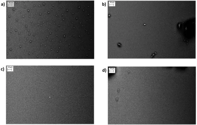
Figure 3. SEM image of (a) SMA, (b) SMB, (c) SMC and (d) SMD thin films at 500×.
that was still in the process of evaporation came into contact with the previous-ly-deposited layer at above-room temperature. Due to the thermal gradient de-crease during this second deposition, additional nuclei slowly grew into grains of a considerable size. These results are relevant because film defects, such as grains and impurities, can affect charge transport throughout the material. Efficient charge transport requires that charges move quickly from one molecule to another, rather than being trapped or dispersed. The presence of grains and im-purities can also affect molecular stacking, which is a key factor in mobility, leading to charge carriers moving through low- and even zero-conductivity paths. On the other hand, in the SMB and SMD thin films in Figure 3(b) &
DOI: 10.4236/ampc.2019.94007 77 Advances in Materials Physics and Chemistry
electrical behavior is expected to be superior in this film with respect to SMA,
SMB and SMD. Moreover, EDS analysis shows the presence of chemical ele-ments (see Figure 1) that constitute the molecules of both M2Pcs (M = Li, Na),
TTF and TCNQ dopants. This suggests that, in the growth process, the thin films were not degraded. These results are complemented by those obtained from IR spectroscopy, where the main functional groups found in organic semi-conductors are corroborated.
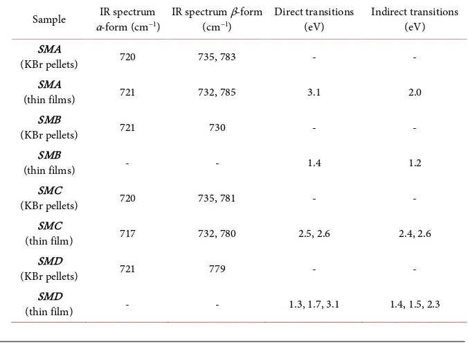
IR spectroscopy results from the films gave clear evidence of their thermal stability, which turns out to be excellent for doped M2Pcs.IR spectroscopy was
carried out to identify the interactions of M2Pc (M = Li, Na) macrocycles and the
dopant molecular units, as well as to establish the crystalline nature of the com-pounds [15] [16]. This is so because the IR spectrum of Pcs is strongly depen-dent on their chemical composition and crystalline structure. The bands corres-ponding to the Pc ring are mentioned in the experimental section [15] [16][17]
and shown in Figure 4 for KBr pellets. The bands responsible for C=N appear at 1481, 1334 and 1279 cm–1, while the bands located around 1160, 1119, 779 and
748 cm–1 result from the C-H interaction [15] [16]. The bands at 1606 and 1094
cm–1 result from a C=C stretch within the macrocyclic ring; other bands around
1440 and 875 cm–1 that represent various atomic interactions within the
macro-cyclic ring of M2Pc and the dopants were also found [17]. For doped
semicon-ductors SMA and SMB, the band related to the C=C interaction is located around 1077 cm−1 and the bands corresponding to the C-S bond of the TTF
mo-lecule used as a dopant were located at 840 and 780 cm−1 [18]. The TCNQ
[image:7.595.213.535.468.718.2]mo-lecule in doped semiconductors SMC and SMD has peaks around 1204, 1441 and 1597 cm−1 and is related to C=C-H bending, C-CN stretching and C=C ring
DOI: 10.4236/ampc.2019.94007 78 Advances in Materials Physics and Chemistry
stretching, respectively [19]. It is also possible to identify from IR spectroscopy the different crystalline structures α and β in the Pcs [19]. The α-form can be characterized by a band around 720 cm−1, while the β-form can be characterized
by two bands around 730 and 778 cm−1 [20]. From these studies, we can
deter-mine the phase and any significant chemical changes which may occur in these materials during thermal evaporation. In Table 1 and Figure 4, it can be ob-served that the SMA and SMC semiconductors originally showed both the
α-form and the β-form, and both crystalline forms remain after thin film deposi-tion. Their orientations are characterized by a herringbone structure, the main differences between them being the molecular overlapping areas in the thin films. In α type, molecular orientation is in the direction normal to the substrate surface, whereas the β molecules lie perpendicular to the substrate surface [21]. On the other hand, in the SMB and SMD materials, an amorphous structure is found in both semiconductor films. Figure 5 shows the XRD patterns of the films deposited on silicon wafers. The background due to scattering from the silicon substrate has been subtracted. According to the results obtained by IR spectroscopy, there is only some degree of crystallinity for the SMA and SMC
films and an amorphous structure for the SMB and SMD films. For SMA, a broad signal around 23˚ is observed, which is indicative of the partial amorph-ous character of this structure [22], the diffraction peak around 15˚ correspond-ing to the β phase [23]. On the other hand, the SMC film has the distinctive fea-tures of the M2Pc polymorphous structure, characterized by a single harp
[image:8.595.201.539.491.740.2]reflec-tion at 2θ of 6.9˚ [21]. This peak arises from the interlayer spacing of stacks of tilted molecules and this peak is the result of an α structure corresponding to the monoclinic system of the M2Pc doped crystals [21]. Figure 5 thus indicates the
Table 1. FTIR bands for powdered materials and thin films and bandgap transitions for films.
Sample α-form (cmIR spectrum −1)
IR spectrum β-form
(cm−1) Direct transitions (eV) Indirect transitions (eV)
SMA
(KBr pellets) 720 735, 783 - -
SMA
(thin films) 721 732, 785 3.1 2.0
SMB
(KBr pellets) 721 730 - -
SMB
(thin films) - - 1.4 1.2
SMC
(KBr pellets) 720 735, 781 - -
SMC
(thin film) 717 732, 780 2.5, 2.6 2.4, 2.6
SMD
(KBr pellets) 721 779 - -
SMD
DOI: 10.4236/ampc.2019.94007 79 Advances in Materials Physics and Chemistry
Figure 5. XRD patterns of SM films.
mainly amorphous character of all the films. This structural disorder is due to weak non-covalent interactions occurring during material deposition, which leads to each molecule’s environment not being identical to those of other mo-lecules within the solid system. In these amorphous semiconductors, structural defects can give raise to energetic levels located between the conduction (LUMO) and valence (HOMO) bands, which are called cargo traps. The presence of traps will affect the charge transport in the organic semiconductor and their optical bandgap.
The optical bandgap is a fundamental parameter to consider in the manufac-ture of devices for optoelectronics. The value of this bandgap is directly related to the electronic transition from the valence band to the conduction band in semiconductors. The electronic properties of semiconductors are related to the bandgap; for instance, in an organic diode, the bandgap controls the nature of the electroluminescence signal while, in a photovoltaic cell, it controls light ab-sorption efficiency. Figure 6 shows the Tauc plot used to calculate the optical bandgap for direct electronic transitions (αhν)2, as well as for indirect electronic
transitions (αhν)1/2. The distinction concerns the relative positions of the
mini-mum conduction band and the maximini-mum valence band energies. In a material with direct bandgap, both conditions occur for the same crystal momentum so that, during the transition, the electron shifts from the low energy band to the high band by absorbing or releasing a photon. In an indirect bandgap material, the minimal conduction band energy does not occur at the same crystal mo-mentum as the maximal valence band energy, being instead located at the edge area or next to it. During the transition, it is not possible for the electron to shift between the valence and conduction bands by only absorbing or releasing a photon; the transition should rather involve a phonon to ensure momentum conservation [24]. The obtained optical bandgap values are provided in Table 1, and although it is observed that the curves show a similar behavior for all films, for indirect transitions there is a slight decrease in the optical bandgap, due to the mainly amorphous morphology of the films. It is important to mention that all films present a bandgap in the range expected for organic semiconductors
DOI: 10.4236/ampc.2019.94007 80 Advances in Materials Physics and Chemistry
Figure 6. Direct (αhν)2 and indirect (αhν)1/2 optical bandgap determination for the
semi-conductor films.
due to the presence of sodium atoms in the phthalocyanine molecules, which are bigger than the lithium atoms in the remaining films. It seems that a bigger atomic size favors electronic transport between the orbitals of the atomic peri-phery. On the other hand, semiconductor films SMC and SMD with TCNQ do-pant show additional electronic bandgap transitions when compared with TTF-doped films. The doping effect of TCNQ may then be more efficient than that of TTF in SMC and SMD, even with their amorphous character, while the structural weakness of non-covalent interactions restricts orbital overlap from nearby molecules. Thus, electronic transport would be due to charge transfer between levels located in the M2Pc and the TCNQ molecules. It is worth noting
that the highest bandgap corresponds to the SMA film which, according to SEM observations, has a heterogeneous morphology with particles of considerable size. As mentioned above, this structure can affect electronic transport through the semiconductor, leading to a higher bandgap than those of the other semi-conductor films.
The spectral properties of the M2Pc are caused by an aromatic, cyclic
DOI: 10.4236/ampc.2019.94007 81 Advances in Materials Physics and Chemistry
Figure 7. Optical spectra of SM films.
B-band around 330 nm (for SMC and SMD films doped with TCNQ) or around 360 nm (for SMA and SMB thin films doped with TTF) [16]. The electronic
n-π* transition corresponds to a B-band indicating the fundamental absorption edge; the B-band is due to
( )
( )
*2u g
a
π
→eπ
and( )
( )
*2u g
b
π
→eπ
transitions[26] [27].
3.2. Device Characterization
In order to evaluate the behavior of the semiconductor films within an electronic device, the scattered heterojunctions: DSMA = glass/ITO/Li2Pc-TTF/Ag, DSMB
= glass/ITO/Na2Pc-TTF/Ag, DSMC = glass/ITO/Li2Pc-TCNQ/Ag and DSMD:
glass/ITO/Na2Pc-TCNQ/Ag devices were manufactured. The construction of the
devices included four silver electrodes in order to perform electrical measure-ments through the four-point collinear method, as shown in Figure 8. This type of arrangement involves four tips of equal spacing in a straight line at the center of the device; a current is applied to the outside tips and a voltage is measured from the central tips. The electrical behavior of the devices was analyzed by studying their current density-voltage (J-V) curves, obtained from the cur-rent-voltage (I-V) measurements. The goal of this analysis was to determine if the doped M2Pcs with alkali metals could function as semiconducting materials,
to find the effects of the different dopants on their behavior and to evaluate the differences that arise from using disodium versus dilithium.
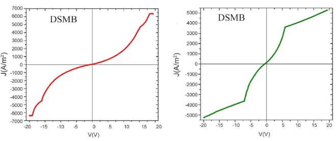
Figure 9 shows the comparison between the Na2Pc thin films. It can be
DOI: 10.4236/ampc.2019.94007 82 Advances in Materials Physics and Chemistry
[image:12.595.208.538.245.378.2]Figure 8. Four-point probe technique applied to the devices.
Figure 9.J-V curves for DSMB and DSMD.
current density, and it also has the lowest optical bandgap (see Table 1), al-though the DSMD device permits a higher number of electronic transitions. The rectifying-like behavior of the SMB and SMD devices could be attributed to the addition of dopants during the synthesis process. This process leads to the for-mation of a homogeneous material with a behavior resembling that of a p-n
junction. DSMB’s larger conductivity could be attributed to the formation of al-ternative paths for carrier conduction when doping a p-type organic semicon-ductor with TTF, as has been reported in previous studies [28]. On the other hand, DSMD’s behavior could also be related to the fact that, as has been dem-onstrated in other studies, TCNQ doping of p-type semiconductors, such as Na2Pc, could turn them into n-type semiconductors [29] [30]. The smaller
con-ductivity of DSMD in this work suggests a partial compensation of the p-type semiconductor with n-type material, leading to a reduction in charge carrier concentration.
Unlike the results obtained for the Na2Pc devices, the Li2Pc results (DSMA
and DSMC) show a symmetrical behavior with respect to the origin in their J-V
DOI: 10.4236/ampc.2019.94007 83 Advances in Materials Physics and Chemistry
Figure 10.J-V curves for DSMA and DSMC.
DSMC exhibits a current density-voltage behavior with a regular slope and an average resistance of 2203 Ω, indicating a semiconductor-like behavior. Howev-er, this device reaches a saturation point around 19 V, presenting an insulating behavior at higher voltages and restricting its possible applications to lower vol-tages. It has an ohmic behavior at small volvol-tages. On the other hand, DSMA has two different operating regimes. At low voltages, it is roughly ohmic until 6.5 V are reached, with an average resistance of 940 Ω. After that voltage, dynamic and overall resistance increases, as the current density increases at lower rates. The sudden change in slope suggests that the device enters a Space Charge Limited Current (SCLC) regime, governed by an exponential trap distribution, some-thing that doesn’t occur in DSMC. Parameters such as hole mobility (µ), ther-mally-excited hole concentration (p0), trap concentration per energy unit (P0)
and total trap concentration (Nt(e)) were calculated to verify the change from a
quasi-ohmic to an SCLC regime and to compare the device with other doped MPc thin films reported in the literature. Current density (J) in the ohmic re-gime is obtained from the following equation [31] [32]:
0
p e V J
d µ
= (1)
where, in addition to the previously defined parameters, e is the electronic charge, V is the voltage applied to the film and d is the film’s thickness. For the SCLC region, the equation for current density determination takes into consid-eration other factors [31] [32]:
1 0
2 1 0
l l
v l
L
V J N e
eP kT d
ε ε
µ ++
=
(2)
Nv being the effective density of states in the valence band, ε0 the vacuum
permittivity, ε the dielectric constant of the material, and k the Boltzmann con-stant. TL is the temperature parameter characterizing the trap distribution and l
is the slope in the ohmic regime zone, which can be obtained from dividing TL
by the local temperature. The films’ dielectric constant was obtained from [33]:
0
Cd A
ε ε
DOI: 10.4236/ampc.2019.94007 84 Advances in Materials Physics and Chemistry
where C is the film’s capacitance, determined from results obtained by Dumm et al. [12] for Li2Pc and A is the device’s transversal area. Finally, the total trap
concentration is given by [32]:
( ) 0
t e L
N =P kT (4)
The concentration of thermally-generated holes was obtained from Equation (1), hole mobility and concentration of traps per unit of energy were calculated from Equation (2) and the total trap concentration from Equation (4). Results shown in Table 2 were compared to those reported in the literature, regarding typical values for doped MPcs such as M = Ni, Cu, Co, Pb, Zn and falling in the ranges of SCLC behavior such as P0 between 8 × 1043 to 1.15 × 1047 J−1∙m−3 and 6
× 1020 to 9.3 × 1026 m−3 for N
t(e)[34] [35] [36] [37]. The μ value for DSMA is an
order of magnitude above that reported for ZnPcs (10−10 m2∙V−1∙s−1) [37], while
for DSMA the μ value is an order of magnitude below the interval reported for CuPcs (10−8 - 10−7 m2∙V−1∙s−1) [34] [35] [36]. Comparing the DSMA and DSMC
devices, it is clear that the one doped with TCNQ (DSMC) has a better response in low-voltage ranges, acting as a semiconductor with good resistance values and a J-V relationship that could be exploited in the future as it suggests an n-type organic semiconductor with metallic atoms suitable for optoelectronic devices. Once again, similarly to what happens with SMB, the doping of Li2Pc with TTF
(DSMA) changes the charge transportation paths [28]. SCLC behavior is corro-borated by comparison of the results to those found in the literature. The occur-rence of an SCLC regime opens the possibility for this organic semiconductor to be used in special applications requiring this electrical property.
Finally, the electrical behavior of the glass/ITO/TTF-TCNQ/Ag system was evaluated to determine the donor-acceptor ability of the dopants and their effect in the M2Pcs. As shown in Figure 11, the behavior in the −4 to 4 V range is that
of an electrical conductor, regardless of the applied polarity [38] [39]. It is worth mentioning that, at voltage magnitudes above 4 V, there is a sharp transition to an insulating behavior. From this, it is possible to deduce that the electrical be-havior of the DSM considered in this study is determined by the central metallic atoms in the M2Pcs, with a rectifying-like behavior when the molecule contains
sodium. The relatively lower conductivity values of DSMB and DSMD may be related to the chemical interaction of the sodium atoms with the macrocycle, where charge transfer could be high enough to block the free motion of elec-trons, because of the larger size of the central atom and the use of TTF dopant
[image:14.595.209.539.687.733.2][38]. On the other hand, the effect of lithium in DSMA and DSMC is enhanced by the use of the TCNQ dopant; the small size of the lithium atoms, combined with the presence of sulfur in TTF, could lead to anisotropic interactions [38], which themselves enhance the onset of the SCLC regime in DSMA.
Table 2. Results for electrical properties of DSMA.
p0 (m−3) µ (m2V−1s−1) P0 (J−1m−3) Nt(e) (m−3)
DOI: 10.4236/ampc.2019.94007 85 Advances in Materials Physics and Chemistry
Figure 11.I-V curve for Glass/ITO/TTF-TCNQ/Ag device.
4. Conclusion
Organic M2Pcs (M = Li, Na) semiconductors using TTF and TCNQ as dopants
were prepared. Thin films of these semiconductors were deposited by high va-cuum thermal evaporation, which is an adequate technique to prepare thin films of high purity and to manufacture heterojunction devices without chemical de-composition of the organic semiconductors that compose them. Organic semi-conductor thin films as deposited by evaporation have an amorphous structure. The structural disorder in the film will affect the electronic structure of the sem-iconductor and, specifically the energy of its molecular orbitals, which are no longer isoenergetic. Because of the above, doped semiconductors present indi-rect-type transitions involving photons and phonons. The amorphous structure promotes charge transport by hopping, which can be characterized as a diffusive process, where the charges hop between adjacent molecules. Glass/ITO/M2Pc (M
= Li, Na)-doped/Ag devices were manufactured. The electric behavior of the de-vices was evaluated from I-V measurements. The devices DSMB and DSMD
have a small rectifying effect in the −20 V to 20 V range, while behavior of the
DSMA and DSMC devices is of a quasi-ohmic nature. Apparently, the type of metal atom in the Pc macrocycle, the morphology of the films, as well as the doping effect of TTF and TCNQ, all have an important influence on the electric-al performance of the devices. The semiconductors synthetized from Na2Pc are
those that gave the best results regarding the optical bandgap and the behavior of the device manufactured with these semiconductors shows a rectifying-like I-V
characteristic, despite a smaller conductivity. On the other hand, the TCNQ do-pant considerably increased the current density transported along the Li2Pc
de-vices.
Acknowledgements
DOI: 10.4236/ampc.2019.94007 86 Advances in Materials Physics and Chemistry
Conflicts of Interest
The authors declare no conflicts of interest regarding the publication of this paper.
References
[1] Facchetti, A. (2007) Semiconductors for Organic Transistors. Materials Today, 10, 28-37.https://doi.org/10.1016/S1369-7021(07)70017-2
[2] Kumar, P., Jain, S.C., Kumar, V., Misra, A., Chand, S. and Kamalasanan, M.N. (2007) Current-Voltage Characteristics of an Organic Diode: Revisited. Synthetic Metals, 157, 905-907.https://doi.org/10.1016/j.synthmet.2007.08.021
[3] Melzer, C. and von Seggern, H. (2010) Enlightened Organic Transistors: Organic Light-Emitting Field-Effect Transistors Surpass the External Quantum Efficiency of Analogous Organic Light-Emitting Diodes. Nature Materials, 9, 470-472.
https://doi.org/10.1038/nmat2775
[4] Yoon-Heung, T., Ki-Beom, K., Hyoung-Guen, P., Kwang-Ho, L. and Jong-Ram, L. (2002) Criteria for ITO (Indium-Tin-Oxide) Thin Film as the Bottom Electrode of an Organic Light Emitting Diode. Thin Solid Films, 411, 12-16.
https://doi.org/10.1016/S0040-6090(02)00165-7
[5] Alamri, S.N., Joraid, A.A. and Al-Raqa S.Y. (2008) Structural and Optical Properties of Thermally Evaporated 1,4,8,11,15,18,22,25-Octahexylphthalocyanine Thin Films.
Journal of Taibah University for Science, 1, 35-42.
https://doi.org/10.1016/S1658-3655(12)60031-4
[6] Krull, C., Robles, R., Mugarza, A. and Gambardella, P. (2013) Site- and Orbit-al-Dependent Charge Donation and Spin Manipulation in Electron-Doped Metal Phthalocyanines. Nature Materials, 12, 337-343.https://doi.org/10.1038/nmat3547
[7] El-Nahass, M.M., Zeyada, H.M., Aziz, M.S. and El-Ghamaz, N.A. (2004) Structural and Optical Properties of Thermally Evaporated Zinc Phthalocyanine Thin Films.
Optical Materials, 27, 491-498.https://doi.org/10.1016/j.optmat.2004.04.010
[8] Soliman, H.S., El-Barry, A.M.A., Khosifan, N.M. and El Nahass, M.M. (2007) Structural and Electrical Properties of Thermally Evaporated Cobalt Phthalocyanine (CoPc) Thin Films. The European Physical Journal Applied Physics, 37, 1-9.
https://doi.org/10.1051/epjap:2006135
[9] Sánchez-Vergara M.E., Huerta-Francos, M., Menéndez-Huerta, M., Espinosa-Creel, M., Amelines-Sarria, O. and Santoyo-Salazar, J. (2015) Preparation of Hybrid Mate-rials Containing M(II)Pc (M = Fe, Co, Ni)/Nylon Films with Optical and Electrical Properties. Advances in Materials Physics and Chemistry, 5, 271-280.
https://doi.org/10.4236/ampc.2015.57026
[10] Wachtel, H., Wittmann, J.C., Lotz, B. and André, J.-J. (1993) Polymorphism of Li-thium Phthalocyanine Thin Films. Synthetic Metals,61, 139-142.
https://doi.org/10.1016/0379-6779(93)91211-J
[11] Brinkmann, M., Wittmann, J.C., Chaumont, C. and André, J.-J. (1997) Effects of Solvent on the Morphology and Crystalline Structure of Lithium Phthalocyanine Thin Films and Powders. Thin Solid Films, 292, 192-203.
https://doi.org/10.1016/S0040-6090(96)09087-6
[12] Dumm, M., Lunkenheimer, P., Loidl, A., Assmann, B., Homborg, H. and Fulde, P. (1996) Charge Transport in Lithium Phthalocyanine. The Journal of Chemical Physics, 104, 5048-5053.https://doi.org/10.1063/1.471134
DOI: 10.4236/ampc.2019.94007 87 Advances in Materials Physics and Chemistry
Amorphous Dilithium Phthalocyanine Using the Tauc and Cody Models.
Molecules, 17, 10000-10013.https://doi.org/10.3390/molecules170910000
[14] Nieto, E., Fernández, F., Durán, P. and Moure, C. (1994) Películas delgadas: Fabricación y aplicaciones. Boletín de la Sociedad Española de Cerámica y Vidrio, 33, 245-258.
[15] Touka, N., Benelmadjat, H., Boudine, B., Halimi, O. and Sebais, M. (2013) Copper Phthalocyanine Nanocrystals Embedded into Polymer Host: Preparation and Structural Characterization. Journal of the Association of Arab Universities for Basic and Applied Sciences, 13, 52-56.https://doi.org/10.1016/j.jaubas.2012.03.002
[16] El-Nahass, M.M., Abd-El-Rahman, K.F., Al-Ghamdi, A.A. and Asiri, A.M. (2004) Optical Properties of Thermally Evaporated Tin-Phthalocyanine Dichloride Thin Films, SnPcCl2. Physica B: Condensed Matter, 344, 398-406.
[17] Hart, M.M. (2009) Cationic Exchange Reactions Involving Dilithium Phthalocya-nine. Thesis for the Degree of Master of Science, Wright State University.
[18] Kim, Y.-I., Jeong, C.-K., Lee, Y.-M. and Choi, S.-N. (2002) Synthesis and Charac-terization of Tetrathiafulvalene (TTF) and 7,7,8,8-Tetracyanoquinodimethane (TCNQ) Compounds with PdX2 (X = Cl, NO3 and Hexafluoroacetylacetonate).
Bulletin of the Korean Chemical Society, 23, 1754-1758.
https://doi.org/10.5012/bkcs.2002.23.12.1754
[19] Galfo, L., Cordeiro, M.R., Freitas, A.R., Moreira, W.C., Girotto, E.M. and Zucolotto, V. (2010) The Effects of Temperature on the Molecular Orientation of Zinc Phthalocyanine Films. Journal of Materials Science, 45, 1366.
https://doi.org/10.1007/s10853-009-4094-3
[20] El-Nahass, M.M., Farag, A.M., Abd El-Rahman, K.F. and Darwish, A.A.A. (2005) Dispersion Studies and Electronic Transitions in Nickel Phthalocyanine Thin Films.
Optics & Laser Technology, 37, 513-523.
https://doi.org/10.1016/j.optlastec.2004.08.016
[21] Della Pirriera, M., Puigdollers, J., Voz, C., Stella, M., Bertomeu, J. and Alcubilla, R. (2009) Optoelectronic Properties of CuPc Thin Films Deposited at Different Sub-strate Temperatures. Journal of Physics D: Applied Physics, 42, 102-145.
https://doi.org/10.1088/0022-3727/42/14/145102
[22] El-Nahass, M.M., Ammar, A.H., Farag, A.A.M., Atta, A.A. and El-Zaidia, E.F.M. (2011) Effect of Heat Treatment on Morphological, Structural and Optical Proper-ties of CoMTPP Thin Films. Solid State Sciences, 13, 596-600.
https://doi.org/10.1016/j.solidstatesciences.2010.12.032
[23] Vasseur, K., Rand, B.P., Cheyns, D., Froyen, L. and Heremans, P. (2011) Structural Evolution of Evaporated Lead Phthalocyanine Thin Films for Near-Infrared Sensi-tive Solar Cells. Chemistry of Materials, 23, 886-895.
https://doi.org/10.1021/cm102329v
[24] El-Nahass, M.M., Sallam, M.M. and Alí, H.A.M. (2005) Optical Properties of Ther-mally Evaporated Metal-Free Phathalocyanine (H2Pc) Thin Films. International
Journal of Modern Physics B, 19, 4057-4071.
https://doi.org/10.1142/S0217979205032632
[25] García-Moreno, G. (2012) Pi-Conjugated Organic Semiconductor Based on Thio-phene. A Theorical Study. Doctoral Thesis, University of Jaén, School of Experi-mental Science.
DOI: 10.4236/ampc.2019.94007 88 Advances in Materials Physics and Chemistry
[27] Novotny, M., Bulir, J., Bensalah-Ledoux, A., Guy, S., Fitl, P., Vrnata, M., Lancok, J. and Moine, B. (2014) Optical Properties of Zinc Phthalocyanine Thin Films Pre-pared by Pulsed Laser Deposition. Applied Physics A, Materials, Science & Processing, 117, 377-381.https://doi.org/10.1007/s00339-014-8474-4
[28] Sánchez-Vergara, M.E, Leyva-Esqueda, M., Alvárez-Bada, J.R., García-Montalvo, V., Rojas-Montoya, I.D. and Jiménez-Sandoval, O. (2015) Optical and Electrical Properties of TTF-MPcs (M = Cu, Zn) Interfaces for Optoelectronic Applications.
Molecules, 20, 21037-21049.https://doi.org/10.3390/molecules201219742
[29] Zhang, J., Gu, P., Long, G., Ganguly, R., Li, Y., Aranti, N., Yamadac, H. and Zhang, Q. (2016) Switching Charge-Transfer Characteristics from p-Type to n-Type through Molecular “Doping” (Cocrystallization). Chemical Science, 7, 3851-3856.
https://doi.org/10.1039/C5SC04954G
[30] Xie, M., Zhang, S., Cai, B., Zou., Y. and Zeng, H. (2016) N- and p-Type Doping of Antimonene. RSC Advances, 6, 14620-14625.https://doi.org/10.1039/C5RA25572D
[31] Hassan, A.K. and Gould, R.D. (1993) The Interpretation of Current Density-Voltage and Activation Energy Measurements on Freshly Prepared and Heat-Treated Nickel Phthalocyanine Thin Films. International Journal of Electronics,74, 59-65.
https://doi.org/10.1080/00207219308925813
[32] Sánchez-Vergara, M.E., Medrano-Gallardo, D., Vera-Estrada, I.L. and Jiménez-Sandoval, O. (2018) Optical Absorption and Electrical Properties of MPc (M = Fe, Cu, Zn)-TCNQ Interfaces for Optoelectronic Applications. Journal of Physics and Chemistry of Solids, 115, 373-380.
https://doi.org/10.1016/j.jpcs.2018.01.005
[33] Dongol, M., El-Nahass, M.M., El-Denglawey, A., Abuelwafa, A.A. and Soga, T. (2016) Alternating Current Characterization of Nano-Pt(II) Octaethylporphyrin (PtOEP) Thin Film as a New Organic Semiconductor. Chinese Physics B, 25, Article ID: 067201.
[34] Gravano, S., Hassan, A.K. and Gould, R.D. (1991) Effects of Annealing on the Trap Distribution of Cobalt Phthalocyanine Thin Films. International Journal of Elec-tronics, 70, 477-484.https://doi.org/10.1080/00207219108921297
[35] Gould, R.D. (1985) Electrical Measurements on Evaporated Thin Films of Copper Phthalocyanine. Thin Solid Films, 125, 63-69.
https://doi.org/10.1016/0040-6090(85)90396-7
[36] Gould, R.D. (1996) Structure and Electrical Conduction Properties of Phthalocya-nine Thin Films. Coordination Chemistry Reviews, 156, 237-274.
https://doi.org/10.1016/S0010-8545(96)01238-6
[37] Kayunkid, N., Rangkasikorn, A., Saributr, C. and Nukeaw, J. (2016) Growth and Characterizations of Tin-Doped Zinc-Phthalocyanine Prepared by Thermal Co-Evaporation in High Vacuum as a Novel Nanomaterial. Japanese Journal of Ap-plied Physics, 55, 02BB12.https://doi.org/10.7567/JJAP.55.02BB12
[38] Bryce, M.R. (1995) Current Trends in Tetrathiofulvalene Chemistry: Towards In-creased Dimensionality. Journal of Materials Chemistry, 5, 1481-1496.
https://doi.org/10.1039/jm9950501481
[39] Hünig, S. (1995) N,N’-Dicyanoquinone Diimines (DCNQTs): Unique Acceptors for Conducting Materials. Journal of Materials Chemistry, 5, 1469-1479.