HYBRID PHOTONIC CRYSTAL CAVITY BASED LAYERS
Athanasios-Alexandros Liles
A Thesis Submitted for the Degree of PhD
at the
University of St Andrews
2017
Full metadata for this item is available in
St Andrews Research Repository
at:
http://research-repository.st-andrews.ac.uk/
Please use this identifier to cite or link to this item:
http://hdl.handle.net/10023/12081
This item is protected by original copyright
Hybrid Photonic Crystal Cavity Based Lasers
Athanasios Alexandros Liles
This thesis is submitted in partial fulfilment for the degree of PhD
at the
University of St Andrews
i
Declarations
I, Athanasios Alexandros Liles, hereby certify that this thesis, which is approximately 40000 words in length, has been written by me, and that it is the record of work carried out by me, or principally by myself in collaboration with others as acknowledged, and that it has not been submitted in any previous application for a higher degree.
I was admitted as a research student in September, 2013 and as a candidate for the degree of Doctor of Philosophy in September, 2013; the higher study for which this is a record was carried out in the University of St Andrews between 2013 and 2017.
Date: Signature of candidate:
I hereby certify that the candidate has fulfilled the conditions of the Resolution and Regulations appropriate for the degree of Doctor of Philosophy in the University of St Andrews and that the candidate is qualified to submit this thesis in application for that degree.
Date: Signature of supervisor:
In submitting this thesis to the University of St Andrews I understand that I am giving permission for it to be made available for use in accordance with the regulations of the University Library for the time being in force, subject to any copyright vested in the work not being affected thereby. I also understand that the title and the abstract will be published, and that a copy of the work may be made and supplied to any bona fide library or research worker, that my thesis will be electronically accessible for personal or research use unless exempt by award of an embargo as requested below, and that the library has the right to migrate my thesis into new electronic forms as required to ensure continued access to the thesis. I have obtained any third-party copyright permissions that may be required in order to allow such access and migration, or have requested the appropriate embargo below.
The following is an agreed request by candidate and supervisor regarding the publication of this thesis:
PRINTED COPY: No embargo on print copy.
ELECTRONIC COPY: No embargo on electronic copy.
ABSTRACT AND TITLE EMBARGOES: I agree to the title and abstract being published.
Date:
iii
Acknowledgements
Given the chance, I would like to thank a number of people who were involved in the conduction of my PhD and the completion of this thesis.
To begin with, I would like to express my sincere gratitude to my supervisor, Dr Liam in (William Whelan-Curtin), not only for offering me the opportunity to work in his research group and guiding me through this project, but also for always trying to be available for long discussions and willing to share his expertise and inspiring ideas. In addition, I am highly indebted to Dr Kapil Debnath and Dr Alfredo Gonzalez-Fernandez for their technical and scientific assistance and guidance, as well as for their patience and the significant amount of time they spent with me during their presence in St Andrews. Special thanks go to Dr Stephen Hegarty from Cork Institute of Technology (CIT) and Tyndall National Institute for the discussions and suggestions, and to Andrei Bakoz for helping me with the laser measurements and with my staying in Cork.
Moreover, I would like to thank my colleagues and friends in the School of Physics and Astronomy of the University of St Andrews for being most helpful and creating a pleasant working environment. I have to particularly thank everyone in the Nanophotonics and Synthetic Optics groups especially Dr Andrea DiFalco, Dr G.R. Chinna Devarapu and Changyu Hu and Dr N. Klaus Metzger. I would like to express my special appreciation to Mr Steve Balfour, Mr Callum Smith, Mr Graeme Beaton, and Mr Chris Watson for keeping the cleanroom and all its equipment in good working order at all times. I would also like to say thanks to Professor Dries Van Thourhout (Ghent University) for his time and effort in reading and improving this thesis.
v
List of Publications
Journal Articles
x K. Debnath, R. Moore, A. Liles, L. O'Faolain, "Toolkit for Photonic Integrated Circuits Based on Inverted Rib Waveguides", Journal of Lightwave Technology, 33, 19, p. 4145-4150 (2015) x A. A. Liles, K. Debnath, L. O'Faolain, "Lithographic wavelength control of an external cavity laser with a silicon photonic crystal cavity-based resonant reflector", Optics Letters, 41, 5, p. 894-897 (2016)
Conference Proceedings
x A. Liles, K. Debnath, L. O'Faolain, "External-Cavity Hybrid Laser with Silicon Photonic
Crystal Cavity-based Resonant Reflector", 2015 IEEE 12th International Conference on Group IV Photonics (GFP)
x A. A. Gonzalez-Fernandez, A. A. Liles, S. Persheyev, K. Debnath, L. O'Faolain, "Wavelength-controlled external cavity laser with a silicon photonic crystal resonant reflector", Proc. SPIE 9753, Optical Interconnects XVI, 975317 (2016)
x A. P. Bakoz, A. A. Liles, E. A. Viktorov, L. O'Faolain, T. Habruseva, G. Huyet, S. P. Hegarty, "Lasing dynamics of photonic crystal reflector laser", Proc. SPIE 9892, Semiconductor Lasers and Laser Dynamics VII, 989204 (2016)
x A. P. Bakoz, A. A. Liles, E. A. Viktorov, L. O'Faolain, G. Huyet, S. P. Hegarty, "Photonic crystal reflector laser", 2016 International Conference Laser Optics (LO)
x A. A. Liles, A. P. Bakoz, A. A. Gonzalez-Fernandez, T. Habruseva, S. Persheyev, G. Huyet,
S. P. Hegarty, L. O'Faolain, "Hybrid Photonic Crystal Lasers", 2016 18th International
Conference on Transparent Optical Networks
x A. A. Liles, A. A. Gonzalez-Fernandez, L. O'Faolain, "III-V/Silicon External Cavity Laser with Photonic Crystal Cavity Reflector", 12th International Symposium on Photonic and
Electromagnetic Crystal Structures PECS XII (2016)
x A.A. Liles, A. P. Bakoz, A. A. Gonzalez-Fernandez, T. Habruseva, G. Huyet, S. P. Hegarty,
vi Conferences Attended
x UK Silicon Photonics Conference (Showcase), November 2013, Southampton
x IEEE 12th International Conference on Group IV Photonics (GFP), August 2015, Vancouver
x 12th International Symposium on Photonic and Electromagnetic Crystal Structures
(PECS XII), July 2016, York
vii
Abstract
In recent years, Silicon Photonics has emerged as a promising technology for cost-effective fabrication of photonic components and integrated circuits, the application of which is recently expanding in technological fields beyond tele- and data-communications, such as sensing and biophotonics. Compact, energy-efficient laser sources with precise wavelength control are crucial for the aforementioned applications. However, practical, efficient, electrically-pumped lasers on Silicon or other group IV elements are still absent, owing to the indirect bandgap of those materials. Consequently, the integration of III-V compounds on Silicon currently appears to be the most viable route to the realization of such lasers.
In this thesis, I present and explore the potential of an External Cavity (EC) hybrid III-V/Silicon laser design, comprising a III-V-based Reflective Semiconductor Optical Amplifier (RSOA) and a Silicon reflector chip, based on a two-dimensional Photonic Crystal (PhC) cavity vertically coupled to a low-refractive-index dielectric waveguide. The vertically coupled system functions as a wavelength-selective reflector, determining the lasing wavelength. Based on this architecture mW-level continuous-wave (CW) lasing at room temperature was shown both in a fiber-based long cavity scheme and die-based short cavity scheme, with SMSR of > 25 dB and > 40 dB, respectively.
ix
Contents
Declarations ... i
Acknowledgments ... iii
List of Publications ... v
Abstract ... vii
Contents... ix
Chapter 1 Light Sources for Optical Interconnects ... 1
1.1 Introduction ... 1
1.2 Laser Sources for Optical Interconnects: The State of the Art ... 4
1.2.1 Direct Mounting ... 6
1.2.2 Wafer Bonding-Based Heterogeneous Integration ... 6
1.2.3 Direct Hetero-Epitaxial Growth ... 8
1.2.4 External Cavity Hybrid Integration ... 9
1.3 Aim of the Thesis ... 10
1.4 Thesis Content ... 11
References ... 12
Chapter 2 Background ... 21
2.1 Introduction ... 21
2.2 Photonic Crystals ... 21
2.2.1 Photonic Band gap in a 1D Photonic Crystal ... 22
2.2.2 Two-Dimensional Photonic Crystals ... 24
2.3 Photonic Crystal Cavities ... 26
2.4 Vertically Coupled Waveguide-Photonic Crystal Cavity as a Resonant Reflector ... 31
2.4.1 The Concept ... 31
x
2.4.3 The Device ... 35
2.5 Laser Cavity with Resonant Reflector Based on Waveguide Vertically Coupled to a Photonic Crystal Cavity ... 37
2.6 Discussion ... 42
References ... 43
Chapter 3 Fabrication Tools and Processes ... 47
3.1 Introduction ... 47
3.2 Sample Fabrication ... 47
3.3 Photolithography ... 50
3.4 Ion Implantation ... 52
3.5 Electron-Beam Lithography ... 53
3.6 Reactive Ion Etching ... 57
3.7 Electron-Beam Physical Vapour Deposition ... 59
3.7.1 Electron-Beam Physical Vapour Deposition ... 59
3.7.2 Electron-Beam Physical Vapour Deposition for Anti-Reflection Coatings ... 61
3.8 Conclusion ... 63
References ... 64
Chapter 4 Long External Cavity Laser Configuration ... 65
4.1 Introduction ... 65
4.2 The Laser Cavity... 66
4.3 Experimental Setup and Laser Characterization ... 67
4.4 Lithographic tuning ... 70
4.5 Discussion ... 71
References ... 74
Chapter 5 Compact External Cavity Laser Configuration ... 77
5.1 Introduction ... 77
5.2 The Laser Cavity... 78
5.2.1 Design Description ... 78
5.2.2 Design Considerations ... 79
xi
5.3.1 Laser Characterization ... 83
5.3.2 Alignment Tolerance ... 86
5.3.3 Thermal Stability ... 89
5.4 Discussion ... 94
References ... 97
Chapter 6 Compact External Cavity Laser for Direct Frequency Modulation and Future Work ... 101
6.1 Introduction ... 101
6.2 Wavelength Tuning in Photonic Crystal Cavity Based Reflector ... 103
6.3 The Laser Cavity... 105
6.3.1 Design Description ... 105
6.3.2 Tunable Resonant Reflector Fabrication ... 107
6.4 Experimental Setup and Characterization ... 110
6.4.1 Direct Frequency Modulation ... 112
6.5 Discussion ... 114
6.6 Improvements and Future Work ... 115
6.6.1 Optimization of Direct Frequency Modulation ... 116
6.6.2 Improvement of the Compact EC Configuration ... 117
6.6.3 Bonding and EC Laser Arrays ... 118
References ... 120
Chapter 7 Conclusion ... 125
References ... 128
Appendix A Ion Implantation Process Flow and Ion Implantation Doses (for the process followed in Tyndall National Institute) ... 131
List of Figures ... 137
1
Chapter 1
Light Sources for Optical Interconnects
1.1 Introduction
Access to Information and Communications Technology (ICT) platforms by anyone, anywhere and at any time is becoming of increasingly high importance [1]. This demand reveals a distinct characteristic of our society: its reliance on a perpetual transfer of knowledge and information. An inevitable consequence of this fact, in combination with the advancement of technology, has been the expansion of the Internet and its infrastructure (with more than 3.5 billion estimated Internet users in March 2017 [2]), and the development of distributed computing applications. This inexorable bandwidth (visualized in Fig. 1.1) has recently been reflected upon the establishment of a new generation of network services, known as cloud services. Cloud services are made available to users through cloud computing servers, and therefore are based on the concentration of data storage and computational power in data centers. Data centers are huge facilities housing interconnected computer systems and associated components, which are in turn responsible for the distribution of data to the end-users. In such architectures, fast processing speeds and low latency are crucial: according to Google, for example, an additional latency of 0.5 sec when loading a search result page causes a 20% decrease in search traffic [3]. Given the enormous amounts of data that need to be handled, the above restrictions impose significant challenges on the ICT and data communication infrastructure, especially in terms of power consumption. With current estimates showing that the operation of the Internet amounts to ~5% of the global electricity use [4] (and suggestions that the production and use of ICT might
2016 2017 2018 2019 2020 2021
0 5 10 15 20 25 30
1.03
27.4
Exabytes per Month
92% CAGR 2016-2021
Figure 1.1 Projected IPv6 Mobile Data Traffic Forecast by CISCO (column chart with data from Cisco
2
grow to ~20% of the global supply by 2030 [6]) the necessity for faster and more energy efficient computer and communication systems is apparent.
To date, improvement in the performance of Integrated Circuits (ICs) and microprocessors has been achieved by scaling down the size of the transistors that comprise them, following the trend predicted by G. Moore in 1965 that the on-chip transistor density would double approximately every two years [7]. However, as the number of transistors per unit area of circuit board increases, so does the complexity and packaging density of the interconnect systems (i.e. the network of metal wires that transport data and synchronization information on and to the chip). A typical microprocessor chip today contains over 10 km of metal tracks in a three-dimensional interconnect network spread over multiple separate layers [3]. The bandwidth of an electrical wire is proportional to its cross-section and inversely proportional to the square of its length [8]. As more and more transistors are packed into a given area on a chip, the interconnections become progressively longer and more complicated, a situation that leads to the appearance of several problems, such as increased parasitic capacitance (and consequently power consumption [9]), higher cross-talk noise [10], and eventually higher signal propagation delay. The intra-/inter-chip communication delay, known a [10], has become considerably high (comparable to the computation delay), leading electrical interconnects to hit a wall in terms of high-speed, energy efficient performance. The enforced shift towards multicore chips and parallel operation, aiming to maintain the processor power dissipation below a certain ceiling/threshold, further aggravates the problem, as it increases the required link length and imposes additional restraints on the supported bitrate/available bandwidth [11]. Numerous approaches have been suggested to overcome the delay, power and bandwidth limitations of traditional electrical interconnects, mostly related to the alteration of the physical means of the links (e.g. superconducting wires, graphene nanoribbons, optical waveguides etc [12]). The project described in this thesis explores the alternative solution of optical interconnects.
With the initial demonstrations of optical transmission taking place in
the first fiber-optics-based system for live telephone traffic established in 1977 in Chicago [13], optical communications nowadays dominate the backbone and backhaul networks of the telecommunication systems. However, the employment of optics as an alternative physical approach for short-range networks (datacommunication and interconnects) was not proposed until 1984, when J. W. Goodman [14], [15] suggested using photons instead of electrons as carriers of information in order to hammer away most if not all the issues encountered by electrical interconnects [16]. More specifically, as photons are electrically neutral and massless particles, they can propagate in transparent media (i.e. with no electrical resistance or capacitance the RC time constant and ohmic losses are not an issue) with low heat and power dissipation, and little cross-talk [10]. Furthermore, the high frequencies of optical carrier waves (1014 Hz)
3 However, substituting electrical interconnects with optical equivalents is an endeavour that involves formidable cost and practical challenges. In this scenario, the factors that need to be primarily considered are the fabrication and packaging cost, the ease of integration with the existing infrastructure and the power consumption of the optical interconnects [11], [17]. Silicon Photonics has emerged as an appealing solution, aiming to tackle the aforementioned challenges by providing a common platform for both electronics and optics [18]. As Silicon is the basic material used by the electronics industry, the use of Silicon for optical interconnects offers the potential for integration with the existing electronic circuitry. Additionally, Silicon Photonics can take advantage of the mature CMOS process technology of materials with well-known properties, to deliver low-cost, high-performance optical components and Photonic Integrated Circuits
The Silicon Photonics research was initiated in the
mid-Bennett and Lorenzo [19], [20]. Ever since, many keystone interconnect components that can be employed in real-life applications have been demonstrated on Silicon: extremely low-loss waveguides [21], [22], (de)multiplexers [23], ultra-fast modulators [24] and high-bandwidth photodetectors [25]. One of the major research axes of the field has always been the achievement of as low power consumption as possible, in order to comply with the projected performance requirements (indicatively, the International Technology Roadmap for Semiconductors forecasts the need for an individual device energy consumption of > 20 fJ/bit for intra-chip communication and >10 fJ/bit for on-chip interconnects, by 2022 [12]). As the nodes with the highest power consumption in an optical interconnect are the light source and the modulator [26], serious effort has been put in the implementation of compact, energy-efficient active optical devices on Silicon. A significant boost towards that direction was the demonstration of optical components based on micro-photonic resonators, such as ring resonators or photonic crystal cavities. Owing to their ability to strongly confine light spatially and temporally, optical resonators not only offer reduced footprint that makes them appropriate for chip-scale integration, but also exhibit ultra-low switching energies, proving excellent candidates for low-power consumption (sub-pJ/bit) modulation [27], [28], [29], [30]. Even though matching the emitted wavelength of a laser source to the resonances of an optical modulator of this type requires additional complexity and control electronics that have so far hindered their wide deployment in practical applications, their wavelength-selective and energy-efficient nature renders them particularly suitable for WDM systems, and therefore key to satisfying the requirements of future interconnect systems [31].
Energy
k
Valence Band Conduction band
Indirect Band Gap
4
However, despite the fact that the Silicon Photonics technology is constantly refined to meet the evolving application requirements, there still exist fundamental constraints that impede its progress in optical interconnect systems. A most prominent example is the inferior light emission spontaneous or stimulated from Silicon, stemming from the indirect band gap of Group IV semiconductors (Fig. 1.2). As a result, the most essential building block of an optical communication system is still absent from the Silicon Photonics toolkit.
Driven by the above goals, in this thesis, I demonstrate an External Cavity (EC) hybrid III-V/Silicon laser design, utilizing a Photonic Crystal cavity-based resonant reflector, with performance characteristics that align with the requirements of datacommunication networks.
1.2 Laser Sources for Optical Interconnects: The State of the Art
Based on the discussion of Section 1.1, it is apparent that there are three Figures of Merit (FoM) that drive the development of optical transceivers for intra-datacenter transmission links and high performance computational systems [26]:
x Gbps/mm3 and Gbps/mm2 (expressing the bandwidth per unit volume and surface of optical
circuitry)
x J/bit (quantifying the energy consumption of the links)
x $/Gbps (expressing the transceiver cost per Gbps of transmitted information).
The power consumption (and consequently the cost) in the above scenarios is roughly proportional to the frequency/speed of modulation of an optical carrier. As a result, optical systems that support multiple wavelengths are preferable from an energy point of view. WDM allows sending multiple optical frequencies over the same medium, offering the scalability (in the number of communication channels per physical connection) and the inherent parallelism needed for chip-scale and on-chip interconnections.
The nature of wavelength multiplexing systems [16], [32] along with the operating environment and cost structure of datacentres [26], impose rather strict requirements that the optical source candidates for Silicon optical interconnects should satisfy [33]: emission at around 1.3 or 1.55 m for direct connectivity with fiber optical networks, electrically pumped lasing for high integration density, high wall-plug efficiency and low energy cost for data transmission, and integratability on Silicon with CMOS-compatible fabrication processes for low-cost, large-scale manufacturing. Additionally, the light sources for Silicon WDM datacommunication networks should exhibit narrow linewidths and precise wavelength registration/stability over a wide temperature range to facilitate tighter channel spacing (and consequently larger aggregate bandwidth at a given frequency band).
5 significantly limits their emission efficiency, considerably impeding the development of an on-chip light source on them. Aiming at improving the radiative properties of those materials, a few promising options have been extensively researched in the recent past. More specifically, solutions based on ultra-thin Silicon p-n junctions [34], porous Silicon [35], and extremely pure bulk Silicon [36] have been proposed to achieve electroluminescence from Silicon. Other solutions involve the engineering of the band structure of Silicon [10], strain induced by implantation [37], Raman scattering [38] or rely on quantum confinement effects in Silicon nanocrystals [39], while an alternative solution involves the Erbium (Er) doping of Group IV material systems for optical gain and luminescence [40], [41], [42]. Finally, an approach that has drawn significant attention is the use of strained Germanium (Ge) [43] or Ge alloys (e.g. GeSn) on Silicon for lasing [44], [45]. Be that as it may, all the devices based on the aforementioned solutions are at a preliminary stage and their performance is still far from the standards set by the Silicon Photonics industry. As a result, their employment in real-life interconnect applications in the immediate future appears to be a rather ambitious concept/outlook.
With the demand for higher bandwidth in optical interconnects being ever-growing, the need for an energy-efficient, electrically pumped laser solution that would be integratable with Silicon Photonics PICs appears imperative. III-V compound semiconductors have been traditionally used for highly efficient, electrically injected lasers, owing to their direct bandgap and high material gain. Integrating the III-V functionality on the Silicon Photonics platform therefore, currently appears to be the most viable and practical route to high-efficiency sources for chip-scale applications [33], [46]. This task, however, is particularly challenging due to the significant lattice constant and thermal expansion coefficient mismatch between Silicon and III-V semiconductors. This mismatch is responsible for a high defect density (e.g. threading or misfit dislocation on the interface) and consequently high power losses, hindering in this way the direct growth of III-V materials on Silicon.
6
1.2.1 Direct Mounting
One of the easiest and most straightforward ways to achieve (single-mode) laser integration with a Silicon chip is by packaging the chip and a pre-fabricated III-V laser in the same module. This method (referred to as direct mounting) is defined by the direct mounting of individual laser diode dies on a Silicon or Silicon-on-Insulator (SOI) wafer by means of solder bumps [52], and is broadly used in components for long-haul systems today (where III-V lasers are packaged together with e.g. LiNbO3 modulators). This approach allows the testing of the devices prior to
integration and the independent development and optimization of the two components for optimal performance and high yield. In this way, it is possible to maintain the superior characteristics of the III-V laser chip (e.g. high wall-plug efficiency of ~20% [33]), as well as good thermal dissipation.
The main issue with this option is the requirement for submicron precision alignment for efficient coupling of light from the III-V component to the on-chip waveguide, which is time consuming, increases the assembly cost, and often results in degraded performance due to coupling losses. Moreover, the optical feedback from the interface between the two components (and in general from any coupling point) is detrimental to the performance of the laser, dictating the need for more complicated packaging approaches (e.g. using micro-optics and optical isolators, as suggested by Luxtera and Tyndall [53, 54]). All the above, in combination with the size of the solder bumps, limit the integration density and the scalability of this approach, and thus make it less attractive for low-cost applications.
1.2.2 Wafer Bonding-Based Heterogeneous Integration
An alternative approach, referred to as wafer bonding-based heterogeneous integration, describes the integration of an unpatterned III-V epi-layer on patterned Silicon circuits (wafers or chips) via a number of different bonding techniques. In this scheme, the light generated in the III-V material is typically evanescently coupled into the Silicon circuits. Upon the completion of the bonding process, the III-V epi-layer is lithographically patterned and the composite system is further processed for the fabrication/definition of the integrated laser. Performing the bonding prior to the laser processing offers a significant advantage in terms of bonding accuracy: the misalignment is determined by the lithographic error between the Silicon and III-V patterning, rather than by the III-V die placement accuracy, rendering this approach superior to direct mounting integration.
7 a result, die-to-wafer bonding appears to be favourable for the integration of III-V materials on Silicon. Apart from the above classification, the bonding methods can be further divided to direct and indirect bonding, based on whether a buffer/bonding/insertion/intermediate layer is used between the III-V stack and Silicon.
Direct bonding is defined by bringing polished, flat and ultra-clean wafers (or dies) into direct contact for the formation of strong interfacial Van der Waals bonds. Typical examples include molecular bonding using wet chemistry (for hydrophobic or hydrophilic surface treatment) and oxygen plasma-assisted low temperature molecular bonding (hydrophilic surface treatment) [55, 56]. Another interesting example of direct bonding employs fusion bonding at low temperatures (300 oC) to obtain a conductive hetero-interface that allows for vertical carrier
injection [57]. However, achieving good bonding quality with this method requires ultraclean conditions and atom-scale smoothness of the surfaces, resulting in a rather complex fabrication process [58], while it typically exhibits a low potential yield and reproducibility.
Indirect bonding employs metal or polymers like divinylsiloxane-benzocyclobutane (DVS-BCB) as adhesive layers and is therefore referred to as metal-assisted and BCB-assisted bonding, respectively. Metal-assisted bonding typically requires low bonding temperatures and relatively relaxed cleanliness conditions. It allows for effective thermal dissipation and potentially a low resistance Ohmic contact at the interface between Silicon and the bonded layers. The main issue with this approach is that the bonding metal can cause strong light absorption and potential metal contamination. In order to overcome these issues, the removal of the bonding metal from the coupling area (Fig. 1.3a) [59] and the use of additional conductive adhesive layers (e.g.
(a)
(b)
[image:22.612.154.489.400.624.2](c)
Figure 1.3 (a) Illustration of the cross-section of InGaAsP/Silicon hybrid laser based on metal bonding
8
Indium Tin Oxide ITO, shown in Fig. 1.3b) [60] have been proposed. BCB-assisted bonding is defined by the use of a BCB buffer layer between the III-V stack and the Silicon for adhesion purposes. BCB exhibits high bond strength, low refractive index and low curing temperature, and can compensate for the surface roughness between the two materials, relaxing the bonding tolerance compared to molecular bonding [62]. A major issue with this approach is the heat dissipation, as BCB exhibits poor thermal conductivity (much more so than SiO2) [63, 64] that
leads to the self-heating problems and consequently performance degradation of BCB bonded hybrid lasers. Furthermore, apart from affecting the optical confinement in both the III-V and the Silicon waveguides, the thickness of the BCB buffer layer is of critical importance for the coupling between the two parts. Despite the development of techniques for obtaining thin BCB layers with good repeatability (e.g. the process described in [61] and shown in Fig. 1.3c), the thickness of the adhesive layer cannot be easily reduced below 50 nm (which even though not ideal, is adequate for reasonably efficient coupling).
In spite of the drawbacks each of the aforementioned approaches might have, wafer-bonding based heterogeneous integration has attracted significant attention for low-cost, high-volume applications due to the high bonding misalignment tolerance that it offers. This fact is reflected upon the large number of laser devices based on this method that have been demonstrated in the past few years and employ various cavity configurations, such as quantum dot (QD) lasers [57], Fabry-Perot lasers [65], distributed feedback (DFB) lasers [59], or lasers with wavelength-selective elements like ring resonators [46], microdisks [63], resonant grating cavities [66], and 1D photonic crystals [67]. Even though the achieved wall-plug efficiencies are lower than those of the prefabricated laser dies used for direct mounting (typically <10%), the laser output in this method is launched directly in the Silicon circuit, compensating in this way in terms of overall power efficiency in the network.
1.2.3 Direct Hetero-Epitaxial Growth
A third approach for fabricating single mode lasers on Silicon is the direct hetero-epitaxial growth of III-V materials on Silicon. Despite of the high fabrication complexity and the fact that the thermal dissipation in a directly grown platform is not optimal, this technique is of notable interest as it could offer the potential for high integration and real wafer scale processing. However, even though the polarity mismatch problem between III-V and Silicon can be solved by e.g. growing III-V materials on an offcut Silicon substrate [68], the large difference in the thermal expansion coefficients of the two (>50% at 20 oC) [69] can cause threading dislocations
9
1.2.4 External Cavity Hybrid Integration
A final approach that has attracted considerable attention is the formation of hybrid III-V/Silicon External Cavity (EC) lasers. This method is defined by coupling the output of a Reflective Semiconductor Optical Amplifier (RSOA) die to a waveguide of a Silicon circuit that contains a reflective device (e.g. a Bragg grating). In this way, a laser cavity is formed between the high-reflection (HR) coated facet of the RSOA and the Silicon based reflector. The integration of the RSOA die on the Silicon or SOI wafer is done by means of chip bonding [75], like in the case of direct mounting. This approach allows the independent design, fabrication and optimization of the active and the passive parts, as well as their testing prior to integration, ensuring high yield and performance. Additionally, the spatial separation of the two parts enables good heat dissipation.
Much like for the direct mounting of laser dies, the major problem with this approach is that high precision alignment (typically submicron) is required for efficient coupling between the III-V component and the on-chip waveguide an issue typically dealt with through the use of spot-size converters (SSC) [75, 76]. The optical feedback from the interface between the RSOA die and the Silicon chip is again important for the performance of the devices, but less so than for directly mounted laser dies, as here this interface is part of the laser cavity and typically anti-reflection (AR) coated. Even though the wall-plug efficiencies achieved with this approach are typically lower than for pre-fabricated lasers (typically ~10-13% [77]), the laser output is launched directly in the waveguide on the Silicon chip, resulting in equivalent amounts of total power guided through the considered network. Finally, the EC approach can offer laser devices with superior performance compared to heterogeneously integrated ones, both in terms of thermal conductivity and in terms of wall-plug efficiency [33]. The reason for the latter is that the optical mode in heterogeneously integrated devices experiences the gain material only evanescently, leading to lower modal gain, while their performance can be further degraded by existence of the bonding layer (through surface roughness, contaminations or losses due to absorption). For the aforementioned reasons, the hybrid EC laser approach currently appears as an appealing/prominent compromise between direct laser mounting and heterogeneous integration. Up to now, hybrid EC devices that use Bragg gratings [75, 78, 79], ring resonators [80, 81], and Sagnac interferometers [82] as Silicon reflectors have been demonstrated based on this technique.
10
1.3 Aim of the Thesis
This aim of the project described in this thesis is to introduce and explore the potential of an alternative hybrid III-V/Silicon laser design. The examined architecture proposes the formation of an External Cavity (EC) laser that utilizes a III-V RSOA and a Silicon Photonic reflector chip, based on a Photonic Crystal (PhC) cavity vertically coupled to a low-refractive-index bus waveguide [83] (schematic representation given in Fig. 1.4). The coupled cavity-waveguide system can act as a reflector g therefore wavelength-selective feedback to the laser cavity (resonant feedback). By appropriately designing the waveguide and the PhC cavity, the reflectivity of the coupled system can be controlled and in this way the characteristics of the laser can be defined.
SOI
bus waveguide
SiO
2pn junction
RSOA
PhC cavity
Figure 1.4 Schematic illustration of an External Cavity (EC) laser comprising a III-V RSOA and a Silicon
Photonic reflector based on a bus waveguide vertically coupled to a PhC cavity with a pn junction (shown in green and red).
While the hybrid EC configuration was chosen in this project for the reasons and advantages described in Section 1.2.4, Silicon PhC cavities can be equally employable as resonant reflectors in any of the aforementioned integration schemes. The rationale for the choice of a vertically coupled PhC cavity-bus waveguide system as a Silicon-based reflector is manifold. To begin with, the low refractive index of the bus waveguide allows for larger waveguide cross-sections (i.e. larger modal areas), as well as for lower reflectivity at the interface with air, in comparison to the case of Silicon waveguides. As a result, adequately low direct butt-coupling losses can be observed (<3 dB/facet) to both III-V RSOA waveguides and optical fibers, eliminating the need for use of spot-size converters (SSC) or other equivalent structures, and thus simplifying the fabrication process. Furthermore, lower propagation losses can be obtained than for Silicon waveguides, a fact that is of interest given that the laser output is directly launched in the bus waveguide.
11 density and the tighter frequency channel spacing desired in WDM interconnects. Most importantly however, owing to their ultimate Q-factor/Volume ratio [84], PhC cavities can exhibit low capacitances (~10-18 F) and thus very low switching energies [29, 85]. As the emitted
wavelength in the examined laser configuration is determined by the resonant wavelength of the
via free carrier plasma dispersion can result in tuning/direct (frequency) modulation of the lasing wavelength. This method suggests a route to energy-efficient frequency tuning/modulation of the proposed laser device, which interestingly enough simultaneously tackles the wavelength matching problem between the laser and the resonant modulator (since in this case the modulator itself defines the lasing wavelength). Finally, with an outlook at the ultimate goal of integrating hybrid sources with other functional devices on Silicon [33], the demonstration of a hybrid III-V laser solution exploiting the vertical coupling technique can be combined with previous demonstrations of modulators [29] and detectors [86] based on the same concept, to pave the way for the development of a single complete platform towards chip-scale optical interconnects. The study presented in this thesis focuses primarily on low-power-consumption optical WDM datacommunication links. However, an EC laser design with the above described characteristics can be of notable interest for applications in numerous other fields, such as short-range optical links, sensing (e.g. gas sensing, LIDAR) or biomedical instrumentation (e.g. optical coherence tomography (OCT) systems).
1.4 Thesis Content
12
References
[1]
Human Rights Council, Seventeenth Session Agenda Item 3, United Nations General Assembly, MAY 2011.
[2]
[3] -efficient
Nature Photonics, vol. 5, pp. 268-270, MAY 2011.
[4]
Proceedings of the Second Workshop on Computing within Limits (LIMITS '16), Irvine, CA, JUN 2016.
[5] cisco.com/c/en/us/solutions/collateral/service-provider/visual-networking-
index-vni/mobile-white-paper-c11-[6]
Challenges, vol. 6, no. 1, pp. 117-157, APR 2015.
[7] Electronics, vol. 38, no.
8, pp. 114-117, APR 1965.
[8] -Rate capacity of electrical interconnects
Journal of Parallel Distributed Computing, vol. 41, no. 1, pp. 42-52, FEB 1997.
[9]
Proceedings of the 2004 International Workshop on System Level Interconnect Prediction, Paris, France, FEB 2004.
[10] L. Pavesi and D. J. Lockwood, Silicon Photonics, Berlin, Heidelberg: Springer-Verlag, 2004.
[11]
Proceedings of the IEEE, vol. 97, no. 7, pp. 1166-1185, JUL 2009.
[12]
http://www.itrs2.net/.
[13] [Online]. Available: http://www.jeffhecht.com/chron.html.
[14] Optical
13 [15] J. W. Goodman, F. I. Leonberger,
S.-Proceedings of the IEEE, vol. 72, no. 7, pp. 850-866, JUL 1984.
[16]
Proceedings of the IEEE, vol. 88, no. 6, pp. 728-749, JUN 2000.
[17] R. G. Beausoleil, P. J. Kuekes, G. S. Snider,
S.-Proceedings of the IEEE, vol. 96, no. 2, pp. 230-247, JAN 2008.
[18] IEEE Journal of Selected
Topics in Quantum Electronics, vol. 12, no. 6, pp. 1678-1687, NOV 2006.
[19] -optical switching in
Proceedings of SPIE, Integrated Optical Circuit Engineering IV, 32, Cambridge, MA, MAR 1987.
[20]
Electronics Letters, vol. 21, no. 21, pp. 953-954, OCT 1985.
[21] D.-H. Lee, S.-J. Choo, U. Jung, K.-W. Lee, K.-W. Kim and J.-H. Pa -loss silicon waveguides with sidewall roughness reduction using a SiO2 hard mask and fluorine-based Journal of Micromechanics and Microengineering, vol. 25, no. 1, DEC 2014.
[22] K. Debnath, H. Arimoto, M. K. Husain, A. Prasmusinto, A. Al-Attili, R. Petra, H. M. H. -Loss Silicon Waveguides and Grating Couplers Frontiers in Materials, vol. 3, FEB 2016.
[23]
Optics Express, vol. 25, no. 8, pp. 9160-9170, APR 2017.
[24] D. J. Thompson, F. Y. Gardes, J.-M. Fedeli, S. Zlatanovic, Y. Hu, B. P. P. Kuo, E. Myslivets,
IEEE Photonics Technology Letters, vol. 24, no. 4, pp. 234-236, FEB 2012.
[25] L. Vivien, J. Osmond, J.-M. Fedeli, D. Marris-Morini, P. Crozat, J.-F. Damlencourt, E.
silicon-on- Optics Express , vol. 17, no. 8, pp. 6252-6257, APR 2009.
[26] T. Tekin, N. Pleros, R. Pitwon and A. Hakansson, Optical Interconnects for Data Centers, Woodhead Publishing, NOV 2016.
[27] R. Dubé- -amplitude modulation with a
14
[28] E. Timurdogan, C. M. Sorace-Agaskar, J. Sun, E. Shah Hosseini, A. Biberman and M. R. Nature Communications, vol. 5, pp. 4008:1-11, JUN 2014.
[29] K. Debnath, L. O'Faolain, F. Y. Gardes, A. Steffan,
Optics Express, vol. 20, no. 25, pp. 27420-27428, DEC 2012.
[30]
Scientific Reports, vol. 5, pp. 11312:1-9, JUN 2015.
[31] C. Sun, M. T. Wade, Y. Lee, J. S. Orcutt, L. Alloatti, M. S. Georgas, A. S. Waterman, J. M. Shainline, R. R. Avizienis, S. Lin, B. R. Moss, R. Kumar, F. Pavanello, A. H. Atabaki, M. Cook, A. J. Ou, J. C. Leu,
Y.--chip microprocessor that communicates directly using Nature, vol. 528, pp. 534-538, DEC 2015.
[32]
2010 IEEE 18th Annual Symposium on High Performance Interconnects (HOTI), Mountain View, CA, AUG 2010.
[33] - Light: Science
& Applications , vol. 4, pp. e358:1-13, NOV 2015.
[34]
Applied Physics Letters, vol. 84, no. 12, pp. 2163-2165, MAR 2004.
[35] N. Koshida and Apllied
Physics Letters, vol. 60, no. 3, pp. 347-349, JUL 1991.
[36] -emitting
Nature, vol. 412, pp. 805-808, AUG 2001.
[37]
efficient room-temperature silicon-based light- Nature, vol. 410, pp. 192-194, MAR 2001.
[38]
all- Nature, vol. 433, p. JAN 2005, 292-294.
[39] L. Pavesi and R. Turan, Silicon Nanocrystals: Fundamentals, Synthesis and Applications, Berlin: Wiley-VCH Verlag GmbH, 2010.
15 Proc. SPIE 6996, Silicon Photonics and Photonic Integrated Circuits, Strasbourg,FR, MAY 2008.
[41] -doped Si-rich silicon nitride
Applied Physics Letters, vol. 97, pp. 081109:1-4, AUG 2010.
[42] M. Miritello, R. Lo Savio, F. Iacona, G. Franzo, A. Irrera, A. M. Piro, C. Bongiorno and F.
Advanced Materials, vol. 19, pp. 1582-1588, MAY 2007.
[43] J. Liu, X. Sun, D -strained,
n- Optics Express, vol. 15,
no. 18, pp. 11272-11277, AUG 2007.
[44] R. E. Camacho-Aguilera, Y. Cai, N. Patel, J. T. Bessette, M. Romagnoli, L. C. Kimerling and Optics Express, vol. 20, no. 10, pp. 11316-11320, MAY 2012.
[45] S. Wirths, R. Geiger, N. von den Driesch, G. Mussler, T. Stoica, S. Mantl, Z. Ikonic, M. Luysberg, S. Chiussi, J. M. Hartmann, H. Sigg, J. Faist, D. Buca and D. Grützmacher, - Nature Photonics, vol. 9, pp. 88-92, JAN 2015.
[46] M. J. R. Heck, J. F. Bauters, M. L. Davenport, J. K. Doylend, S. Jain, G. Kurczveil, S.
IEEE Journal of Selected Topics in Quantum Electronics, vol. 19, no. 4, p. 610017, JUL/AUG 2013.
[47] H. E. Li and K. Iga, Vertical-Cavity Surface-Emitting Laser Devices, Berlin: Springer Berlin Heidelberg, 2003.
[48]
White Paper, Avago, FEB 2013.
[49]
-Available: https://www.finisar.com/optical-engines/fbotd25fl2c00.
[50] Optics Express, vol. 23, no. 3, pp.
2085-2090, JAN 2015.
[51] -reach optical interconnects:
Hot Chips: A Symposium on High Performance Chips, Stanford, CA, AUG 2010.
Gigabit-16
per- IEEE Photonics Technology Letters, vol. 11, no. 1, pp. 128-130, JAN 1999.
[53] M. Mack, M. Peterson, S. Gloenckner, A. Narasinmha, R. Koumans and P. De Dobbelaere, upporting Direct Coupling to an
[54] -tunable laser
Journal of Lightwave Technology, vol. 31, no. 24, pp. 3934-3942, AUG 2013.
[55]
fabricated with a silicon waveguide and III- Optics Express, vol. 23, no. 23, pp. 9460-9464, NOV 2005.
[56] -Temperature Si-Si Hydrophilic
Journal of the Electrochemical Society, vol. 150, no. 3, pp. G228-G231, FEB 2003.
[57] -V/Si hybrid photonic devices by direct fusion Scientific Reports, vol. 2, pp. 349:1-6, APR 2012.
[58] G. Roelkens, J. Van Campenhout, J. Brouckaert, D. Van Thourhout, R. Baets, P. Rojo Romeo, P. Regreny, A. Kazmierczak, C. Seassal, X. Letartre, G. Hollinger, J.-M. Fedeli, L. Di Cioccio and C. Lagahe- -V/Si photonics by
die-to-Materials Today, vol. 10, no. 7-8, pp. 36-43, JUN 2007.
[59] T. Hong, G.-Z. Ran, T. Chen, J.-Q. Pan, W.-X. Chen, Y. Wang, Y.-B. Cheng, S. Liang, L.-J. Zhao, L.-Q. Yin, J.-H. Zhang, W. Wang and G.- -Area Metal Bonding InGaAsP-Si Laser, IEEE Photonics Technology Letters, vol. 22, no. 15, pp. 1141-1143, AUG 2010.
[60] T. Hong, Y.-P. Li, W.-X. Chen, G.-Z. Ran, G.-G. Qin, H.-L. Zhu, S. Liang, Y. Wang, J.-Q.
Light- IEEE Photonics Technology Letters, vol. 24, no. 8, pp. 712-714, APR 2012.
[61]
-thin DVS-BCB adhesive bonding of III-V wafers, dies and multiple dies to a patterned silicon-on- Optical Materials Express, vol. 3, no. 1, pp. 35-46, DEC 2012.
[62] -temperature full wafer
17 [63] J. Van Campenhout, P. Rojo-Romeo, D. Van Thourhout, C. Seassal, P. Regreny, J.-M. -Film InGaAsP Journal of LIghtwave Technology, vol. 25, no. 6, pp. 1543-1548, JUN 2007.
[64] -thin benzocyclobutene bonding of
III Electronics Letters, vol. 41, no. 9, pp. 561-562, APR 2005.
[65]
pumped hybrid AlGaInAs- Optics Express, vol. 14, no. 20, pp. 9203-9210, SEP 2006.
[66] Y. De Koninck, F. Raineri, A. Bazin, R. Raj, G. Roel
demonstration of a hybrid III V-on-silicon microlaser based on resonant grating cavity Optics Letters, vol. 38, no. 14, pp. 2496-2498, JUL 2013.
[67] G. Crosnier, D. Sanchez, S. Bouchoule, P. Monnier, G. Beaudoin, I. Sagnes, R. Raj and F. -on- Nature Photonics, vol. 11, pp. 297-300, APR 2017.
[68]
reduction in epitaxial GaA Applied Physics Letters, vol. 48, no. 18, pp. 1223-1225, MAY 1986.
[69]
III- Physical Review, vol. 163, no. 3, pp. 779-790, NOV 1967.
[70] T. A. Landgo, C. W. Leitz, M. T. Currie, E. A. Fitzgerald, A. Lochtefeld and D. A. Applied Physics Letters, vol. 76, no. 25, pp. 3700-3702, JUN 2000.
[71] Z. Wang, C. Junesand, W. Metaferia, -Vs on Si
for photonic applications - Materials Science and Engineering: B, vol. 117, no. 17, pp. 1551-1557, OCT 2012.
[72] M. Tang, S. Chen, J. Wu, Q. Jian, V. G. Dorogan, M. Benamara, Y. I. Mazur, G. J. Salamo, - -dot lasers monolithically grown on Si Optics Express, vol. 22, no. 10, pp. 11528-11535, MAY 2014.
18
[74] A. Y. Liu, C. Zhang, J. Norman, A. Snyder, D. Lubyshev, J. M. Fastenau, A. W. K. Liu, A. C.
m quantum dot lasers on silicon, Applied Physics Letters, vol. 104, pp. 041104:1-4, JAN 2014.
[75] S. Tanaka, S.- -output
power, single-wavelength silicon hybrid laser using precise flip-Optics Express, vol. 20, no. 27, pp. 28057-28069, DEC 2012.
[76] Y. Urino, T. Usuki, J. Fujikata, M. Ishizaka, K. Yamada, T. Horikawa, T. Nakamura and Y. -density and wide-bandwidth optical interconnects with silicon optical Photonics Research, vol. 2, no. 3, pp. A1-A7, JUN 2014.
[77] J.-H. Lee, J. Bovington, I. Shubin, Y. Luo, J. Yao, S. Lin, J. E. Cunningham, K. Raj, A. V.
single mode external-cavity tunable Si/III-V hybrid l Optics Express, vol. 23, no. 9, pp. 12079-12088, APR 2015.
[78] A. Zilkie, P. Seddighian, B. J. Bijlani, W. Qian, D. C. Lee, S. Fatholoumi, J. Fong, R. Shafiiha, D. Feng, B. J. Luff, X. Zheng, J. E. Cunningham, A. V. Krishnamoorthy and M. Asghari,
-Efficient III- Optics Express, vol. 20, no. 21, pp. 23456-23462, OCT 2012.
[79] T. Creazzo, E. Marchena, S. B. Krasulick, P. K. L. Yu, D. Van Orden, J. Y. Spann, C. C.
Optics Express, vol. 21, no. 23, p. 28048, NOV 2013.
[80] T. Chu, -power-consumption wavelength
tunable laser fabricated with silicon photonic-wire waveguide micro-Optics Express, vol. 17, no. 16, pp. 14063-14068, AUG 2009.
[81] S. Lin, S. S. Djordjevic, J. E. Cunningham, I. Shubin, Y. Luo, J. Yao, G. Li, H. Thacker, J.-H. -coupled high-efficiency tunable III-V-CMOS SOI hybrid external- Optics Express, vol. 21, no. 26, pp. 32425-32431, DEC 2013.
[82] Y. Zhang, S. Yang, H. Guan, A. E.-J. Lim, G.-Q. Lo, P. Magill, T. Baehr-Jones and M. -ring based laser cavity for
silicon-on-Optics Express, vol. 22, no. 15, pp. 17872-17879, JUL 2014.
[83]
efficient optical filter based on vertically coupled photonic crystal cavity and bus Optics Letters, vol. 38, no. 2, pp. 154-156, 2013.
[84]
19
[85] -optic
Optics Express, vol. 17, no. 25, pp. 22505-22513, DEC 2009.
21
Chapter 2
Background
2.1 Introduction
With Silicon Wavelength Division Multiplexing (WDM) systems recognized as a prominent solution for next generation intra- and inter-chip optical interconnects, increasing attention is being paid to studying the architecture and design considerations for on-chip WDM transceivers. As high integration density, low energy consumption and low cost are key features of such systems and scale with device size, the miniaturization of optical components has attracted considerable scientific interest. As a result, growing interest can be observed in resonant devices (e.g. optical filters [1, 2] , modulators [3, 4, 5] , detectors [6, 7] , routers [8]), for which the size reduction is achieved by increasing the light matter interaction through resonances.
One of the main energy consuming blocks on a WDM transmitter is the laser source. From the large variety of laser solutions for WDM applications, significant attention has been attracted by External Cavity (EC) lasers, formed by using a Reflective Semiconductor Optical Amplifier (RSOA) and an external Si-based reflector (on the Si WDM transmitter). Up to now, devices that use Bragg gratings [9, 10, 11] , ring resonators [12, 13] , and Sagnac interferometers [14] as Si reflectors have been demonstrated in this platform. This chapter introduces an External Cavity (EC) laser design that employs a low refractive index waveguide vertically coupled to a Silicon Photonic Crystal (PhC) cavity as an external reflector. In this chapter, I will initially give an overview on some fundamental concepts regarding Photonic Crystals and Photonic Crystals cavities. I will then introduce the vertically coupled waveguide-PhC cavity system and explain how it can be used as a resonant reflector. Finally, I will briefly present the fundamentals of external cavity lasers, and describe the formation and rate equations of the EC laser configuration comprising the aforementioned PhC cavity-based reflector.
2.2 Photonic Crystals
22
and J. Sajeev [17] used solid-state physics vocabulary to suggest the inhibition of photon propagation in periodic dielectric lattices,
[18] analogous to the electronic band gap in semiconductors. Based on the number of dimensions that the periodicity of the dielectric constant extents to 2D or 3D the photonic band gap can be in plane [19] or in volume [20]. Photonic band gaps arise from the fact that the wave-vectors for particular wavelengths can be complex in a photonic crystal, inhibiting the propagation of light at those wavelengths in the PhC lattice.
2.2.1 Photonic Band gap in a 1D Photonic Crystal
The origin of the photonic band gap can be qualitatively understood by considering the simple case of a medium with one-dimensional periodicity. A 1D periodic medium can be thought of as a homogenous in the xy plane multilayer film, in which the dielectric function varies in the z-axis according to (z) = (z+ ) with the period and -1, 0, 1, 2,... an integer as shown in Fig. 2.1a. For this analysis1 we shall consider an electromagnetic (EM) wave that propagates
in the direction of the periodicity of the medium (i.e. in the z-axis). In this case, the only non-zero wave vector component is ⃗ , which will be abbreviated as ⃗ for simplicity.
As in every periodic medium, the modes in a multilayer film can be described according to the Bloch theorem [22]in the form of Bloch waves
( ) = ( ). (2.1)
( ) is a periodic (envelope) function with the same periodicity as the considered periodic medium, which can be written in Fourier series as
( ) = ∑ . (2.2)
In our case, ( ) = ( + ) with an integer as above, which suggests that the lattice vector is G = 2 // . If we then substitute k with k+2 // in Eq. 2.1, the latter becomes
/ ( ) = / / ( ) (2.3)
It is apparent that the term in the parenthesis is periodic, a fact that shows that k is also a periodic function with period 2 / , for which // (m -1, 0, 1, 2,... an integer).
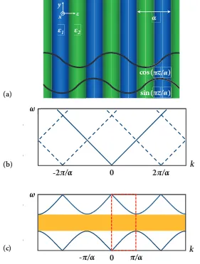
For a homogeneous dielectric medium with constant , to which an arbitrary artificial periodicity with period is assigned, the dispersion relation is simply (k) = ck/√ , as depicted in Fig. 2.1b. The assumed periodicity implies that the dispersion relation will repeat itself at = k+2m // , as shown by the dashed lines, leading to the crossing of the dispersion curves at k = ±m // . The aforementioned fact is simply the graphic representation of the existence in the periodic medium of two modes with frequency = cc // , that can be expressed as ± / or alternatively in the linear combinations f(z) = cos(( z// ) and g(z) = sin(( z// ) (Fig. 2.1a). Due to
23
cos( zz ) sin( zz )
1 2
z y x
k
0
-2
2
[image:38.612.153.434.82.454.2]
Figure 2.1 (a) Medium with one-dimensional periodicity in the z-direction. The high dielectric constant
regions (1) are shown in blue and the low ones (2) are shown in green. The distribution of the two possible
modes at k = ± // is depicted by the black curves. The mode with lower frequency low tends to concentrate
its energy in the high regions, while the one with higher frequency high concentrates its energy in the low
regions. (b) Dispersion relation ( -k) for propagation in the z-direction of a homogenous medium (solid lines). The assumed arbitrary periodicity leads to the periodic repetition of the dispersion curves at k+2m // (dashed lines). (c) Band diagram (dispersion relation) for propagation in the direction of a z-periodic medium. A photonic band gap (frequency region marked in yellow) arises due to the appearance of two modes with different frequencies ( highand low) at the same k = ±m // . The dashed red lines
indicate the irreducible Brillouin zone.
the homogeneity of the medium (in terms of dielectric constant ), the two modes have the exact
In a multilayer medium with periodicity a, in which the dielectric constant is actually perturbed according to (z) = 1+ cos(2 z/a), the two modes described above
anymore. More specifically, the same structure can in this case accommodate light of two different frequencies at the same k-vector, which simply means that there are two frequencies
highand low, with high > low that correspond to the two modes.However, there are only two
0
-
k
(a)
(b)
24
possible ways that the modes can be placed in the medium, due to the translational symmetry that is imposed by the periodicity: as Fig. 2.1a shows, the extrema of the modes can be located in either the low- or in the high- regions. In other words, one of the two types of modes (typically the one with low frequency low) tends to concentrate its energy in the high index material, while
the other (with frequency lhigh) concentrates its energy in the low index material. As a result,
there is a finite frequency range for which there is no allowed energy distribution (i.e. kzhas a
non-zero imaginary part there are no supported propagating modes) in the multilayer medium (Fig. 2.1c). The described behaviour is mathematically related to the solution of Schrö
equation in a periodic potential2, thus the forbidden-frequency zone is known as the photonic
band gap3. Effectively, 1D periodic media function as reflectors for the frequencies inside the
banb gap (and are also known as Bragg reflectors, due to the dependence of their reflective properties to the Bragg effect). The of the photonic band gap increases with the dielectric constant/refractive index contrast between the (two) materials of the multilayer medium.
The dispersion relation of photonic crystal structures is commonly referred to as the band diagram or the band structure and is the most important tool for their description. The band structure describes crystals in k-space (which is the spatial Fourier transform of the considered real space crystalline topology), as that makes the classification of the properties of crystals easier. In a band diagram the region k = ± // also known as the first Brillouin zone can be identified to be replicated periodically with period k =2 // . As k repeats itself outside the Brillouin zone, the higher order replications of the dispersion curve (observed at k = ±m // ) can be thought of as the curve of the first zone being folded back into the zone when it reaches
4. Additionally, as the curves have mirror symmetry about k = 0, the first Brillouin
zone can be further reduced to the region 0 < k < // , known as the irreducible Brillouin zone (indicated in Fig. 2.1c). It is apparent therefore, that for the study of any reciprocal periodic medium it is sufficient to consider only the irreducible Brillouin zone.
2.2.2 Two-Dimensional Photonic Crystals
Further to 1D Photonic Crystals (PhC), another type of periodic structure that can be commonly found in planar integrated photonic circuits are two-dimensional Photonic Crystals lattices. The
-periodicity in the xy-plane is assumed) and homogeneous along its third axis (here, the z-axis). The response of a 2D photonic crystal to an optical field varies depending on how the field is Fields in a 2D PhC, can be identified as: Transverse Magnetic (TM), for which the electric field is normal to the plane of periodicity, and Transverse Electric (TE), for which the electric field lies on the plane of periodicity.
25
0 0.1 0.2 0.3 0.4 0.5
M K
K M
TE modes
TM modes
Figure 2.2 Band structure of a two-dimensional triangular lattice of air holes ( = 1) of radius r = 0.28 on
a membrane Silicon slab ( = 12.11) of thickness 0.5a. TE modes are shown in blue and TM modes are shown in red. The inset shows the unit cell of the photonic crystal lattice (white corresponds to the air holes and green to Silicon), along with its reciprocal space unit cell (a hexagon rotated by 30o with respect to the
photonic crystal unit cell). The band structure was calculated for the wave-vectors within the irreducible Brillouin zone, formed by the central point of the Brillouin zone, and the two high-symmetry points M and K (marked in blue). A photonic band gap exists only for the TE modes and is marked in yellow.
lattice differently, the response of the system will be different in each case. In order to better understand that, the band diagram of a triangular lattice for both TE and TM polarizations is shown in Fig. 2.2. The structure under consideration is a 2D triangular lattice of air holes of radius r = 0.28 , in a Silicon (n = 3.48) membrane slab with thickness 0.5 , with the period of the lattice. It can be seen that a complete photonic band gap is achieved only for the TE polarization (blue curves) in the frequency range 0.255 < // < 0.301, while there is no band gap for the TM polarization. That is due to the fact that the oscillating optical field in each polarization case experiences the perturbation of the dielectric constant of the medium differently.
As the band diagram describes the crystal in k-space, the Brillouin zone is the spatial Fourier transform of the unit cell of the considered lattice. In this case, due to the six-fold symmetry for the triangular lattice, the (hexagonal) Brillouin zone is also six-fold symmetric, with two high-symmetry points that repeat six times. These two points, typically referred to as K and M, together with the centre of the Brillouin zone -point, define the irreducible Brillouin zone (marked with blue in Fig. 2.2). Here the band structure has been calculated only for the wave-vectors that lie inside the irreducible Brillouin zone, i.e. in the - - - region, as it has been explained that that is sufficient for the study of the band diagram of a photonic crystal.
It can be noticed that the lattice vector G, which as seen in Section 2.2.1 is given by G = 2 // , has a different length in different directions ( - -M and the directions in between).
Freq
u
en
cy
26
For the case of the triangular lattice considered as an example here, G = 2 /√3 in the -M direction and G = 4 /3 in the -K direction. That simply means that a 2D lattice has different periodicity in different directions. It is therefore important to consider the vectorial nature of k, as the angle of incidence and propagation of light in a 2D photonic crystal affects the periodicity that it experiences. Analogously, a 2D photonic crystal can be thought of as an omnidirectional superposition of 1D photonic crystals (i.e. Bragg reflectors) with a given periodicity. Under that consideration, it is understandable that crystal lattice configurations with as many symmetry axes as possible are desirable for homogeneous omnidirectional reflectivity (i.e. homogenous response for every k). As an indicative example, it can be mentioned that the triangular lattice configuration is considered superior to and is preferred over the square lattice one for two-dimensional photonic crystals, as its hexagonal reciprocal unit cell has a higher rotation symmetry than the square reciprocal unit cell of the square lattice.
2.3 Photonic Crystal Cavities
The understanding of the analogy between photonic crystals and crystalline materials led to the study and observation of many interesting phenomena. One of the most significant observations was the possibility of the existence of localized modes inside the band gap of a photonic crystal lattice [23], [24]: a defect in the lattice structure of a crystalline material can lead to the exhibition of new energy states inside the electronic band gap. Analogously, a perturbation of one or more sites of the lattice of a photonic crystal can result in the appearance of a single localized mode or a set of closely spaced modes with frequency inside the photonic band gap. These modes are
perturbation lies physically.
The above described system can be conceptually thought of as a resonator: the propagation of light in the rest of the photonic crystal is forbidden as the boundaries of the defect act as Bragg reflectors in the direction of propagation5. Therefore, light at the considered
(resonant) frequency oscillates inside the defect and only decays exponentially out of it (in the photonic crystal lattice) it is apparent that the defect acts effectively as an optical cavity.
Fig. 2.3a shows a photonic crystal cavity formed by removing the central rod of an ideal 2D
square lattice of Silicon rods in air. The appearance of a localized mode (represented by the green line) with frequency inside the photonic band gap for the TM polarization6 can be seen in the
band diagram of Fig. 2.3b. This is a convenient way of visually depicting the fact that the optical mode is confined in a photonic crystal cavity as a result of the omnidirectional photonic band gap (i.e. Bragg reflection) that it experiences about the perturbed sites.
5 Since it was assumed that the frequency of the considered mode lies inside the band gap of the photonic
crystal.
6 The structure under consideration exhibits a complete photonic bandgap for the TM polarization as the
27
0.2 0.25 0.3 0.35 0.4 0.45
F
re
q
uenc
y
c
Figure 2.3 (a) Point defect photonic crystal cavity formed by removing the central site of an ideal square
lattice of Silicon rods ( = 12.11) in air ( = 1). (b) Localized mode (green line) with frequency in the TM photonic band gap due to the perturbation of the photonic crystal lattice.
As for any optical cavity, there are two fundamental features that are necessary for the characterization of photonic crystal cavities: the volume of the mode V and the quality factor. The modal volume describes the spatial extent and the energy density of an optical mode inside a cavity. The quality factor (typically referred to as the Q-factor) is defined as the ratio of the energy stored in the cavity to the energy lost per optical cycle7 and expresses quantitatively how
strongly a mode is confined inside a cavity. Optical cavities with high Q-factor and small modal volume are a typical tool for achieving enhanced light-matter interaction. Owing to the exhibition of the photonic band gap that is equivalent to very high frequency-dependent reflectivity photonic crystal cavities can exhibit extremely small mode volumes (on the order of a cubic wavelength) with very high quality factors. For example, by removing a single site of an ideal photonic crystal lattice (corresponding to a band gap-wavelength sized modal volume), a cavity is formed with theoretically infinite quality factor.
For two-dimensional photonic crystal cavities in reality, where the lattice does not extend infinitely out of the plane (of periodicity), vertical confinement is achieved via total internal reflection. For example, in the case of a PhC cavity on a 2D slab (xy-plane) that is suspended in a medium with refractive index nsus, the confinement of the cavity mode is only possible if the
vertical component of its wave-vector (⃗ ) is imaginary (lossy) out of the slab. According to as
> ⇔ + > (2.4)
Similar - 8 (Fig. 2.4a) that represents schematically the total internal reflection
condition for simple waveguides, the schematic representation of the condition of Eq. 2.4 in two
7 Typically the quality factor of a cavity Q is related to the energy decay rate of the cavity through
Q = 0/2 , where 0 is the frequency of the cavity mode (i.e. a resonance frequency of the cavity).
8 - /k = c
0/nmat) in a material with refractive index nmat.
It is a useful tool to distinguish between guided and non-guided modes in dielectric slab waveguides, where the light-lines of the core and the cladding materials can divide the dispersion diagram into a region of discrete guided modes, a region of a non-guided mode continuum, and a forbidden region with no propagating modes.
![Figure 1.3 (a) Illustration of the cross-section of InGaAsP/Silicon hybrid laser based on metal bonding with excess material removal (image reproduced from [59], © 2011 IEEE)](https://thumb-us.123doks.com/thumbv2/123dok_us/8737299.387791/22.612.154.489.400.624/figure-illustration-section-ingaasp-silicon-material-removal-reproduced.webp)


![Figure 3.8 Monte Carlo simulations of electron scattering in photoresist (PMMA) on Silicon for electron beam lithography at (a) 10 kV and (b) 20 kV (reproduced from [4], with the permission of AIP Publishing, © 1975)](https://thumb-us.123doks.com/thumbv2/123dok_us/8737299.387791/71.612.221.394.298.440/simulations-electron-scattering-photoresist-lithography-reproduced-permission-publishing.webp)
