00
~~VXUTi
op
AIR UNIVERSITY
UNITED STATES AIR FORCE
I
/
SCHOOL OF ENGINEERiNG
INFORMATION SERVICEPropo tiru 'l fc ommbyc
II S, [ieJarlme,,q €,f Cv,,,~ee, .
*•igfiv',l VA 221,11
WRIGHT-PATTERSON AIR FORCE BASE, OHIO
D C
DOCUMENT CONTROL DATA.- R & D
sr. -untr ctas Wfaa.r , of tftfe. f-t .. t4 Ah-tvrc anJ rnd-.on: .u- ý nfatafjn r~nu.r #.c ývrv whent, he overji re.port is ci.,ssiflrda
I ORIGIdA TING AC TIV.YV 1C~npvrale allthor) G2.RLPOAT SECUMeT,
CLASSIFICATION--Air F.orce- Institute, ofL Taci-noloy (A.FIT--1)
LUnclas s i ied
) .;i~h-i~-* rs o te i o4 5Q103 1b. GROvP
3. REOTTITLE
laboratory Coviv-rsicn1 na Statc Descriptior
of the
D-17F. Com~puter
4. DESCRIPTIVE &TEfyotpvadcut-darts)
1`FIT' Tnsir
S. AU TH4Ofte fFuses nam~e. a,,dtfi instial. loaf fidme)
tDouflas J1. Alicn
6. REPORT *ATE AL. TOTAL NO0. C#F PAGES 7?&. No. OF revs
Jvne
1972
121
I
17
6.CONTRACT OR G0%AtT %0O 6. ORIGINIATOR'$ REPORT NUMDERISI
6. PROJECT NO.
;A2-C. 6.OTHER REPORT NOISI (Any ofihetnumbeis Met may be essigned
dt
SO. STRIOUl . STATEULZT
ITi~is
docua.-it Las been approved for public release and sale;
its dist rilbation is valir-it: d
A~Iprov-aorx'blic
release;
JA-W
AFR 11
(Y-10PNSYING LMILITARV ACTIVITY-.AAr . *. Force Logistics Comm~and
Keith A. Williams, 1st It., USAF
Acting Director of Information
I__________________
ID e7%CTLe
0-173
co:-.put.?r is
P
di~.itl rninicomipruter thit is use4 in
tle
:1I
i:nutc!Ž?ri"
I
missileiv -u.3-nce
system.;:
This
systct: 1,.-
teen
aac.-,-ic'!~n- tl... porc-...urcs
f:convr-!t_1nr
tha
cormut
lcrfor
:e'
rA;,l
rliurpo-
t-sc is L-An,.
~(:,v;:rzstf~d
'.y L.r.e I-.inutuct!2r Corinuter Lsers' Group.
This r-:!o-t .-
IS a:Jr:-s- ad tm.w-irz T'1t or tLat offort.
Vcor
te
convc-rsion .:-rcccss ;.s :o0run1 thre cc-ralter may bc
tczýtt:o to fut z.. 'Iev m
u
-lity.
:x1n~
'
f-orcced-air coo..int
*Wn:Crntary . sari~U~
L
Oý
O thb!
D-171, prmvzously anviiable
nic:
t.
~
~
,Y auL-pto[U ti.c st!3tus ofccnx:rol fliý3-!f2.-s.
-.;is st3ýtj zercri tin
is usz fj.lj ns a stuz~y
'n1-n nn n nintenarsc-_
t
%SuE,._-stions of educational applIerntions
P
-ja ta
1n:;ut
bi~s orz
inccimL~ccr
*ý.is ti
es is ca:1
--
Ovi-,-t2
ilior:ý.-jiwi m:cý!ssry tc c,:vvert ti c :)_171. to0 a lat.oratciry co-:uter
rr'itcuflt:ins
jniit
for
tlfore
in
46rest.-adin sirtil*,r
z.onversion'ýrojects.
I
LABORATORY CONVERSIO. AN)D
STATE DESCRIPTION OF THE
D-17B COMPUTER
Thlesis
G,
.,E
.!
-,
,,-
D
D C
Wou_"a J. Allen
Captain USAF
Approved for public release:. i"
distributiors udimited. IL
U
KEY WOROS -IN
- -I a
-IROLE 0? ROLE O? ROLE WT
l:inutem- n I Contuter
D-17i3 CoL-nuter
Co'nouter Conversion
GEIEE/72S-2
0
LABORATORY CONVERSION AND
STATE DESCRIPTION OF
THE D-17B COMPUFER
THESIS
Prese ted to the Faculty of the School of Engineering
of the Air Force Iissitute of Technology
Air University
in Partial Fulfillmen of the
0•
Requirements for the Degree oflaster oi Scienc
by
Douglas J. Allen. BS.E.E.
Captain USAF
Graduate Electrical Engineering
June 1972
Approved for public release; distribution unlimited.
-GF/EE/7-2S-2
0
I have always iAmired thosc 1vople who could ing-eniously find a new use for obsolete
equip-ment. When I .vas given
the
opportunity to be part of the effort to rcuse a computer, I was delighted.This report is the remit of my efforts toward the goal of providing documentation about the D-17B
computer and the procet.ure needed to change it from a missile control computer to a laboratory
computer.
I would like to thank Dr. Gay B. Lamont and Dr. Frank M. Brown for their tireless efforts
in advising the Minutema i computer project. Also, I wish to express my gratitude to Mr. Robert L
Mitchell and to Wr. Dale Wells. systems engineers at Newark Air Force Station. for their technical
assistance and for data that they so wiilingly provided. My sincere appreciation is due Mr. Robert G.
Durham for technical help and the AFIT workshop for their excellent craftsmanship.
A special thank you is due my wife and family fo. their patience, encouragement and
assistance in prepariing this report.
0
Douglas J. Allen
GE/vE/72S.2
Contents
0
Pg
Listeofa- . . ...
List of Frablas .. A... ,i
~
2 Ptesent;ttion of Problem Solutions-. . ... 2... 3
Funetion .. .scripion... ... 3
Bask Coir--,weivn!5 nd Termn, 4ology of the D- 17B---... 3
Control Undi
.... ..9
Afithi P.o.le. . 10...
I
MeSmorym~--- 12... ...
18
Comyiuto Wo-rd
F2o...
... ... 2S'alic Nuimber
n...3
Split Number ornt... 3
Sut scriona•eof ... 23
Non-Ctmoput States
- -.-25
9- Sarthe .stip ,tit_ 59 Other Techniques of Drbi. the ... 59VOutphuDiagram
....
60
Il. ntil rputl o rd Fof mt Ow.. 1..8... ... 6
hPmrrtion for Power 63 Fretat JWie I~kstpinsof the D-17B... ... Dfnin... .a. ... . ation y... ... ... Ascminliot s .. ... Nonclnur to ofEt erai l ... tor.. ... .6
Covrino Staans ... isl
~fs
oaComputer ... ... 566K-tSaeD-ci
lo
tm
a.
... ... ... .... 5
GEEE/72S.2
Contents
0
pap
Initial Pwer On h 67
Ecteimal Power Supply. ... 67
initi.i Power Application ... 67
Prepara ion of Cooling S 69 Coth'n:g System Gzncral Description ... 69
Mo~.ication of Computer Base ... 69
Memry Bl.'r. ... . ... ... 72
TMest
BsowerNCn
... ... 72Cornput, r Chieckout ... 74
Tests Using No Control Pal ... 74
Systcm Clock W o74 Tests Using Control Panel... 74
Bit C unterWa-efom... 76
Thrui g
Flip-flopWaveforms.
... ... 76Loop Waveforms ... ... 76
Summnary ... 76
IV. Applications of the D-17B Computer... . ... ... 81
General Purpose Input Bus
System...
. ...81
Educational Uses of the D-17B ... 81
Laboratory Uses of the D-17. ... 81
Data Collection Capabilities of the D-17B
.8.3..
...83
Summary-_ .83 ___
SC').
. V. Conclusions and Recommendations..- ... ... 84Bibliography .- - --- $55.. Appendix A: List of Terms and
Abbreviations
... 87Appendix B: Construction and Calibration of Temperature.Sensing Equipmentc... 91
Appcndix C: D-178 Wiring List-... 94
Vita . . 114
GEIEE72S-2
List of Fixures
C)
FigureI
Functional Block Diagram ofD-17
B Computer .... 62 D-17B Ward F7rmat
..
3 Typical r.17B Rx'circulating Register --- -...8
4 Veitch for Op Code Storage Register. ec ... 1I 6 D-17B Bityaotr ... 13
6 D-17B ,Memory Laob.14 7 D-178 Cot tputer Word
Forests
... 248 D-17B Not.Compute State% - - 28
9 D-17B Noc4tompute Fill-Verify States.. ... 29
10 D-1711 Compute States...34
11 X-Special Compute States .. 35
12 Y.Special Compute S tat.. ... 36
13 D-17B Discrete Outputs ...--... 56
14 Veitch Diagra-n of Compute Mode... 61
IS Veitch Diagram of Nontompute Mode... 62
16 Location System Used in CI.zckout Procedures of the D-17B... 65
17 D-17B Memory Power Supply Waveform ... .... 68
18 D-171 Computer Temperature vs. Ambient Asr Temperature ... 70
19 Air Exhaust Modifications on D-17B Computer Suppoxting Framc... 71
20 D-17B Cooling System Using Electronic Equipment Rack Blower ... 73
21 D-17B Cooling System Using Two 6-inch Fans... 73
22 D.17B System Clecd. Waveform.,
75
23 D-17B Bit Counter, B1. Wvform ...- 7724 D-17B Bit Counter, B6, Waveform ... 78
25 Tp Timing Pulse 79 26 Lx Flip4lop Output W---... 80
"27
D-17B Input Bus BlockDiagam...
8228 Temperature Sensing Equipnts... .... 90
=v
_)
2_-GE/EE/72S-27
List of Tables
o
Table
PUP
I
General Spidfications
of the D-17BComputer...
...4
U1 D-17B Co, iputer DC Power Supplies, Voltages, and Tolerances... ... S
III D-!TB Com puter Input octos... 16
IV Character a ,put Codes for the D719
V D-17B Ccm.puter Output Pin Connections ..._ 20
VI D-17D Digiial-to-Analog Voltage Output Locations...____ _ _ 21
VII Register Tiansfer Notation Used in tie State Description of the D-17B
Computer ..- - 26
VIII Register Tr msfer Equations for Noncompute States of D-17B Computer... 30
IX Register Transfer Equations for Compute States of the D-17B Computer-- 37
X [ogic Equations Used in a State Description of the D.17B Computer-... 44
0
rr ,
I.I
i G•EIEEI7S.2
0
The D-17B coirputer is a digital minicomputer that is used in the NSQ.10 Minuteman I
missile guidance system. This system has been made available for reutilization by qualifying
agencies. Documentatior concerning the procedures to convert the computer for general purpose
use is being generated by the Minuteman Computer Users' Group. This report is addressed toward
part of that effort.
Before the conversion process is begun the computer may be tested to determine aseability.
An inexpensive forced.air cooling system will allow operation at ambient air temperatures up to
850F. Fragmentary descriptions of the D-17B previously available are supplemented in this report
by a description using the states of control flip-flops. This state description is useful as a study
plan and a maintenance guide. Suggestions of educational applications and a data input bus are
in-cluded. This thesis can provide the information nectisary to convert !he D-17B to a laboratory
computer and it contains data for those interested in similar conversion projects.
GEIEE/72S-2
L. ntroducfiinn
(-1.)
This thesis was undertaken to investigate the conversion of the Minuteman I guidance computer to a general purpose laboratory computer and to provide a state description of the computer. Inorder to discuss this prcolem in more detail. it is necessary to consider the background of this problem
and some general definitions of computer classes.
Backround
The modeiniwai m of the Minuteman Intercontinental Ballistic Missile Force has made it
inecessary for the United States Air Force to declare over 1,000 outdated inertial guidance systems
unserviceable. Each oft tese model NS-IOQ guidance systems contains a D-17B computer, pow"r
supplies, and the unclassiied parts of the stable platform.
These systems ae available, for only the shipping costs, to colleges and other qualifying
organizations. Unfortunately, written procedures for reutilizing the system were nonexistent and
only fragmentary c.-scriptions of the machine were available. Thus, this effort met an early impasse
because of the lack of documentation concerning the D-17B.
The Minuteman Computer Users' Group (MCUG) was formed by Dr. Charles Beck at Tulane
University for the purpose of consolidating the efforts of potential usc;s of the D-17B. It is intended
that the members of this cooperative may share the r':slts of their research and overcome the initial
reutilization problems (Ref 7:ii). The Air Force Institute of Technology (AFIT) is a member of the
MCUG and it is hoped that this report will be used as part of that effort.
AFIT obtained two NS-10Q Minuteman I guidance systems in June 1971. Since that time,
four thesis pr jects have been undertaken as part of an overall plan to convert a D-17B computer
from one of these NS-IOQ systems into a useful laboratory computer. One of thewe projects (Ref 8)
deveoped a control console for the computer. Another project (Ref 13) developed an input/output
interface, and a third effort (Ref 9) produced a software simulation for the D-17B. The fourth thesis
project is the subject of this report and its purpose and plan of development will be explained in the
following paragraph.
Deffmitkins and Problem Anal-sis
In order to accurately describe the unmc 5-fied D-17B computer and the planned modifi.
cations, it is n,6cessary to define a general-purpose and special-purpose computer. A general-purpose
computer is a computer designed to solve a wide vatiety of problems. In contrast, a special-purpose
computer is desipiizd to solve a specific problem or a restricted class of problems (Ref 4:202). The
GEIEE/72S-2
lines of a general-purpo c. computer, but when used as part of the Minuteman System it functions as
a special-purpose machine.
Essentially thor .the problem involves changing a special.purpose compu!er to a
general-purpose computer. T"][C extent and type of modifications depend upon the following assumptions.
Assumpt i10 ( omputers similar to the D-I 7B arc commercially available for ltss than
SIOWO0. It can be ase r-ned thut future us,;rs of the D-17B will require minimal conversion
expendi-tures; otherwise, it woulN be advantageous to purchase a new machine. It is also necessary to assume
that the computer and -- sociated power supplies would be uscd in their present physical package,
which is a right circular ,.ylinder, 29 inches in diameter and 20 inches high. These dimensions could
be reduced by iepackagir g the comlputer. but the cost of such a modification would be prohibitive.
It is assumed fth t the modified computer will be operatetd in a laboratory where the
temp-erature of the rbom can be controlled within the range of 65-850F. This assumption provides a
standard for designing a new cooling system for the computer.
Subproblems. Since the computer was cooled. in its original confsuration by
special equipment associated with the Minuteman Missile. a new cooling system must
be designed. This design will be under strict economic limitations and should be as
r
('sifsple as possible
In order to operate the D-i7B computer, the user must know how the machine
functions. A major subproblem of this thesis will be to describe the computer in several
ways so that each user may choose a description that best suits his application.
A third subproblem will be to develop procedures that will allow future users
to determine the operational status of their particular D-17B. These procedures are
desirable since they give the user the assurance of knowing that the computer will
operate, prior t1 beginning the conversion process. "
Presentatior. of Problem Sohttions
Chapter 1i of this repot. presents five different types of descriptions of the D-17B: A
physical description, a functional description. a description or the word format, state descriptions
and mode description. Chipter Ill discusses the initiL. preparation. checkotet. and a cooling system
for the computer, and is written for the technician who is faced with installing the D-17B in the
laboratory. Chapter IV briefly di.euws some applications of !he D-17B. and Chapter V presents
GE/EE/72S-2
II. Descriptions of D-1 78 Computer
In this portion of the report the D-178 computer will be described from five
basic points of view. fhese descriptions range from a general overview to a specific
analysis. First, a bas;w physical description will be presented; second, the computer will
be described in terms of five function.l sections; third, the word format and information
necessary for programrlin- Vtill be brietly discussed; fourth, register transfer will be
described using state d.agram techniques: and, finally, some alternate descriptive techniques
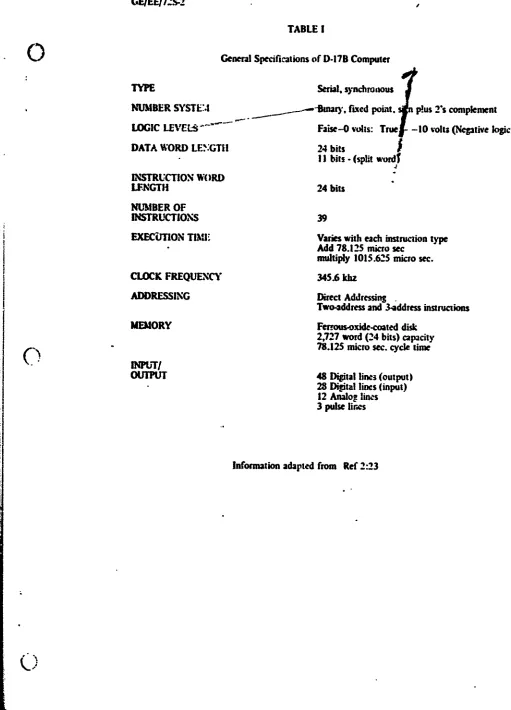
will be covered. General specification' of the computer are listed in Table i.
Physical Description
Size and Comp isition. The D-17B computer occupies one-half of a right
polygonal-cylindrical shell. This twelve-sided cylinder is 20 inches high, has a maximum
radius of 29 inches and the shell is 6 inches in depth. A power-supply for the complete
NS-IOQ guidance system is contained in the remainder of the shell. A stable platform.
the third major item of the NS-10Q, occupies the cavity formed by the computer and
power supplies.
- The computer alone weighs 62 pounds and is composed of 76 printed circuits
and a rotating disk memory (Ref 14:16).
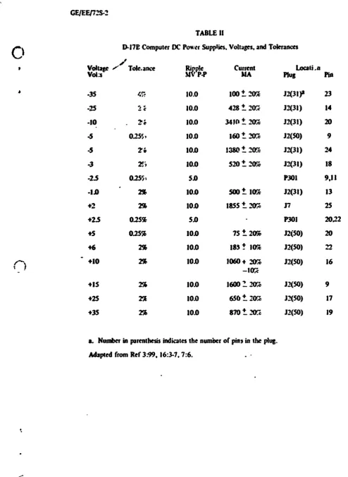
Power Requirements. If the associated power supply is used %ith the D-17B, it is necessary
to provide 28 VDC, 19-25 amps from an ecternal source. The computer may be operated without
the accompanying power supply; however, it is necessary to suppLy fourteen separw!e DC voltages
as well as 12.00 and 400 hz alternating current supp.ies. These secondary power specifications are
listed in Table !1. Power consumption for the computer alene is approximately 350 watts (Ref 11:16).
Functional Description
"The
D.i7B •.y be divided into five basic functional parts: the Control Unit. Arithmetic Unit, Memory. Input. -nd Output. This division is shown in Figure I (Ref I i:TR24).Basic Components and Terminologv of the D-17B. Each functional section of the D-17B is
composed of basic components o! building blocks that are common to several parts of the computer.
These components must be described and common tetminologey must be defined in order to adequately
describe the funtionmd parts of the computer.
The term bit will be used as a shortened form of binary digit. Thus. a bit of information may
be stored in a two-state dcarcc such asa :lip-;1lop. An exitcnmin of this notion ead& tit an ordered set
GE/EE/7:S.2
TABLE I
0
General Specifications of D-17B ComputerTYPE Serial, synchronous
NUMBER SYSTE'.I *-Bmazy, fixed point. s Pn lus 27s complement
Ig
LOGIC .EVEL•..' Faise-0 volts: True- -10 volts (Negative logic)
DATA WORD LENGTH 24 bits
I
I I bits - (split wordl
INSTRUCTION WORD
LFNGTH 24 bits
NUMBER OF
INSTRUCTIONS 39
EXECuTION TIM!I Varies with each instruction type
Add 78.125 micro sec
multiply 1015.625 micro sec.
CLOCK FREQUENCY 345.6 khz
1ADDRESSING
Direct AddressingTwo-address and 3-address instructions
MEMORY Ferrous-oxide-coated disk
2,727 word (24 bits) capacity 78.125 micro sec. cycle time
OUTPUT 48 Digital lines (output)
28 Digital lines (input) 12 Analog lines 3 pulse liracs
Information adapted from Ref 2.23
I4
[image:15.630.35.546.58.768.2]GE/EEI72S-2
TABLE If
D-171 Computer DC Power Supplies. Voltages, and Tolerances
Voltage .'Tole~ance Ripc Current Locati .n
"Vos
M? P.P MA Plug Pin.35 47 10.0 100t -_M J2(31)2 23
-25 !10.0 428.t02 J2(31) 14
-10 Z; 10.0 341o t 20% J2(31) 20
-5 0.255) 10.0 160 t -' J2(50) 9
-5 2'? 10.0 1380. 20% J2(31) 24
-3 25 10.0 520 4.20% J2(31) 18
-2.5 0.255- 5.0 P301 9,11
-1.0 2% 10.0 5004.10% J2(31) 13
+2 2% 10.0 1855 t. 22 V7 25
+2.5 0.25% 5.0 P301 20.22
+5 0.25% I0 75 t 20% J2(50) 20
+6 2% I0.0 185 t 10% J2(50) 22
+10 2% 10.0 1060 + 20n J2(50) 16
_ -10%
+15 2% 10.0 1600 I 20M J2(50) 9
+25 2% 10.0 650o. 20t 32(50) 17
.35 2% 10.0 870 t 2M. J2(50) 19
a. Number in parenthesis indicates the numoer of pins in the plug.
[image:16.645.55.550.58.736.2]Gi/.42./725 -2
nw LI
1%W
*1
a
w
z0
wsw
z
2
~
*rO 0:U.S
lz 8W
w to
GE/EE/72S-2
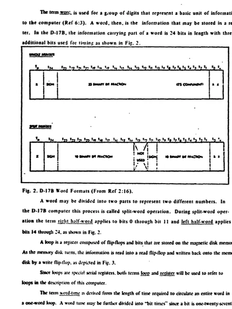
The term QxoL is used for a gloup of digits that represent a basic unit of information
("
to the computer (Ref 6:3). A word, then. is the information that may be stored in aregis-ter. In the D-17B, the information carrying part of a word is 24 bits in length with three
additional bits used for timing as shown in Fig. 2.
to .1'a 124 '23 ] ,T r?"1i r~. 1' t l t o Tlol I-* '1 It Irs I? h, IslIs 1a 3 1' I LL to 1
Ia
I
W.i W•.Mo,3 M II
0
-jSin
m n n ...Fig. 2. D-17B Word Formats (From Ref 2:16).
A word may be divided into two parts to represent two different numbers. In
the D-17B computer this process is called split-word operation. During split-word
oper-ation the term right half-word applies to bits 0 through bit 11 and left half-word applies to
bits 14 through 24. as shown in Fig. 2.
A loop is a register composed of flip-flops and bits that are stored on the maintic disk memory.
As the memory disk turns. the information is read into a read flip-flop and written back onto the memory
disk by a write flip-tlop. as depiced in Fig. 3.
Sace loops. are s ccsrial registers. bote terms loop and rceister will be used to refer to
loops in the description of this c"omputer.
The term uord-timc is derived from the length of time required to circulate an entire word in
a one-word loop. A word time nuy be further dividcd into -bit 1im- since a bit is one-twenty-seventh
of a word.
The bits in a *otd nxyi be coded to form an instructkin for the computer. Diffcrent parts of
"the
word may be do-ld t ni.s ., '.x:alc unfout:ution si-h .is the "-dJrcLs7 t nlor eo.y hkxito'ais to [image:18.645.129.586.76.684.2]GE/EE172s.2
a00
[image:19.645.85.581.76.698.2]GEIEEI72S-2
a field. Fields are also commonly used ta indicate what operation iL to be performed (Op Code) or
what addresses of numbers are to be used in the operation (operand). This leads to a method of
dacsifying instruction words- by the number of addresses in the ins. action (Ref 10:452).
Control Unit. The primary fun-Ltion of the Control Unit is to interpret machine instructions
and direct the execution of these instructions. Therefore, the Instruction Regiter (1) is one of the
major components in the Control Unit (Ref 11:16).
The I.ioop'or Instruction Register is composed of one delay flip-flop, Ip, and a read and a
write flip-flop, Ix •-nd 124 respectively. Twenty-four other bits of th:s one word register are wjitten on
the disk memory. New information may be entered into the I loop when -he control flip-flop Ic
is "one" set; otherwise, the information circulates from the magnetic disk through the I flip-flop and is
re-witten on the disk in a continuous loop.
The I register receives the computer instruction from the memory and holds that instruction
for part of the instruction interpretation. Prior to execution, the instruction is read into various buffer
registers and the I register is free to reeive the next instruction to be executed (Ref 11:16).
The Operation Buffer Register is used to store the instruction operation code prior to execution
(see State Description 02). This register consists of flip-flops Ip, Ob3.0b2bl. During the last word time
,) of execution, the next instnrction is serially loaded into the Operation Buffer Register, then parailel-loaded
into the Operation Code Storae Register. Flip4-flps. 04,03,02, 01, form the Operation Code Storage
i.
Register which serves primanrl to hold the op code dtjring execution (see Word Format for an
explan-ation of the Op Code) (Ref 1 1:27).
Storage of the operand information is accomplished in a similar manner by the Channel Buffer
Register and the Channel Storage Register. During the Instruction Read operation, the operand channel
information is fed into the Channel Buffer Register. flip flops CbS through Cb I. When the oerand
sector is found (see memory for discussing sectors), the operand channel is parallel-loaded into the
Channel Storage Register. flip-flops C5 through CI. This register then holds the operand channel
in-formation during execution of the instruction. Some operatio.-s do not require an operand and the
Channel Storage flip-flops may be used as additional hardware to execute the instruction. An
ex-ample of this application is the Character Output operation: four bits of the Accumulator awe shifted
into the Channel Storage Register to be output to the cluracter output lines (Ref 2:TR-72).
aFlg Storing is a special operation, and it is explained in the word format description. In
this oporation th., penvious contents of the Accumulator atre stored in a channel specified by the
in-struction. A code for that channel number is !,nded into the Flag Code Buffer Register. Sb3, Sb2,
GE/EE/72S-2
parallcl-loaded into the Flag Code Storage Register (Ref I 1:TR45). A set of diagrams showing the
codes that may be loaded into these registers is displayed in Fig. 4.
When an operand is read from memery it is loaded into a rqeistcr of the Control Unit called
the Number Register. The Number Register or N-loop consists of tht-re flip-flops, Np, N24, N', and
twenty-four bits of memory. The thiec tlip-flips N1p. N24. and N :ire used for delay, writing on the
memory disk, and reading. respective~y. and a fourth flip-flop, Nc, cor trols the entry of new
infor-mation into the N-loop (Ref 11:31).
There are four Output Control registers which are a part of the control unit. The composition of
these registers will be discussed here, but their functional task will be discussed in the Output functional
description. The Discrete Output Register is contained in the Control Unit. It consists of five
flip-flops, D5 through DI, which, together with a Discrete Output Matrix, control the twenty-eight
Discrete Outputs. Digital-to-analog com-ersion control flip-flops form three registers of eight flip-flops each.
The registers are designated Vi, Výi, and V3i. i 2 !,°" -,S. The Binay Output Control Register
con-sists of three flip-flops: G3, G-,G 1.
Tuning control of the D-178 is achieved using a bit counter that is controlled by the sector
track of memory (see "Memory" for a discussion of the sector track). The bit counter is a set of
flops that are used to distinguish bit times of the serial operations of the computer. These
flip-flops awe designated B It B B3 B4. B5, B6. Tp, TX, To. Tp, Tx. and To are timing flip-flops that are
"one" set only at the beginning and ending of words (the use of these flip-flops is apparent in the Word
Format discussion). BI is used to di..mguish between odd and even bit times and B, is "one" set and
"zero" set at alternating two-word time periods. B3 is "one" set only during the right and left
split-word bit times. B4 and B5 are counting flip-flops that support the other flip-flops of the bit counter.
B6 is "zero" set during the fast half of the w.ord time and "one" set during the second half (Ref 11:25)
The reationship between the 8 1flip-flop and tlh word times is shown in Fig. 5.
These are the major components of the Control Unit. Interaction of this function and the
following functional units will be discussed in the State Descnption of the D-178.
"Arithmetic
Unit. As its name implies, the purp-se of the Arithmetic Unit is to perform the calculations as directed by the Control Unit. Each of these Arithmetic operations is explained in theState Descsiption. This unit consists of two one-word registers. the Accumulator and the Lower
Accum-ulator. (Ref 11:17)
The Accumui•tor holds the results of all arithmetic functions and is an output register for the
-"... voltage, binary, and dcraoter output operatkiot: (Ref 11:17). In addition to 23 bits on the magnetic
disk, it is composed of two delay thp-tlops. A p and A24, a write flip-flop. A23. and Ax. a read flip-flop.
0 33 10
I
I
fi
-So- I n 34 16 10
- C1
Fl~a" Code Duffer
n 6 2Register-
--30 34 4 a
v MM
*
04 - -C
SAO M SU MM SW
-Go
am
in
Qm
AMO SUS UAM~~~I-
-on0 4741 (20 1a
CIA P0 O SCJ
an) 51 0
Channel
Stora~ee I'egisterr
IA TIw'
OperatiLon Code Stor2ge
Re~ister
Fit.
If
eitch
Discrar. for Storn'e iierister C'odes
GE/EE72&-2
When the control flip-flc,.i, Ac is "zero" set, the A loop is allowed to circulate and new information
may be sermilly loaded ino the Accumulator when Ac is "one" set (Ref 11:30).
The Lower Accumnulator, L-loop, is used for rapid access storage, character inputs, and logical operations. It consists o. two delay flip-flops. Lx and Lp. one write flip-flop, L, a read flip-flop,
Lo. and twenty-tiaree bit. ,.n tho matinetic disk (Ref 11:31).
Memory. Memutry in the D-17B is a rotating rngnefic disk. Information is transferred to
the magnetic disk by stati ,nary read and write heads. This information remains on the disk until new
data is recorded. Therefor!, this information is in non-volatile storage; that is. the informationremains
stored even when power t removed from the computer. However, the loops may be considered as
volatile storage, because th, flip-flops that are part of the loop will be activated in a random state when
power is returned to the computer (Ref 11:17).
hi order to define specific locations in memory, the disk is divided into 128 radial divisions
(sectors) and 21 concentric tracks (channels) as shown in Fig. 6. The sectors are numbered octaHy
from 00 to 177 and channels are numbered in an even octal progression, 00.02. ---., 50. (Channels
are numbered evenly because the least 4gnificant d;.jt of the octal number used for channel addressing
is part of the sector address). The sector numbers are recorded on the memory in a special sector track.
S; however, these sectors are numbered one sector out of phase for timing purposes in the computer.
Each channel and sector number designate 27 bits (one word) of memory. Twenty of the channels
are called "cold storage channels" because the write heads on these channels may be deactivated
(Rdf 11: 17).
In addition to the part of memory defined by the sector and d-awnel divisions there are ten
recirculating loops, which are used in input, arithmetic, and rapid stora-ee operations. The A, L.N, and
I loops function as part of the Arithmetic and Control Units. Rapid access storage is provided by the
U-loop, which is a one-word registcr consisting of a read flipflop, Up, and a write flip-flop, U., and
twenty-five bits stored on the memory disk.
The F loop. a four.wordrapid access storage register.is comprised of Fp. a write flip-flop.
Fx, a read flip-flop, and 106 bits on the memory disk. Two other four-word loops, V and R, are used as input loops. The V loop contains a Vp and Vx flip-flop and the R loop uses a - ad Rt
flip-flop for write and read functions respectively.
Rapid access storage of eight words is provided by the F loop which is composed of a read
flip-flop. Ex. a write flip-flop. Ep. and 214 bits on the rotating disk. A read amplifier. E.. is provided
"at
the midpoint of this register to allow rt•pid accem to the E loop contents. The I1 loop is a 16-wordGEIEE/72S-2
- r1
0- -f. ft
4D T-- - " -' d
2 - -. --- - - O--- - -- 0-- 0 0- --- - --- - - - - -" 0
S0 0 - - - - - - - 0 0 a0 0 - - - - - - - 0 0 O00
Cd M d I ii .. . .
2 0 0 0 mm0 0.0 - - - - - - - - - --
2 0a 00 00 a0 a 00-
---Fit 5- D-7 i0outr(rm- :R
GE/EE/72S-2
0i
1 1 1
L;=j ld
A .I
d...D Z Z Z Z Z
GE/EE/72S-2
-apid access storage register. Like the other loops, the Hp and Ilx ilip-flops are used for writing and
)
treading from the memory disk. An intermediate read amplifier, tImx. is provided at the midpoint ofthis register to allow rapic access reading (Ref 11:34).
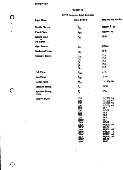
Inputs. In this report, inputs to the D-17B will be disc'sed in two general classes: control
input signals, and data inlputs. Control input signals are those signal; which would be generated by
a control panel or input d -vice to cause the computer to enter a piticular state or to accept data.
Data inputs are defined as character input signals and discrete input .ignals. Both classes of inputs,
associated common symbcis, and plug connections are listed in Table Ill. In the following discussion
of both control and data inputs, voltage ranges and general specificat.ons are given; however, these
ranges have not been completely test.d on the computer at AFIT. I is known from experiments that
these ranges are conservative and that successful operation has been rchieved outside the listed ranges.
These input voltage levels are adjusted by input circuits in the computer to obtain the level required
for machine operation. The adjusted signal is signified by adding a (*) to the standard symbol. thus
an adjusted fill signal woutd be Fs:.
Discrete Disable, Ddc, is a control input signal which deactivates the discrete output signals.
The "true" or "I" level is +10v with a worst-case current of 22 amps. Typical load is 135 milliamps.
Fake level is -25v with 4.0 microamp load (Ref 1:69).
The control signal Enable Write, Ewe, controls the write flip-flops in the memory "cold
storage" channels (0046). "True" for Ewe is +35 to +39v into a 120 ohm resistance connected to
-30v into a I meg ohm impedance (Ref 1:68).
Initiate load or Fill signal, Fsc, allows the computer to leave the Manual llalt states and enter
the Wait state. "True" or "'" for this signal is -16 to -30v into a 8.2k ohms resistance connected
to
+25v,
The "f:lse" level is+6
to +30v into a resistance ofI
meg ohm.The Mechanical Reader Input Signal, !m. is rot used in the control console at AFIT. It
may be used as one of several commands to enter the Wait state (see State Description). !m has the
"same
specification as the Fil! signal.The lalt prime or Run, K'hc, input aignal allows the computer to enter the compute states.
"True" for this signal is -16 to -30v into a 4.1 k ohm resistance connected to 25v and the "false"
level is +6 to +30v into I meg ohms (Ref 1:63).
"Ki
and Kir are both used as symbols for the halt or run prime signal. It is used to cause the computer to enter the non-compute states. Signal specifications are the same as Kilc (Ref 1:63).GEIEEI72S-2
TABLE III
0
D-17B Computer Input LocationsInput Name Inpui Symbol Plug and Pin Number
"Disable
Discrete Ddc Jl(100) a -23Enable Write Ewc . !(100) -93
Initiate Load Fsc 18-24
or
FaillSignal
Gyro Bottom lbc Ji0-22
Mechanica Input Imc J8-17
Character Inputs 1ic J7-1
12c .7-2
13c J7-3
'4c J74
15c J7-s
Ialt Prime K? .7-17
Run Prime Kir J8-16
Master Reset Mrc Jl(100) .90
-Sprocket Timing T€ J8-38
Sprocket Timing TC J7-6
Pr ime
Discrete Inputs XIC Jl(100) -96
X2C Jl(100) -97
X3C J3(10) .98
X4C J1(100) -99
XSC J9-7
X6C J10-23
X7C 39.2
X8C J9-3
x9c J9-4
XIOC 19-5
X iC J10-19
X_'_2C
J.1(100) .63
X13C
JIO-20
XI4C J3(106)48
Xi5C J1000) -18
X16C J3(100) -65 XI7C J3(100) .66
X18C 1l0-21
X9IC 19-10
[image:27.637.39.550.38.741.2]GEIEE/72S.2
TABIE III (cont)
0Input
Name Input Symbol Plug and Pin NumberDiscrete Inputs (ces.t) YIC J10 -1
Y2C JlO -2
Y3C JO -3
Y4C J1O .4
YSC
Jl(100) -95Y6C Jl(100) -94
YTC J3(100) -'76
Y8C J9-11
Y9C J9-12
YIOC J9-13
YI IC 39-14
YIVC J9-15
YI3C 39-16
Y14C J9.17
Y1SC J9.44
YI6C J9-45
YI7C 9.-46
YI8C J9-9
Y19C J3(0) -.29
Y20C J3(l00) -28
Y21C J3(100) -17
Y22C J3(100).16
Y23C J3(00) .6
Y24C J3(100) .5
GE/EE/72S-2
Master Reset. Mrc. is used to set the control flip-flop to a specified set of settings. Signal
()
specifications are similar to the Fill signal specifications.
The Sprocket "rting input signal, Tc, is an input which :auses the computer to accept
*data from the characte!r input lines. "True" level is -3 to .30v tald -false" is +20 to +30v. The
inverse signal is Tc, lacwever. Tc has the same signal specificatio.is; twe is -3 to .30v and false is
*20 to +30v.
Input signals lis ed in the above paragraphs are control inj uts. Next, the data inputs will
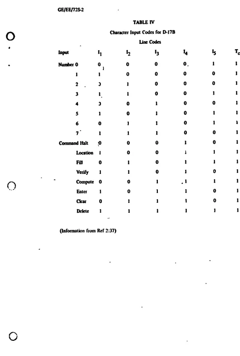
be specified. Character nput lines, li to 15c provide input :odes f r both command and numeric
data. These codes ate listed in Table IV. Signal specifications for -he Character Inputs are the same
as the Fill signal (Ref 1 :u2).
Discrete inputs Xlc - XI9a and Y Ic -Y24 are two sets of on.off type signals which may be
loaded directly into the Accumulator under program control. A special discrete signal input Ibc
is available and may be reset under program control. In the original configuration. this sigual was
used to indicate a gym malfunction. Signal level requirements for these signals ate the sa-nce as the
Fill signal (Ref 2:46).
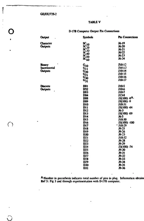
Outputs. Four types of output signals will be considered under this functional heading:
single ciaracter, binary, analog voltage, discrete outputs. Voltage limits and load limits are listed
(O)
with each of the outputs; however, these limits were extracted from Re-f 1:40-59 and were not testedas part of this report. Pin connections for these outputs are listed in Table V and Table VI.
Single characters may be output on output lines S.l through Sc4 Under program control
the four most significant bits of the Accumulator may be shifted to the lines for : pesiod up to
31 word-times as dictated by the program instruction. During the above period a timing signal
is supplied on output line Sct and eve.n. parity is indicated on line SoS "True' level for the
signals is -23.7v through a I k ohm resistor and maximum load is 50 milliamps. "False level is
+10.8v through 2 k ohm resistance for loads up to IA milliamps and +25v through a 12 k ohm
restance for loads above IA mifliamps. Maximum current from the circuit should be 4 nuilinmps.
Bitary Incremental Outputs were ,sed in controlling the navigational gyros. These outputs
are changed by the Binary Output instructions which cause one- of three flip-fhops to be set according
to the sign of the Accumulator. %hen the BOA instruction is executed. the CGI flip-flop is "one" set if the
Accumulator is negative and "zero" set if the Accumulator is positive. Output line GII is -true" if
G, is "one" set and line GIO is truc" if is -zero" set. Simibrly. the BOB instruction controls
outputs G,0 and G11 and the 0OC instruction controls the G3(and G3 1 output lines. "True"
for these outputs is -10, t1hrouith a 470 ohm resistance requiring load currents
less
than 15 milluamps.GEIE,/72S-2
TABLE IV
S
0
Character Input Codes for D-17BLine Codes
Input 1l 12 13 14 15 Te
*tNumber 0 0 0 0 0. 1 1
I 1 0 0 0 0 1
2 3 1 0 0 0 1
3 1 1 0 0 1 1
4 3 0 1 0 0 1
5 1 0 1 0 1 i
6 0 1 1 0 1 1
7 1 1 1 0 0 1
Command Halt 0 0 0 1 0 1
Location 1 0 0 1 1 1
Fill 0 1 0 1 1 1
Verify I 1 0 1 0 1
Compute 0 0 1 .1 1 1
"Enter
1 0 1 1 0 1CMar 0 1 1 1 0 1
Delete I I I ! 1 !
[image:30.630.57.545.46.769.2]GE/EE/72S-2
TABLE V
Q•
O D-17B Computer Output Fin Connections
Output Symbols Pin Connections
Character sciO J6-19
Outputs SC20 X620
SC30
J6-21
Sc•4
J6-22so J6-23
Sc6 0 J6-24
Binary 3l 10-12
Iceeu Gi J0-13
outputs G20 1JO-14
G21 Jl0 Is
G30 JIO-16J10-17
Discrete DO] j105
Outputs D02
JilO.6
D03 J10-7
D04 J13.8
DOB J3(l00)
)4A-D09 J3(10G) -9
D10 JIO-31
DI I J3(100) .64
D12 J6-3
D13 J3(100) -89
D14 J6-5
DIS JIO-30
DW6 J3(100) -i00
D17 MJ1029
DIg J9•25
D19 J9-26
D20 J9-23
D21 JI0-32
D22 J9-28
W23 J9-29
D24 J3(100) -74
D25 J9.30
D26 J9-31
D27 J9-32
D28 J9-33
D29 19.34
D30 J9-35
D31 J9-36
A-Numbte in parcntl-csis indicates total number of pins in plug. Information obtained from
Ref 5: Fig 3 and throug-h experimentation with D-17 computer.
[image:31.637.63.534.23.744.2]GEIEE/72S-2
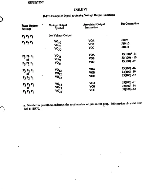
TABLE VI
0
O D-17B Computer Digital.to-Anal Voltage Ouitput LocationsPhase Register Voltage Output Associated Outpit Pin Connection
Settings Symbol Instruction
r3 r2 Pr No Voltage Output
P3 Pr2
r V01 0 VOAJIO-9
V020 VOB JiO-10
V030 VOC JlO-I I
..
r2V!vot
VOA
J3(100)P .21
or
V0
21VOB
J3(0oo). o
P3 r2 PI V03 1 VOC i3(100).19
r3 !2 pI
V0
12
VOA
J3(100) -46
or V02 2 Vol J3(100).59
P3 ?2 PI V03 2 VOC
i3(100)-52
r3
P2 P!
V0
13VOA
J3(1O0) .7'
or V02 3 VOB J3(1O0) -7
"P3 P2 Pl
V0
3 3voc
i30oo) .87
a. -Number in parenthesis indicates the total number of pins in the plug. Information obtained from
GEIEEI72S-2
"False" voltage level is -I v through 470 ohms with load curents I=ss than 30 milliamps.
0
Three separate digital to analog converters are available in the computer output networks.Voltage values are proportional to the split word contents of the Accumulator. The VOA instruction
causes the most significant bits of tlh, split word in A to be trasfe -fed to the Voltage Output
Register number 1. Flilp-flops in this regi'.ter direct plus and minus iv to eight different points in
a resistor network to prod ice an output voltage btween -I N0. 1f bit 14 is a -l". the tight half
of the Accumulator will b,' used for output, otherwise the left half-.ord will be used to specify the
voltage flip-flop settings. Similarly, the VOB and VOC instructions, ontrol output register V2i
and V3i (0l,
..
,). The twee voltage outputs may be directed to -ivy one of four sets of outputterminals depending on the Phase Register Contents. The setting Pý, iS2, Pj inhibits all voltage
outputs; other Phase Register settings and pin locations are shown in Table VI. Syrmbols for the
out-puts are VO. where i is either 1. 2, or 3 corresponding to the VOA. VOB. and VOC instruct ions
respectively. The second subscript, j. refers to one of the four Phase Register settings (Ref I !:TR70).
AJI of the outputs vary between 20v at a maximum load of 4 mila2mrs,
Twenty-eight discrete output lines are av-ailable and may be turned on and off under proi;.mt
control. Discrete line D04 is the only line that may be "on" while another disciete output is arl.
SIf D04 is on and DO,, '1)02, or D03, is turned, it will remain o0. In all other c.scs , if any
dis-crete output is "on" anid another disdis-crete line is activated by protkgram control. the first disdis-crete
line wi3l be turned "off" (Ref 9:TRS). The on or -true" voltage level for these outputs is -23.7v
through a I k ohm resistor with a maximum load of 30 milliamps. "Fahe" is indicated by +10.8v
into a 2 k ohm resistance for loads up to 1.4 miAliamps and +25v for loads greater than !.4 milhiamps:
howev•, the load must be less than 4 mrillaamps.
Computer Word Formats
In this desripfion the %,ord formats of the D1-IB will be examined; hol¢evcr, no effort will
be made to explain the details nr,-essary for programming. This task has to be acc-omplished in the
Minuteman Computer Users' Group Report NICIG4-71 (Ref 6).
All words in the D-17B consist of 27 bits. althoueh three bits are used -for timing. The
re-maiting 24 bits may be presented in three ba.ically different formats: whole number, split number,
and instruction. These formats are shown in Fig. 7. for reference in the following discussions.
Whole Number Formtat. (Rcf 3:-4,251 All 24 bits of one word may be used to store one
=unu er in the woile number finnut. The number is in 2s compAemrent fom and the
twenty-fimeth bit poiition is the sign bit. Wl.ts Tp, To. and Tx are the timing bits.
WIit Number Format. (Ref 3:24.251 Similatly, two :numbers may be stored in on: word
GE/EE172S-2
of twenty-four bits. Bits T24 through T14 form the left half-wori; and Bits T1 I throagh T1 form
"the
right half-word. T24 and T, I ae the respective half-word sign bits and bit positions T13 and T12 are not used.Inruction Format. (Ref 3:26&28) Instructions take on tw:o basic forms in the D-178 depending
upon the contents of bit ;osition T2. This bit position is the "Fitg bit" and is a signal or flag to
indicate that the instruct;on is a flag-store instruction. A fiag-stor, instruction will cause the computer
to store the contents of tie Accumulator in the loop indicated by a zode in
T19,
T18, and T17 bitpositions of the instruction. First it is necessary to desciibe the unfl tgged irstruction in order to
consider the flagged instru.-tion in more detail.
An unflaned instiuction contains five fields: the op code, tIg (alurays 0), next instruction
sector, operand channel, and operand sector. This format is commonly called both a one and
one-half address and a two address instruction. Either name would seem to be correct since two address
are actually present; however, only one-half of one address is explicitly shown. These fields are shomn
in Fig. 7 and will be given specific symbols in the following sections.
The flagged instruction may be considered a three address instruction since three addresses
ae actually present. The six programmable fields of the format are: op code, flag (always 1), flag
storage location, sector of next instruction, operand channel, and operand sector. One should note
0"
that since the address of the next instruction is shortened to four bits in this format, the instruction
nWst be within 16 sectors of this instruction on the memory disk.
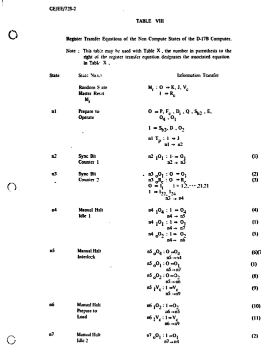
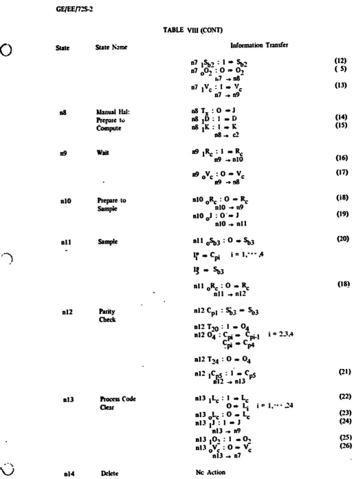
State Des-c•ription of the D-17B
Operation of the D17-h may be described by considering the various confi.urations that the
control flip-flops enter when the machine is executing a program. Thus, a state of the machine is
defined by a particular .:onfiguration of the control flip-flops. States may be represented on a
diagram which depicts the various paths that the machine many cycle through during program execution. This
state diagram may be used in conjunction with a description of the information exchange between
registers to completely describe the machine operation. The procedure used to formulate this
descrip-tion was essentially to reverse the process of computer design as described by Cho (Ref 10). Any
number of different state descriptions may result, depending upon the set of two state elements
(flip-flops) that are chosen as control elements of the machine. The control elements used in this
particular description were picked b) trial and er.or using the following criteria:
1) The states of tive machine should be closely parallel to the existing descriptions of the
GElEE172S.2
'F 14 123 f" 121 122 'w 1 "9 '1% 'I 114 113 19 P - 'ti lq T'Y 4 15 1~13 "A
1
2 11 t1
Sea 9"A" an 'I ha.,aON
Ip 124 '" T2 T 120 VW 10 12 116 TO T14~ 133; 1 12 Th TIC OTOT 71615V&13 12 I to 1 X
Pig. Compute U0172 Witd Forma (Fro Re :1 7
GE/EE/72S.2
"2)
The overall state description should be as simple as possible, yet there should be a sufficientC•
number of states to describe all the machine operations.State Descriptions have the advantage of being a visual descript.on, hence, they are easily
under-stood and awe capable of displaying large amounts of information in a concise form. Even more
"mn-portant, the state diagram provides a systematic approach for describing how the computer functions.
Register Transfer Noa:mon. In order to conveniently describe information transfer between
registers during each state it is neces-ary to adopt a type of shorthant convention to condense the
description. The symbols used in this notation are listed in Table ViI and a-e an adaptation of the
system used by Chu (Ref 10:378).
State DiaRam. In this report the siates of the computer have been broken into two major
classes or modes, Compute (K) and Non.Compute (K'). This division was selected to allow the reader
to easily correlate the state description with deseriptions already published. The states in these classes
ate represented by nodes (circles) and ate numbered with an identifying number. Configurations of
the major control flip-flops which cause transition between states are !Wsed. beside the transition path
on the diagram. Associated with each state diagrAtu is a table whkib lists the states by ,umber and
name and the information transfer which occurs during that state. The Non-Computc states arc
dis-plaged in Figs. 8 and 9 and Table VIII lists the associated register transfer notation. Compute states
. are shown in Fig. 10. 11, 12, and Table LX lists the register transfer notation. Table X is a list of
boolean equations associated with the register transfer statements in Tables Vili and IX.
,ssumption. F3r the purpose of this description, it is assumed that there is a control panel
associated with the computer which supplies the input signals listed in Table V (Ref 8 and Ref 13).
These inputs are changed to the voltage level required for use inside the computer. After this voltage
transfomnation is completed. the signal is renamed and given a * designation. The "starred" signals
are in a direct logical relationship with their generating signal: for example, when T€ is a logical "I."
T is also a logical "I"
Non Compute States. (Ref 11:56 and 15:1.1-2.15)
Power on Random State. When power is applied to the D-17B, the controlling flip-flops will
become activated in a random stale. Depressing the .MASTER RESET" switch causes the computer
to enter a Prepare to Operate state where initilization is begun (See Fig. 8).
Prepare to Operate (nl). In this state the phase register is inithlited to an idkl mode. Fc is
turned off to prevent the computer from entering , special state called fine countdown. The Discrete
GEIEE/72S-2
TABLE VII
Register Transfer Notation Used in the State Description of the D-17B Computer
Symbol Description of Symbol
( ) Parentheses denc-te contents of a register.
[ 1 Square brackets d.note a portion of a register.
.o[ A lower case o in licates the operand address
part of the instrumtion.
41 I A loweer case c inlicates the channel c' dic operand
address.
-1 ]A lower cases indicates the sector portion of the
operand address.
OP[ I Lower case op indicates operation code portion of
an instruction.
Q I Lower case f indicates the flag field of an instruction.
spI I Lower case sp indicates next k-.•uction sector portion of an instruction.
sf I Lower case sf indicates the flag storage location of
of a flag store instruction.
l[ ] Lower case I designates the left half-word of a
register:
1
] Low~er case r designates the right half-word of aregiser.
M(P) These symbols indicate a word location of memory
W cs ) designated by P or by chainel c and sector s.
W (€,s)) This symbol designates the contents of the above memory word location.
Double arrow indicates the transfer of one register (or part of a register) to another register.
+ This symbol means arithmetic addition.
This symbol means arithmetic subtraction.
x This symbol means the multiplication operation.
A colon following a Boolean statement indicates
that when the Boolean statement is true the
sub-sequent operations occur.
-. A single arrow denotes the sequence of operations
ftom one state to another.
This symbol indicates that the two state device
- ,.J(flipr-flop) )., is "one" .et. 'Zero" setting is
ex-pressed with-a preceding zero subscript.
GE/EE/72S-2"v
TABLE ViI (cont)
101
Definitiea ofSmo Symbol
a This symbol indicj1tes die excluisive or operation.
this symbol idicdates the logical and operation.
0
0
GEIEE(172S.2
V. 3 w
1-c? 0 Qý 040;
*%*'O .0t. a 2W
0402O
*af
o 44
C)
*. Fig.8 D-17B3 Notw~omputc taeGE/EE/72S-2
GEJEE/'-1S2
TABLE VIII
C)
Hegiser Transfer Equations of the Non Compute States of the D.17B Computer. Note : This tab:a may be used with Table X, the number in parenthesis to theright of the register transfer equation designates the associated equation in TabL- X.
State State Na.1! L-iformation Transfer
Random S ate Mr :O * K. J. Ve
Master Res:t 1 20 Re
Mr
DI Prepare to 0 P, Fc . Di Q Sb2 E.
Operate 04, co
I Sb3. D .0-,
nl Tp -. I ! J
nIT n2
n2 Sync sit n2. O1 : I.- 0 1 (i)
Counter 1 a2-, n3
i3 Sync Bit .n3 00,: O i (2)
Counter 2 .3 O~I. i= : 0 RW 0 (3)
"",..I,* .I1
I * 12), I.
P4 ManualHalt v4104:1 O4 (4)
Idle I n4-.a5
n4- n7
n4 002 : 1• 01
(5)
a4. ns
n5 Manual Halt n5 004 (6)X7)
Intero.-k n.a -+n4
as 501 : 0 ,-01 (I)
a.5-+ 0'
as 002 : 0 -,3, (8)
as --.nA
U6 Manual llalt F6 102 : 1 -*02 (10)
Prepare to a6 -;n5
Load n6!V€ :-*V. (II)
n6 -. n9
.7Manual Halt n7 001 :1 -01~ (2)
Idle 2 -, n4
[image:41.660.59.582.43.764.2]GE/EE/72S-2
TABLE ViII (CONT)
0
State State Name Information Transfern7 Sb2 :ISb2 (12)
0 00 : 0 - 0,)5
0? -n8
67 Ivc : I 11c
(13)
n7 09
a8 Manual b1: n8 Tx o 1 (14)
Prepare to n8 : !D (14)
Compute n8 1K: I K (15)
9-8 c2
09 Wait n9 iR: 1 Re
D9 -UnlO (16)
a, oVc : 0 - VC (17)
[
~n9
-+, 98010 Prepare to nlO oRc: 0 R (-8)
Sample 010 OJ : 0"-*,, n1O -. n9 (19)
n1O -b nil
all sample a I :0 SO (20)
[
,u
sj'..C1
o. %
i=3:
ni
R-:s.
(IS)
Snl
It oRC: 0o*
R€
1
nil ., ni2
1i2 Parity n12 CpI :S%3- SO3
Check
n12 T20 : 1 04
0h2 04." C - Ci.I i =2-44
n12 T24 : 0 04
n12 IC_5 : n'12
I!Cp
n1 h3 5 (21)n13 Process Code ni3 iLc: I LC (22)
Clear O0 Li iJ-- i"24
a13 L 0: OII 1 - .
(23)
n13 1J : I - J (24)
hi3 -. n9
n13 i02 :1 0 (25)
n13 o0 : o- vc,
(26)
[image:42.637.72.588.65.761.2]f
GE/EE/72S-2
TABLE VIDKCONT)
state State Natme Infofmution Timnsfei
RI
315Itepare to nt15003 : 0 - 03 (27)
Fail .1s 1J.I 1 j (24)
015 -~n9
315 jc, : 1 .O, (25)
0~
oC 31 : (26)
.16 ptepare to n16 103 : 1 .03 (S2)
Verify
W16 -. 19
W16 1021: 1
~02
(25)816 cy c(26)
W16 07
N? mbers n17 164 :1 a04 (28)
p 1&
0p
LCp17
i2,3n17 Lc(23)LC :0
m17 1i : I J (24)
n17.4.9
317 102 : 1 0,) (25)
u17 OV V .0 ,0 7 (26)
ni8 Location 218 lIC : c3 (53)
n1ST -
-818
if
*:1
3i(24)
.18 DIP.1
018 102) 0Vc: 1 -0 0, 0 Z-VC (25X26)
.19 Enter .19 1A I-Ac (34)
frI IFVflVerify (L) -*A
IWe .19 ,I : I -j (24)
R19 n19
81 coc:I- ,,0 V (25)(26)
019-., 0
fyi OD : 0 mD (35)
(j v2 Fdl-Vcrify fV2 1003: S * 1i,0b (36)
Scurch 2.0i
GE/EE/72S-2
TABLE VII(CONT)
0
State State Name Information Transfer(i) -* Cbi-7 i = 8,.--,12
fv2 1DIE:I1D I - E
fv2 -* fv3
fv3 Fdl-Verif (Cb) & C
Wait2 (4M(C) *N
Word times fv3oD:O fv3 *.fv4D (39)
fv4 Fill-VrCify fv4 lp: I p (41)
Execute
nz- (sill +1 -,s[1I
f,4 o1p : o I p (40)
(A) - M ( 0 [11))o
only)
fv4 oE ID :.0 -* E , I D (42X43)
fv4 fvI
fv4, Sb2 : 1 - Sb 0= V€ (44)
n19 -+ nlO
20 Mt n2o oVc : o Vc (29)
C.3. n21
n21 sun copt n321 102 AV : n21 - n4 -*1 02 ' Vc (25X30)
SCompute
.1et-n22
Program Halt n22 IDoE:I D,0 E (14X31)
fv4 ". fvi
22 1O2 004 J :1 -- 0-, (25)
n21-6 04. 04: (32)
I j (33)
n22 .ý- n7 o0 n4
---GEIEE/72S-:!
C13 C12
From Propme to Compute
c3l
cl
Sim I X-spec 0 C30
X-Srw Inst Rearcl Y-Spe-_
S-Y.Spoc
c29 0
c4O P E C38
SCL c:5 llý
Oý 0! Oi ol c2 010203 04 CII ssu
mup I-Reed 0.
da 03 0% N-Sewc 1 40j 04
0 1 CIO
041 - 0 SAO
UPY
0&
0 0
c42 0 0 P 10- 0 sunC9
SUP
I 0
40-W, 0 ce
0 So
c43 a. ADD
SUM
c7
04 CLA
TRA cs
T#Al
c3 Lan Word
Tkme Of
K
Di
n22
K Hot
U,
Fog.100.178 Cw"te SLaes
GEIEEIP2S.2
I0I
Fig i
U-pc CompueC State0
(-.e
GE/EE.172S-2
GE/EE/72S.2
TABLE IX
()
~Re;Wser
TrmAnsfr Equations for the Compute States of the D.17B Contputet. Note: Thih table may be used Aith Table X . the numberin parenti•Lis to :hl right of the r