Computationally efficient quantum-mechanical technique to calculate
the direct tunneling gate current in metal-oxide-semiconductor structures
M. M. A. Hakim and A. Haquea)
Department of Electrical and Electronic Engineering, Bangladesh University of Engineering and Technology, Dhaka 1000, Bangladesh
共Received 16 January 2003; accepted 12 May 2003兲
We propose a computationally efficient, accurate and numerically stable quantum-mechanical technique to calculate the direct tunneling共DT兲gate current in metal-oxide-semiconductor共MOS兲 structures. Knowledge of the imaginary part ⌫ of the complex eigenenergy of the quasi-bound inversion layer states is required to estimate the lifetimes of these states. Exploiting the numerically obtained exponential dependence of ⌫ on the thickness of the gate-dielectric layer even in the sub-1-nm-thickness regime, we have simplified the determination of⌫ in devices where it is too small to be calculated directly. It is also shown that the MOS electrostatics, calculated self-consistently with open boundary conditions, is independent of the dielectric layer thickness provided that the other parameters remain unchanged. Utilizing these findings, a computationally efficient and numerically stable method is developed for calculating the tunneling current–gate
voltage characteristics. The validity of the proposed model is demonstrated by comparing simulation
results with experimental data. Sample calculations for MOS transistors with high-K gate-dielectric materials are also presented. This model is particularly suitable for DT current calculation in devices with thicker gate dielectrics and in device or process characterization from the tunneling current measurement. © 2003 American Institute of Physics. 关DOI: 10.1063/1.1589173兴
I. INTRODUCTION
Current scaling of metal-oxide-semiconductor field-effect-transistors共MOSFET兲has led to the fabrication of de-vices in the sub-100-nm regime. In such dede-vices, a large gate current flows due to the direct tunneling 共DT兲of inversion carriers. This DT current is important from both device per-formance and characterization points of view. Many studies have been reported on the modeling of direct tunneling gate current.1–12 These studies can be broadly classified into a semiclassical 共SC兲2– 4and a quantum-mechanical 共QM兲1,7–9 method. SC techniques are based on the calculation of the transmission probability, usually employ the WKB approxi-mation, and often ignore the two-dimensional共2D兲nature of the inversion electrons. A modified WKB approximation has been proposed in Ref. 5 to include the effects of reflections from potential discontinuities. This approximation has been applied in Ref. 6 with reasonable success to obtain quantita-tive agreement between model and experiment. On the other hand, QM methods consider the finite lifetime of the quasi-bound, 2D inversion carriers. QM methods are preferred when Schro¨dinger’s equation is to be solved with open boundary conditions including the effects of wave function penetration into the gate dielectric. A number of recent stud-ies have compared the two DT current calculation techniques in MOS devices.8,10,11While the QM methods have a more rigorous physical basis and provide more accurate simulation results, they are also numerically more complicated to apply in practical situations. Because of the numerical difficulties,
meaningful results could hardly be obtained in Ref. 10 using a QM method for MOS structures with gate-oxide thickness greater than 3 nm, even though calculation of the tunneling current through such thick oxide layers is necessary in many applications, e.g., flash memory devices and device and pro-cess characterization from the tunneling current measure-ment. For this reason, in spite of the known accuracy of the QM methods, SC techniques are often used although many of the approximations involved in the SC techniques cannot yet be physically justified.
In this article, we propose a computationally efficient technique to calculate the DT gate current in MOSFETs us-ing a QM method. This technique is accurate and is free from the numerical limitations of the existing QM methods. The effect of wave function penetration on self-consistent elec-trostatic potential is also accounted for. This effect has re-cently been shown to be an important factor for accurate modeling of DT current.12
II. MATHEMATICAL MODEL
In our QM model, we make the approximations usually invoked in most DT current calculations.1–12 One-dimensional 共1D兲 calculation is performed to determine the self-consistent potential profile. We assume that the tunnel-ing rate is small enough so that the inversion carriers can be taken to be in thermal equilibrium. The conduction electrons are described in terms of single-band effective mass Hamil-tonian and electrons in the gate-dielectric region are repre-sented by a constant effective mass mox with a parabolic
dispersion relationship. Although a few recent studies have focused on determining mox in SiO2 and a number of other
a兲Author to whom correspondence should be addressed; electronic mail:
2046
high-K dielectric materials,13 in the absence of detailed knowledge about the bandstructures of the dielectric materi-als, moxis still widely treated as a fitting parameter.
When electrons tunnel out of a MOS inversion layer, the system becomes quasibound with finite lifetimes of the in-version carriers. In such a system, the eigenenergies are com-plex quantities: Ei j→Ei j⫹i⌫i j. Here, the real part Ei jis the energy of the jth quasi-bound state in the ith valley and the imaginary part⌫i j is related to the lifetimei j of the corre-sponding state following the relationship i j⫽ប/2⌫i j. Ac-cording to the QM methods, the DT current is calculated from the known values ofi j using Eq.共1兲:
J⫽
兺
i j
eNi j
i j
, 共1兲
where, Ni j, the concentration of the inversion electrons in the j th state of the ith valley, is given by
Ni j⫽
nvimdikT
ប2 ln
冋
1⫹exp冉
EF⫺Ei j
kT
冊册
. 共2兲In Eq. 共2兲, nvi is the valley degeneracy, mdi is the density-of-states 共DOS兲 effective mass of electrons, and EF is the Fermi energy.
Many different schemes have been proposed to calculate ⌫. In Ref. 7, Schro¨dinger’s equation has been discretized using a finite difference technique. As a consequence of us-ing open boundary conditions, the Hamiltonian matrix, de-fined over a finite region of interest, becomes non-Hermitian. Numerical determination of the complex eigenvalues of the non-Hermitian matrix provides an estimation of⌫. Reference 14 has shown that the energy derivative of the phase of the reflection coefficient 共determined using the transfer matrix formalism兲around the energies of each quasi-bound state has a Lorentzian form and its full width at half-maximum 共FWHM兲 is equal to ⌫. This method has been applied in Refs. 10 and 11 to calculate the lifetimes. However, from a numerical standpoint, direct calculation of such a derivative is difficult.11Therefore, a suggestion has been made in Ref. 11 to calculate ⌫ from the diagonal element of the transfer matrix. Since the transfer matrix method itself suffers from numerical instability, we have earlier proposed another means for calculating⌫in Ref. 15. In a truly bound system, the 1D local DOS, N1D, is given by a series of delta
func-tions at the eigenenergies. When leakage occurs, N1D
broad-ens in energy and becomes a Lorentzian function. ⌫can be estimated from the FWHM of the energy broadened N1D.
The Green’s function formalism is applied to estimate N1D.
The 1D local DOS, by definition, is related to the diagonal element of the retarded Green’s function GR:16
N1D共z;E兲⫽⫺
1
Im关GR共z,z;E兲兴, 共3兲
where z direction is normal to the silicon–dielectric inter-face. The diagonal element of GR can easily be calculated with open boundary conditions using the logarithmic deriva-tive technique, which has been described in detail in Ref. 16.
An advantage of this technique is that it is free from any matrix manipulation, and consequently, it is computationally efficient and numerically stable.
Although⌫andcan be calculated in a straightforward way using Eq.共3兲, it requires N1D to be resolved in energy
with sufficient accuracy to calculate the FWHM. Normally, in devices with gate-oxide thickness (Tox) equal to less than
2.5 nm, this poses no serious limitation. However, in struc-tures with Tox⭓3 nm, ⌫is very small and its determination
demands precisions which are much higher than usual thus requiring very high computational time. A similar situation arises in modeling MOSFETs with high-K gate-dielectric materials. As Tox goes below 1 nm, to reduce the DT gate
current and to increase reliability, the ITRS roadmap has called for possible replacement of SiO2 by high-K gate
di-electric materials.17 Due to the higher physical thickness of the high-K dielectric layers for a given equivalent oxide thickness共EOT兲, the tunneling rate decreases and⌫becomes rather small in these devices. Also in many cases, such as trend studies for a particular technology and parameter ex-traction, it is necessary to perform DT current calculations many times for the same basic structure. Due to the necessity of solving Schro¨dinger’s and Poisson’s equations iteratively with open boundary conditions each time, the problem be-comes computationally arduous and often accuracy must be compromised in order to achieve higher speed. In the follow-ing sections, we address both these issues and provide an alternate way to perform these calculations.
III. CALCULATION OF⌫
In this section, we numerically calculate the imaginary part of the complex eigenenergy, ⌫, for a number of device structures with different gate-dielectric materials, and pro-pose an empirical expression for ⌫. This expression can be used to estimate⌫efficiently in devices where it is too small to be calculated accurately by direct evaluation of the FWHM.
Numerical results are obtained by self-consistent solu-tion of coupled Schro¨dinger’s and Poisson’s equasolu-tions. Ef-fects of wave function penetration on the self-consistent po-tential profile are taken into account by solving Schro¨dinger’s equation with open boundary conditions within the self-consistent loop and by solving Poisson’s equation over the entire MOS structure.12nMOS devices are assumed to be fabricated on共100兲silicon. Values of different parameters for共100兲silicon are given in Ref. 18. As already mentioned in Sec. II, we have treated moxas a fitting param-eter with a value equal to 0.5m0for SiO2as well as for other dielectrics. This value for SiO2 has been obtained by fitting simulated DT current with experimental data.19A metal gate with a work function equal to 4.1 eV is considered. The conduction band offsets of various dielectrics with silicon, ⌬EC, and the dielectric constants, K, of these materials are taken from Ref. 20 and are presented in Table I.
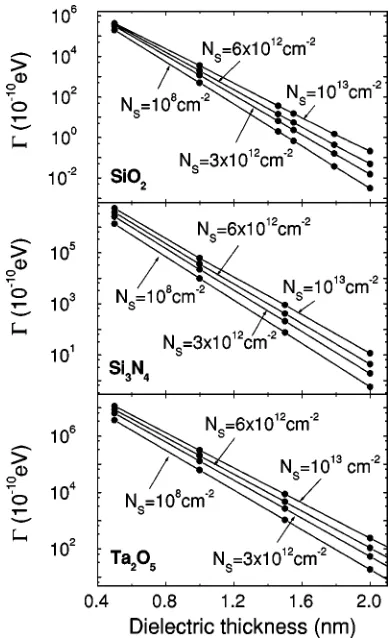
Figure 1 shows calculated⌫of the lowest energy state as a function of the physical layer thickness for three gate-dielectric materials. Substrate doping density NA
den-sity, Ns⫽兺i jNi j. It is observed that for a given Ns, ⌫ de-creases exponentially with increase in dielectric layer thick-ness for all the materials. At higher thickthick-ness of the dielectric layers, the exponential dependence is expected to hold, but it is found to be valid even for a dielectric layer thickness of 0.5 nm, where ⌫ is within two orders of magnitude of the real part of the complex energy. In practical devices, there is usually some residual oxide between the high-K dielectric and the silicon substrate. This is due to the presence of native oxide formed during fabrication. Also in some cases, SiO2-high-K dielectric stacks are fabricated intentionally to
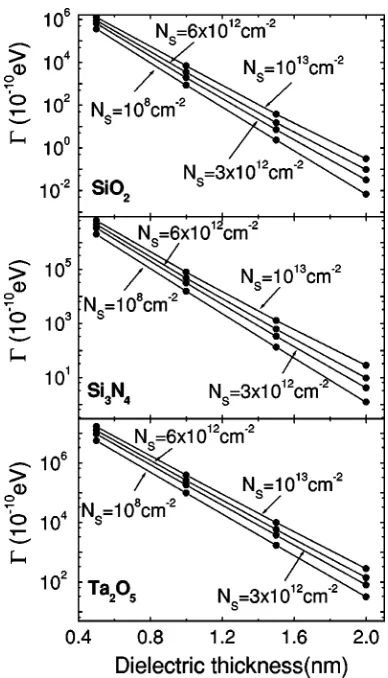
achieve a better control over the interface state density and barrier properties.20 Therefore, we investigate ⌫ for the stack-gate structures. Figure 2 shows⌫of the lowest energy state for two stack-gate structures as a function of EOT for different values of Ns. The stacks consist of a 0.5 nm native oxide layer between high-K material and silicon substrate. The value of moxand NA are the same as those used in Fig.
1. We see from Fig. 2 that ⌫ of the stack structures also depend on EOT in an exponential manner. We have also calculated⌫for higher energy states共results not shown兲and its dependence on dielectric layer thickness or EOT has been found to be similar to that of the lowest state. From these results, we propose the following empirical expression for ⌫ as a function of dielectric layer thickness:
⌫⫽⌫Oe⫺Tox/L, 共4兲
where⌫O and L are empirical constants. Toxin Eq.共4兲
rep-resents physical thickness in the case of pure dielectric lay-ers, and EOT in dielectric stacks. It should be noted that Eq. 共4兲remains valid as long as⌫for each state is much smaller than the separation between the energies of the adjacent quasi-bound states.
⌫for the lowest energy state is plotted as a function of the thickness of the dielectric layer for three different dielec-tric materials in Fig. 3 for NA⫽2⫻1018cm⫺3. Other
param-eters are the same as those used in Fig. 1. Electron effective mass mox in the gate-dielectric region also has an important effect on ⌫. mox in general, decreases with decreasing ⌬EC.13 Figure 4 is the plot of ⌫for Si3N4 and Ta2O5 gate dielectrics where mox values of 0.4 and 0.25m0 have been
used for Si3N4 and Ta2O5, respectively. From the results
presented in Figs. 1– 4, it is evident that Eq. 共4兲 remains valid for a wide range of parameter values and⌫Oand L are functions of the dielectric material, substrate doping density
NA, inversion carrier density Ns, and electron effective mass in dielectric region mox. Table II summarizes the
[image:3.612.342.534.48.337.2]ex-tracted values of⌫Oand L 共physical thickness兲as functions TABLE I. Dielectric constants and conduction band offsets at silicon–
dielectric interface for different dielectric materials used in our calculation 共see Ref. 20兲.
Material Dielectric constant, K ⌬ECto silicon共eV兲
SiO2 3.9 3.2
Si3N4 7 2
[image:3.612.51.299.85.141.2]Ta2O5 26 1.3
FIG. 1. Imaginary part of the lowest eigenenergy,⌫, as a function of physi-cal thickness of various gate dielectric layers at different inversion charge densities, NS. Substrate doping density NA⫽1018cm⫺3.
FIG. 2. ⌫, as a function of equivalent oxide thickness共EOT兲for stack gate structures at different inversion charge densities, NS. Substrate doping
[image:3.612.76.272.403.722.2]of MOS physical parameters. It is shown that L depends very weakly on Ns and NA, but is sensitive to changes in⌬EC. ⌫O increases with increasing NA and Ns and also increases with decreasing⌬EC. A reduction in mox causes ⌫O to
de-crease slightly with a corresponding inde-crease in L.
Equation共4兲can be used in a useful way to estimate⌫in devices with thicker dielectrics or with different dielectric layer thicknesses. For a given gate-dielectric material, NA and mox, we calculate ⌫ for each Ns corresponding to two small values of EOT by direct evaluation of the FWHM. Since⌫is relatively large for these devices, determination of the FWHM faces no numerical difficulty. These results are used to obtain⌫O and L for each Ns. Equation共4兲is then applied to find⌫for different values of EOT without having to perform any additional calculation. Equation 共4兲is appli-cable even where direct estimation of the FWHM is beyond the precision limit of the compiler. In order to investigate the regime of validity of Eq.共4兲,⌫has also been calculated with an energy or gate bias dependent mox. As long as moxdoes not depend on Tox, the form of Eq.共4兲is found to remain valid. It should also be pointed out that although we have reached Eq. 共4兲 using the Green’s function formalism, this relationship is quite general and is independent of the tech-nique employed to calculate⌫. Therefore, any of the existing methods7,11,14,15may be used along with Eq.共4兲to estimate⌫ efficiently in devices where it is too small to be determined directly.
IV. DT GATE CURRENT
In order to calculate the DT current, in addition to⌫, it is necessary to estimate Ni j 关Eq.共2兲兴. Ni j, in turn, depends on
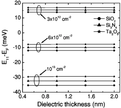
Ei j measured relative to the Fermi energy. Ei j is usually determined from the self-consistent solution of Schro¨dinger’s and Poisson’s equations. Figure 5 shows the real part of the lowest eigenenergy E11for three different dielectric materials
as a function of the dielectric layer thickness for a given substrate doping density. While for the same Ns, E11 varies
from dielectric to dielectric due to different amount of wave function penetration into the gate-dielectric region, for a given Ns and a given dielectric material, E11 is independent of the layer thickness even down to 0.5 nm. Ei j is known to be independent of dielectric material and Tox when Schro¨d-inger’s equation is solved with closed boundary conditions,18 but even the use of open boundary conditions does not make
Ei j depend on Tox for the range considered here. The same
trend is also observed for higher subbands 共results not shown兲. This implies that Ni j remains unaffected as the di-electric layer thickness is changed keeping other parameters the same. Consequently, to calculate the DT current in de-vices with different dielectric layer thicknesses, Ni j obtained for a device with a thinner dielectric layer during estimation of⌫Oand L may be used instead of resolving Schro¨dinger’s equation each time. To calculate the gate voltage correspond-ing to a certain inversion carrier density Ns, one typically uses Eq. 共5兲:
[image:4.612.343.535.48.342.2]VGS⫽Vox⫹s⫹ms⫹Vpoly. 共5兲
FIG. 3. ⌫vs physical thickness of various gate dielectric layers at different
[image:4.612.77.271.49.388.2]NSfor a substrate doping density NA⫽2⫻1018cm⫺3.
Here, Voxis the voltage drop across the dielectric layer,sis the silicon surface potential,ms is the work function differ-ence, and Vpolyis the voltage drop due to depletion effects in
the polysilicon gate. We have verified that even in strong inversion, the relationship Vox⫽ToxFox can be used to
esti-mate the voltage drop across the dielectric layer with an error less than 1%. Here, Foxis the electric field within the
dielec-tric at the silicon–dielecdielec-tric interface. In Fig. 6, silicon sur-face potential s for different dielectrics are presented as a function of the dielectric layer thickness. Again we find that
s is different for different dielectrics due to wave function penetration effects 共the differences increasing with increas-ing Ns), but for a given dielectric material and a given Ns,
s does not depend on the thickness of the dielectric layer for a thickness as low as 0.5 nm. We have also observed that
Vpolyis independent of the thickness of the dielectric layer. From the above discussion, it is evident that the need for solving Schro¨dinger’s and Poisson’s equations self-consistently each time is completely eliminated in calculat-ing the DT current through dielectric layers of different thicknesses. Once MOS electrostatics is self-consistently solved for two structures with thinner gate dielectric layers,
the obtained information can be used in a computationally efficient and straightforward way to accurately determine the DT current and the corresponding gate voltage in similar structures at any other dielectric layer thickness. Thus the problem of calculating the tunneling current–gate voltage
characteristics is greatly simplified for cases where it is
nec-essary to perform the calculation in a device with a thick dielectric layer or in similar structures with many different dielectric layer thicknesses. Such situations may arise in flash memory devices and in device and process character-ization by tunneling current measurement.
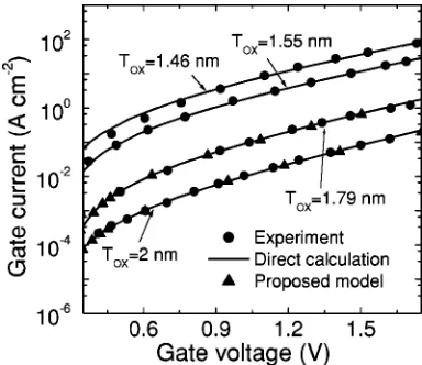
[image:5.612.127.486.65.235.2]We now check the validity of the proposed model by comparing our simulated DT current with experimental data. For this purpose, we consider MOS devices with SiO2 gate dielectric. The substrate and the polysilicon doping densities are 5⫻1017and 1020cm⫺3, respectively. Figure 7 is the plot of our simulated DT current evaluated using two different techniques. Both techniques use Eq. 共1兲 for the current cal-culation. In the first method, ⌫i j for all four devices is ob-tained by direct evaluation of the FWHM of the energy broadened 1D DOS and MOS electrostatics is independently calculated each time. In the second method,⌫i j for the two devices with Tox⫽1.46 and 1.55 nm are estimated by direct TABLE II. Extracted values of⌫Oand L关Eq.共4兲兴for different combinations of MOS physical parameters.
Physical parameters
Dielectric materials and mox
SiO2
(mox⫽0.5m0)
Si3N4
(mox⫽0.5m0)
Si3N4
(mox⫽0.4m0) NA
(cm⫺3)
Ns
(cm⫺2) ⌫ O 共meV兲
L 共nm兲
⌫O 共meV兲
L 共nm兲
⌫O 共meV兲
L 共nm兲
1018 108 10.5 0.082 18.3 0.102 16.2 0.114
3⫻1012 16.3 0.086 30.0 0.105 26.9 0.118
6⫻1012 19.4 0.089 37.9 0.108 34.2 0.121
1013 22.2 0.094 47.0 0.112 42.9 0.125
2⫻1018 108 15.3 0.083 25.5 0.103 22.7 0.115
3⫻1012 22.0 0.086 37.3 0.107 33.5 0.119
6⫻1012 25.9 0.088 44.4 0.110 40.2 0.123
1013 30.1 0.091 52.5 0.114 48.2 0.127
[image:5.612.76.271.549.723.2]FIG. 5. Real part of the lowest eigenenergy, measured relative to the Fermi energy, as a function of the physical thickness of various gate dielectric layers.
FIG. 6. Silicon surface potentialsas a function of the physical thickness
[image:5.612.341.534.561.731.2]calculation of the FWHM. These values are used to obtain ⌫Oand L at each Ns. Equation共4兲then gives⌫i jrequired to calculate the DT gate current in the two devices with thicker gate-oxide layers. Ni j,s, Vpoly, and Foxfor the two thicker devices are also obtained from the corresponding values in the thinner devices. Results of the two simulation techniques are found to be identical. Excellent agreement between simu-lation and measurement共data taken from Ref. 6兲is achieved which demonstrates the accuracy of the proposed method.
Next, the proposed technique is applied to calculate DT gate current in MOS structures with high-K gate dielectrics where direct evaluation of⌫requires extremely high numeri-cal precision. Device parameters are as mentioned in Sect. III. Figure 8 shows DT gate current as a function of gate voltage for Si3N4and Ta2O5gate-dielectric materials at three
values of EOT. As expected, for a given EOT, the current decreases significantly with increase in dielectric constant. This is due to the fact that the physical thickness of the dielectric layer increases with an increase in the dielectric constant when EOT remains fixed. Higher slope of the gate current for Ta2O5 dielectric has been attributed to its lower
value of ⌬EC, in agreement with the results of Ref. 7. In
Fig. 8, we have calculated gate current as low as 10⫺45A cm⫺2without running into any numerical difficulty. Such low current would have been extremely difficult to cal-culate using the existing QM techniques.
Finally, we study the gate current through dielectric stacks in Fig. 9. The stack structures are described in Sec. III. Again, using the proposed technique, we have been able to estimate very low values of the gate current without any computational difficulty. It is observed that the gate current increases sharply when a pure high-K dielectric layer is re-placed by a stack structure with the same EOT. The reason for this increase is the reduction in the physical thickness of the dielectric layer as pointed out in Ref. 7. This phenom-enon is particularly stronger in devices with higher EOT and lower ⌬EC.
V. CONCLUSIONS
We have proposed a computationally efficient, accurate, and numerically stable QM technique for calculating the di-rect tunneling gate current in MOS devices. Utilizing the numerically obtained exponential dependence of the inverse lifetime of the quasi-bound states on dielectric layer thick-ness, we have suggested an easy way for estimating lifetimes in devices with thicker gate dielectrics where direct determi-nation is very difficult due to numerical limitations. When DT current in many similar devices with different dielectric layer thicknesses is to be calculated, independence of the MOS electrostatics on the thickness of the dielectric layer eliminates the need for self-consistent solutions of Schro¨d-inger’s and Poisson’s equations in all structures except for two with thinner dielectric layers. As a consequence, calcu-lation of the tunneling current is greatly simplified. The va-lidity of our method has been demonstrated by comparing simulated results with experimental data. Sample calcula-tions of the DT gate current in MOSFETs with high-K gate dielectric have been presented which shows the effectiveness of the proposed technique.
1
[image:6.612.343.532.50.215.2]S. H. Lo, D. A. Buchanan, Y. Taur, and W. Wang, IEEE Electron Device Lett. 18, 209共1997兲.
FIG. 7. Comparison of the simulated DT gate current, calculated by two different approaches, with experimental result from共Ref. 6兲Here SiO2is the
[image:6.612.78.270.51.217.2]gate-dielectric material.
FIG. 8. Simulated DT gate current in MOSFETs with pure high-K gate-dielectric materials for different values of EOT. Calculations are performed using the proposed technique.
[image:6.612.78.268.558.722.2]2A. Schenk and G. Heiser, J. Appl. Phys. 81, 7900共1997兲. 3
E. M. Vogel, K. Z. Ahmed, B. Hornung, W. K. Henson, P. K. McLarty, G. Lucovsky, J. R. Hauser, and J. J. Wortman, IEEE Trans. Electron Devices 45, 1350共1998兲.
4H. Y. Yang, H. Niimi, and G. Lucovsky, J. Appl. Phys. 83, 2327共1998兲. 5
L. F. Register, E. Rosenbaum, and K. Yang, Appl. Phys. Lett. 74, 457 共1999兲.
6N. Yang, W. K. Henson, J. R. Hauser, and J. J. Wortman, IEEE Trans.
Electron Devices 46, 1464共1999兲.
7S. Mudanai, Y.-Y. Fan, Q. Ouyang, A. F. Tasch, and S. K. Banerjee, IEEE
Trans. Electron Devices 47, 1851共2000兲.
8E. Cassan, P. Dollfus, S. Galdin, and P. Hesto, IEEE Trans. Electron
De-vices 48, 715共2001兲.
9K. Alam, S. Zaman, M. M. Chowdhury, M. R. Khan, and A. Haque, J.
Appl. Phys. 92, 937共2002兲.
10
A. D. Serra, A. Abramo, P. Palestri, L. Selmi, and F. Widdershoven, IEEE Trans. Electron Devices 48, 1811共2001兲.
11R. Clerc, A. Spinelli, G. Ghibaudo, and G. Pananakakis, J. Appl. Phys. 91,
1400共2002兲.
12M. M. A. Hakim and A. Haque, IEEE Trans. Electron Devices 49, 1669 共2002兲.
13Y.-C. Yeo, T.-J. King, and C. Hu, Appl. Phys. Lett. 81, 2091共2002兲. 14
G. Gildenblat, B. Gelmont, and S. Vatannia, J. Appl. Phys. 77, 6327 共1995兲.
15A. Rahman and A. Haque, Solid-State Electron. 45, 755共2001兲. 16A. Haque and A. N. Khondker, J. Appl. Phys. 84, 5802共1998兲. 17The International Technology Roadmap for Semiconductors共ITRS兲;
avail-able on-line athttp://public.itrs.net/Files/2001ITRS/home.htm
18F. Stern, Phys. Rev. B 5, 4891共1972兲. 19
A. Ghetti, C.-T. Liu, M. Mastrapasqua, and E. Sangiorgi, Solid-State Elec-tron. 44, 1523共2000兲.
20