Cost-Performance Analysis of Printed Circuit
Boards Using Hybrid Stackup
Javid Aliyev
Telecommunication Engineering University of Twente Enschede, the Netherlands [email protected]
Wouter Stapper
Sintecs BV Hengelo, the Netherlands [email protected]Frank Leferink
Telecommunication EngineeringUniversity of Twente Enschede, the Netherlands
Abstract—FR-4 sheets are widely used among electrical engi-neers and designers as a printed circuit board base material. However, as the data rates keep on growing, signals propagating in this media get significantly attenuated. For these designs, high-frequency laminates tend to be a more common, but costly, choice. This paper focuses on full channel signal integrity analysis of the hybrid stackup, as a way of reducing the cost. Simulations on the proposed hybrid stackup, both in frequency and time domain, illustrate a significant improvement over a standard FR-4 structure. Moreover, the results obtained from the measurements show a coherency with the simulation results, thus, proving the concept. This research gives designers the ability to control the performance on desired layers, yet still, reduce the cost with standard FR-4 on the remaining portion of the board.
Index Terms—High-speed signaling, hybrid stackup, signal integrity, EMC, cost-performance analysis.
I. INTRODUCTION
Digital circuits continue to conquer higher speeds, with components such as microprocessors and signal converters routinely performing billions of operations per second [1]. The trend of modern electronic systems is leaning toward smaller form factor, complex functionalities, and higher speed with high reliability. Signal integrity (SI) becomes an issue and challenge in designing high-speed interconnects on PCB. Along with the rapid growth of signal speed and wiring density, many other factors, such as impedance discontinuities in transmission lines and poor plated-through-hole (PTH) interconnections between layers on multilayer circuit boards affect SI. As the transfer rate of the link increases, attenu-ation and dispersion of a signal propagating through a PCB transmission line become more significant. Several works have been devoted to the study of equalization [2], re-drivers [3], re-timers or low loss materials [4] to improve the performance. Other works investigated the optimization of vias [5] and differential transmission lines [6], the effect of stubs, stitching vias and type of anti-pads [7]. However, not much research has been done on the influence of this optimization on the overall cost. Cost control must be considered in the early phases of the PCB design process and in some cases even in the actual circuit development. All additional process steps have an associated cost in terms of process times, materials, consumables, energy and waste treatment.
Often designers make a mistake by choosing the expensive low loss material, while simple FR-4 would be good enough for the required performance. Therefore, it is becoming more important to use a less-costly combination of materials to achieve a good compromise between cost and performance. Studies of hybrid PCB stackup have been conducted in [8] and [9]. In this paper, the investigation focuses on a more detailed full channel signal integrity analysis based on the proposed hybrid stackup, where only specific layers of the PCB use low loss dielectric while the others are fabricated with traditional FR-4. The performance of FR-4, hybrid and low loss stackups has been compared using Hyperlynx from Mentor Graphics. Moreover, measurements in both, frequency and time domain, have been conducted. The aim of the research is to show that the board designers can get a better opportunity of using cheaper material by doing the cost-performance optimization to meet design goals without sacrificing performance.
The remaining of this paper is organized as follows. Section II introduces different PCB routing configurations considered in this work; Section III discusses the results of the simulations on HyperLynx. The test board design along with the practical measurements for both domains are reported in Section IV, whereas Sections V gives the conclusions of the paper.
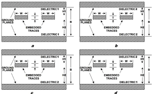
II. PCB ROUTINGCONFIGURATIONS
trace and the close by return plane will be higher. The optimal performance can be achieved by using the low loss at thinner layer (Figure 1d), as most of the energy of the transmitting signals will be in the thinner layer [11].
Fig. 1. PCB routing configurations considered in this work. Dielectric 1 represents conventional FR-4. Dielectric 2 corresponds to low loss material.
It is widely documented [12] that differential signaling gives advantages in terms of noise immunity. PCB designers use differential pair routing for high-speed interconnection for better signal integrity performance compared to the single-ended. If properly designed, reduced electromagnetic interfer-ence (EMI) due to the cancellation of the magnetic fields can be observed. From a signal integrity standpoint, differential signaling is more robust, in that it is less susceptible to external common mode noise. Therefore, in this paper, data signals are transmitted using differential signaling.
As the dielectric surrounding the central conductor of a stripline is homogeneous, varying the distance between the central conductor of the stripline and the reference plane gives different coupling strength to the ground. Some interesting effect can arise when considering a stripline merged in an inhomogeneous dielectric. In order to build a multi-layer board many dielectric and copper foils must be pressed one onto the other, and not all the foils have the same characteristics. It can happen that striplines are merged into a prepreg and a core layer, which means that the resin content in the dielectrics is different and consequently also the dielectric constant is different [13]. As a result, it is possible to have a common mode to differential mode conversion along the line [14]. When the dielectric 1 differs from dielectric 2 on both thickness and dielectric constant (r), then crosstalk
also becomes a factor that has to be considered. Under this circumstance, the propagation velocity at the top side of the routing differs from that in the bottom side of the transmission line, which causes the far-end crosstalk (FEXT) levels to increase. Therefore, selecting materials for stripline to have same or similar r helps in controlling crosstalk.
[image:2.612.49.300.107.262.2]The structure of some boards has been analyzed and finally a reference board to study has been chosen. As it can be seen (Figure 2) there are six metal layers, and two layers dedicated to high-speed digital lines (INT1 and INT2). This reference
Fig. 2. Reference board stackup used for simulations.
board has a stackup that is suitable for testing two stripline configurations with different dielectric materials. Figure 2 represents a stackup with FR-4 on top and hybrid on the bottom (Figure 1 a, d), while for the simulations, materials can be changed to test all four stripline configurations.
III. SIMULATIONRESULTS
The overall loss of transmission lines with high/low loss dielectric materials depends on material selection, stackup, and so forth. Simulations can be used to estimate the PCB trace behavior. All the configurations shown in Figure 1 have been modeled using HyperLynx 3D Explorer and HyperL-ynx SI PI Thermal. Using HyperLHyperL-ynx, hardware engineers can easily perform protocol-specific compliance checks. This simulation technology for high-performance designs provides S-parameters in the frequency domain and eye diagrams in the time domain for specific transmission lines while allowing pre-layout optimization. In the following sections, the results are presented.
A. Frequency domain simulations
These simulations have been performed and simulated creat-ing the model (Figure 2) with HyperLynx 3D Explorer, which allows having precise results. All the transmission lines are targeted to 100Ωdifferential. Trace separation is kept at 254
µm. The trace width values are 85, 90 and 95 µm, for FR-4, hybrid and low loss configurations, respectively. This way the impedance is matched and the impact on insertion loss (IL) is mainly due to dielectric properties. For differential stripline with asymmetric structure, details about the design formulas can be found in [15]. The FR-4 material has a relative permittivity (r) equal to 4.1 and a loss tangent equal to 0.025.
For low loss material,r is 3.8 and the loss tangent is 0.009.
The metal has conductivity equal to 5.8E7 S/m. S-parameters for 10 cm long traces are extracted.
Fig. 3. Insertion Loss for four cases of Fig. 1.
[image:3.612.319.558.463.668.2]simulated S-parameter of four stripline configurations (Figure 1). The differential IL, SDD21, in the frequency domain, has information about the nature of the losses. As expected, IL curves of hybrid transmission lines are bounded by those corresponding to homogeneous routing. Loss improvement can easily be seen in this graph. FR-4 based stripline has an IL equal to -7 dB at 12 GHz, while for hybrid (Fig. 1d) the IL is -4.9 dB. The resulting improvement is about 2.1 dB for 10 cm transmission line, and the gain can be even more significant with the increase of frequency/length or use of the low loss material with better loss tangent. Moreover, for lower frequencies the IL is monotonic, suggesting the drop is dominated by conductor and dielectric losses. The variations in SDD21 for higher frequencies (e.g. in case of FR-4 stripline) suggest the possible presence of impedance discontinuities.
Fig. 4. Far-end crosstalk for four cases of Fig. 1.
While in symmetric or homogeneous cases the crosstalk curves stay at a very low value at all frequencies on the
range up to 20 GHz, for the modeled pairs at given pair to pair spacing, a hybrid stripline having thickness ratio as 1:2 and dielectric layers of differentr can induce a significantly
higher crosstalk level. Figure 4 provides a far-end crosstalk (FEXT) profile for four structures. It is evident that the low loss material structure (Fig. 1b) has the smallest loss, under the same routing length, as shown in Figure 3. However, the signal’s amplitude is larger when the loss is decreased. The crosstalk index also increases correspondingly. Therefore, as can be seen from Figure 4, the FEXT of low loss structure is higher than the FEXT of the FR-4 structure. For very short routing, with similar signal amplitude, the opposite effect is observed. On the other hand, with the employment of the hybrid stackup, the FEXT goes up from -49.6 dB to -34.78 dB at 12 GHz. This impact on FEXT needs to be considered in the selection of a PCB stackup. Crosstalk increase can be controlled either by increasing pair to pair spacing or selecting materials of similar property in forming the hybrid, FR-4 or all low loss PCB stack-up. Due to the property of stripline, increasing pair to pair spacing reduces crosstalk very efficiently.
B. Time domain simulations
In this section, the improvement on SI performance in the time domain when using hybrid stackup on high-speed sig-naling is investigated. These simulations have been performed using HyperLynx SI PI Thermal linking together all the S-parameter blocks composing each structure (differential traces, vias). SerDes wizard compliance mode is used, which does not require external models as the transmitters and receiver devices are modelled using behavioral reference models based on the requirements of the specific standard used for simulations [16]. PCIe 3.0-8Gts protocol is simulated by sweeping the length of the traces from 10 to 40 cm with 302 steps.
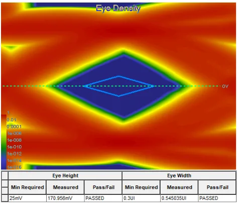
Fig. 5. Eye diagram of a hybrid stackup for 20 cm trace.
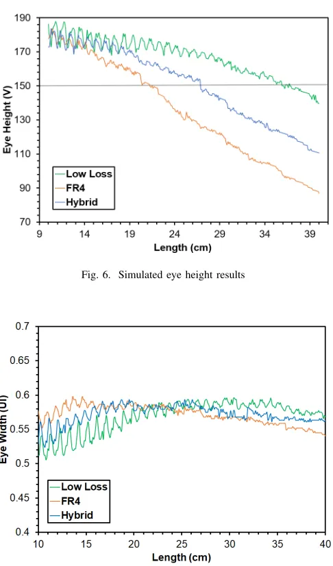
[image:3.612.54.295.473.672.2]The eye diagram gives us two main performance metrics: the eye height (EH) and the eye width (EW). The EH difference results from noises, while the EW difference results from the time jitter of the signal. The simulated EH under different routing length is shown in Figure 6. There is a noticeable improvement in the performance of the hybrid stackup over FR-4. On the other hand, for EW, the three structures exhibit similar behavior with curves fluctuating between 0.51 and 0.59 UI (Figure 7). This behavior is due to its sensitivity to reflections, as one would observe noticeable dips in return loss periodic with frequency in the response.
Fig. 6. Simulated eye height results
Fig. 7. Simulated eye width results
If 0.15 V is taken as the threshold, the estimated routing length for FR-4, hybrid and low loss structures are close to 21.5 cm, 26.9 cm and 36 cm, respectively. Therefore, an increase of about 5.4 cm on the maximum routing length can be supported by switching from FR-4 to the hybrid structure. This is an important finding in the understanding of the cost-performance analysis.
IV. EXPERIMENTS WITH PCB TRANSMISSION LINES
In this section, the results obtained from the measurements are reported, starting from the introduction of the test board design to the measurement procedures, which are divided into two parts: frequency and time domain analysis. Each part needs a different instrumentation setup that is also included in the following sections.
A. Test board design
[image:4.612.54.297.199.376.2]A test board is fabricated to prove the concept and measure the loss from the board for comparison. Manufacturing capa-bility and the stackup implementation recipe for a hybrid PCB can differ among PCB manufacturers. Figure 8 illustrates the stackup provided by Exception PCB. It is a six layer stackup with asymmetric hybrid and FR-4 configurations on layer 2 and 5, respectively. Two different board materials used in the stackup are EM-827B (FR-4) and FR408HR (low loss). Table I contains the material properties of the dielectric constant as well as the loss tangent (DF). Another important observation is that the dimensions of the layers are not precisely matched. This is due to the specific layer thickness that different materials come with.
Fig. 8. Test board.
As aforementioned, high-speed boards have multiple layers, requiring many vias to route the signal from one layer to another. Figure 8 shows the vias available for production, given the manufacturing capabilities. For laser drilled µvias, the minimum drill radius is set to 0.15 mm, while for plated through-hole vias the minimum drill size is 0.2 mm. Based on research done in [17] and [18], stitching-differential via spacing lower than 1 mm is taken to give a low impedance path for the return current close enough to the signal vias. SMA End Launch connectors are used to take the measurements.
B. Frequency domain measurements
[image:4.612.321.556.339.533.2]TABLE I MATERIAL PROPERTIES.
Material Frequency Relative Permitivity
(r)
Loss Tangent (DF)
EM-827B 1 GHz 3.7 0.019
FR408HR 1 GHz 3.3 0.0096
analyzer produced by Rohde & Schwarz (ZVB 20). This instrument is able to measure in a spectrum of frequencies between 10 MHz and 20 GHz. As suggested in [19] for high frequency measurements a good calibration kit is needed in order to remove the contribution of the cables from the measurements. The Keysight 85052B 3.5 mm calibration kit is used to calibrate VNA up to 20 GHz.
Considering the possible via transitions and the locations of the high-speed digital traces, the following set of measure-ments are conducted:
1) PTH vias are used to route the signal from Layer 1 (Layer 6) to Layer 5 (Layer 2). Another pair of PTH vias is used to route the signal back to output on Top (Bottom).
2) µvias are used to route the signal from Layer 1 (Layer 6) to Layer 2 (Layer 5). Another pair ofµvias is used to route the signal back to output on Top (Bottom). 3) Combination of µvias and buried vias is used to route
the signal from Layer 1 (Layer 6) to Layer 5 (Layer 2). Another pair ofµvias and buried vias is used to route signal back to output on Top (Bottom) layer.
[image:5.612.314.560.168.364.2]Each test structure presents advantages and disadvantages. While the first case uses only a single via, it introduces a small stub. The third one does not have any stub, but it is introducing two discontinuities due to aµvia and a buried via. The following measurements are considered for three different trace length: 6 cm, 20 cm and 30 cm.
Fig. 9. Return loss of the thru built with two connectors.
While testing the board, a problem has arisen around 10 GHz. In order to investigate this behavior a structure has
been built using two connectors to form a thru to verify any possible mismatch in the connectors. Figure 9 shows a peak in the return loss around 10 GHz in the form of a wideband mismatch. This analysis concludes that there might be mismatch problems for frequencies above 10 GHz concerning the edge mount SMA connectors. Despite a range of 0-18 GHz, due to the non-optimal connector response, for the following measurements, the frequency range is reduced and considered valid up to 10 GHz.
Fig. 10. Insertion loss of 20 cm traces for different via types.
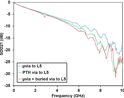
[image:5.612.49.296.476.665.2]Figure 10 illustrates the performances of different vias for specific trace length of 20 cm routed through layer 5 (FR-4 stripline). As it can be noted, in terms of insertion loss,µvias give better results, while PTH vias and a combination ofµvias and buried vias show higher loss with bigger fluctuations. The results for 6 and 30 cm traces are in accordance with the findings reported above.
Fig. 11. Insertion loss of 20 cm traces for hybrid and FR-4 structures.
[image:5.612.316.559.489.668.2]and PTH vias. As it can be observed, there is a significant difference in the high-frequency attenuation. At 8 GHz, differ-ential insertion loss are -12.71 dB (-10.63 dB) and -18.33 dB (-11.67 dB) with PTH via (µvia) transitions for the hybrid and the FR-4 structures, respectively. The resulting improvement is about 5.62 dB (1.04 dB) for 20 cm transmission line. The results obtained from the simulations are coherent with the measurements in the sense that the performance of the hybrid structure shows noticeably less loss than the FR-4 structure.
C. Time domain measurements
The second part of the measurement session involves time domain analysis, in particular using the Rohde & Schwarz SMP02 Microwave Signal Generator, MP1763C Pulse Pattern Generator and 86100A Infiniium DCA Wide-Bandwidth Os-cilloscope. The signal generator can generate PRBS with data rate up to 20 Gbps, while the oscilloscope is used to validate the operation of the serial links in the device.
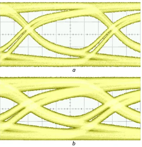
[image:6.612.57.295.424.669.2]The same set of measurements, as in the frequency domain, have been conducted. Due to the aforementioned behavior of the connectors, the measurements are considered valid up to 10 GHz. For a frequency of 6 GHz, the difference in results for 6 cm traces is insignificant. Both hybrid and FR-4, structures give similar outcomes with all three via types. With an increase in trace length, the difference becomes more significant. Figure 12 is giving an example of the performances in terms of eye diagrams of the hybrid and the FR-4 structures with 20 cm traces routed through theµvias with a frequency of 6 GHz. A significant increase in noise and jitter can be seen in the FR-4 structure, as the eye height and width differences are 22 mV and 0.04 UI, respectively.
Fig. 12. Eye diagram of a) hybrid and b) FR-4 structures for 20 cm trace.
Table II reports the parameters of the eye diagrams for each structure, via type and trace length for 6 GHz. For every via
TABLE II EYE DIAGRAM PARAMETERS
Structure Via
Configuration
Trace Length(cm)
Eye Height(mV)
Eye Width(UI)
Hybrid µvia 6 283 0.905
Hybrid µvia 20 140 0.785
Hybrid µvia 30 51 0.61
Hybrid PTH via 6 277 0.905
Hybrid PTH via 20 124 0.76
Hybrid PTH via 30 56 0.62
Hybrid µvia +
buried via 6 294 0.88
Hybrid µvia +
buried via 20 130 0.75
Hybrid µvia +
buried via 30 55 0.6
FR-4 µvia 6 274 0.9
FR-4 µvia 20 118 0.745
FR-4 µvia 30 35 0.54
FR-4 PTH via 6 274 0.915
FR-4 PTH via 20 108 0.745
FR-4 PTH via 30 35 0.55
FR-4 µvia +
buried via 6 291 0.895
FR-4 µvia +
buried via 20 118 0.73
FR-4 µvia +
buried via 30 34 0.525
type and trace length, the hybrid structure outperforms the FR-4 structure. It might also be interesting to notice that the results do not show an improved performance based on the type of via used for routing.
V. CONCLUSION
In this paper, a hybrid stackup is proposed to meet high-speed channel loss requirements while maintaining low cost. According to the modeling and full-link analysis in frequency and time domains, the proposed hybrid PCB shows noticeable improvement compared to a standard FR-4 structure. This allows a longer routing length for the same voltage threshold or better insertion loss for the same trace length. A stackup test board is fabricated for loss comparison and measurements are performed using VNA in the frequency and oscilloscope with a signal generator in the time domains, which show results coherent with the simulation results. Therefore, the present findings may be considered a promising aspect for the efficient reduction of the PCB cost. One drawback of the hybrid stackup is the increased crosstalk level, which is concluded to be effectively reduced by increasing pair to pair spacing of differential traces.
VI. ACKNOWLEDGMENT
This research was supported by Sintecs BV and the Uni-versity of Twente. We are thankful to our colleagues, Tom Berends, Henk Mengerink, Hans Klos, Maarten Tettero, Kris Boxem, Evert Pap, Fleur Oude Alink, Fidan Mammadli, Lilian Hannink, Hendrikus de Vries, who provided expertise that greatly assisted the research.
REFERENCES
[1] Selecting PCB Materials For High-Speed Digital Circuits, Microwave Journal, 02-Aug-2017. [Online]. Available: http://www.microwavejournal.com/blogs/1-rog-blog/post/23743-selecting-pcb-materials-for-high-speed-digital-circuits. [Accessed: 28-Jul-2018].
[2] Telang, V. (2012). Equalization for High-Speed Serdes: System-level Comparison of Analog and Digital Techniques.
[3] C. Ye, X. Ye, Y. Ren, K. Xiao, O. Argueta, and N. Peterson, A new de-sign flow to evaluate high-speed SerDes link performance with re-driver, 2013 IEEE International Symposium on Electromagnetic Compatibility, pp. 575580, 2013.
[4] JENG-I, C., SANNY, H. and ELREN, Z. (2007). Characterization of Low Loss Materials for High Frequency PCB Application. ITEQ Corporation.
[5] Yao, W., Lim, J., Zhang, J., Tseng, K., Qiu, K. and Brooks, R. (2015). Design of Package BGA Pin-out for >25Gb/s High Speed SerDes Considering PCB Via Crosstalk. Cisco Systems, Inc.
[6] K. Armstrong, PCB design techniques for the SI and EMC of Gb/s dif-ferential transmission lines, 2006 17th International Zurich Symposium on Electromagnetic Compatibility, pp. 359362, 2006.
[7] [6]A. Ippich, ”Influence of Via Stub Length and Antipad Size on the Insertion Loss Profile”, IPC APEX EXPO Conference Proceedings, 2014.
[8] T. Su, J. Hsu, C. Ye, X. Ye, and A. Grigoras, Signaling enabler in high-speed system design by using hybrid stackup printed circuit board, 2013 8th International Microsystems, Packaging, Assembly and Circuits Technology Conference (IMPACT), pp. 8588, 2013.
[9] C. M. Ruiz, C. Ye, X. Ye, E. Lopez, M. Yin, J. Hsu, and T. Su, Improve signal integrity performance by using hybrid PCB stackup, 2013 IEEE International Symposium on Electromagnetic Compatibility, pp. 317321, 2013.
[10] Intel.com. (2014). Hybrid PCB Stack-up. Optimization of PCB Cost and Loss Performance. [online] Available at: https://www.intel.com/content/dam/www/public/us/en/documents /design-guides/hybrid-pcb-stack-up-guide.pdf [Accessed 28 Jul. 2018]. [11] S. C. Thierauf, High-speed circuit board signal integrity. Artech House
Publishers, 2017
[12] S. H. Hall and H. L. Heck, Advanced signal integrity for high-speed digital designs. Oxford: Wiley-Blackwell, 2009.
[13] A. Figura, Characterization and Optimization of High-Speed Serial Communication Channels, pp. 191, Apr. 2014.
[14] A. Jaze, B. Archambeault, and S. Connor, Differential mode to common mode conversion on differential signal vias due to asymmetric GND via configurations, 2013 IEEE International Symposium on Electromagnetic Compatibility, pp. 735740, 2013.
[15] Wadell, Brian C., Transmission Line Design Handbook, Artech House, Norwood, MA, 1991
[16] C. Filip, SerDes Design Part 1: Take the First Steps Towards SerDes Channel Compliance, Robin Bornoffs blog RSS. [Online]. Available: https://blogs.mentor.com/hyperblog/blog/2018/02/22/serdes-design-part-1-take-the-first-steps-towards-serdes-channel-compliance/. [Accessed: 02-Aug-2018].
[17] G. Blando, J.R. Miller, I. Novak, Losses Induced by Asymmetry in Differential Transmission Lines, Manuscript for DesignCon 2007, Santa Clara, CA.
[18] Altera Corporation, Via Optimization Techniques for High-Speed Chan-nel Designs, Application Note 529, AN-529-1.0, May 2008
[19] Agilent Technologies, Stripline TRL Calibration Fixture for 10-Gigabit Interconnection Analysis, Application note, 5989-4897EN, USA April 2006
[20] Pap, E., & Krikke, R. (2015). D5.1 Hardware requirements of all bricks and tray (a). Disaggregated Recursive Datacentre-in-a-Box,687632nd ser., 1-44. Retrieved August/September, 2018.
[21] Mehta, N. (n.d.). Xilinx 7 Series FPGAs: User Guide Lite. Retrieved September 12, 2018, from
https://www.embedded.com/design/programmable-logic/4215274/Xilinx-7-Series-FPGAs–User-Guide-Lite
[22] 7 Series FPGAs Data Sheet: Overview (DS180) -Xilinx. (n.d.). Retrieved August/September, 2018, from https://www.xilinx.com/support/documentation/data sheets
/ds180 7Series Overview.pdf
[23] A. Schweitzer, Cost Drivers in Manufacturing of PCBs, in Fineline Excelence in PCB, 11-Jan-2017.
[24] A. Wright, ”Controlling PCB Costs: Part 1”, Blog.epectec.com, 2018. [Online]. Available: https://blog.epectec.com/controlling-pcb-costs-part-1. [Accessed: 02- Jul- 2018].
[25] J. Coonrod, Designing with high frequency materials: understanding the primary and secondary performance requirements in a high frequency application can help designers determine the most suitable materials to use., Printed Circuit Design & Fab, pp. 2630, 01-Mar-2009.
[26] Song, E., Cho, J., Kim, J., Shim, Y., Kim, G. and Kim, J. (2010). Modeling and Design Optimization of a Wideband Passive Equalizer on PCB Based on Near-End Crosstalk and Reflections for High-Speed Serial Data Transmission. IEEE Transactions on Electromagnetic Com-patibility, 52(2), pp.410-420.
[27] Ki Jin Han, Hayato Takeuchi and Swaminathan, M. (2008). Eye-Pattern Design for High-Speed Differential Links Using Extended Passive Equalization. IEEE Transactions on Advanced Packaging, 31(2), pp.246-257.
[28] J. Zhang, J. Lim, W. Yao, K. Qiu, and R. Brooks, PCB via to trace return loss optimization for >25Gbps serial links, 2014 IEEE International Symposium on Electromagnetic Compatibility (EMC), pp. 619624, 2014.
[29] J. Zhang, A. C. Scogna, J. Fan, B. Archambeault, J. L. Drewniak, and A. Orlandi, A hybrid stack-up of printed circuit board for high-speed networking systems, 2012 IEEE International Symposium on Electromagnetic Compatibility, pp. 554559, 2012.
[30] E. Bogatin, Signal and Power Integrity (simplied) - Second Edition, Prentice Hall, 2012
[31] M. Swaminathan, A. Ege Engin, Power Integrity modeling and Design for Semiconductors and Systems, Prentice Hall, 2007
[32] H. Johnson, M. Graham, High-Speed Digital Design - A Handbook of Black Magic, Prentice Hall, 1993