CONTROL CABINET
A part of the electronic model for tides and storm surges
S. Ishiguro 19&0
[This document should not be cited in a published bibliography, and is supplied for the use of the recipient only].
I N S T I T U T E OF OCEAIMOGRAPHIC S C I E N C E S
% %
Wormley, Godalming, Surrey, G U 8 BUB.
(042-879-4141)
(Director: Dr. A . S. Laughton)
Bidston Observatory,
Birkenhead,
Merseyside, L43 7 R A .
(051-652-2396)
(Assistant Director: Dr. D. E. Cartwright)
Crossway,
Taunton,
Somerset, T A 1 2DW.
(0823-86211)
MARCH 1980
CONTROL CABINET
A part of tlie electronic model for tides and storm surges
S, Ishiguro 1 9 6 0
Institute of Oceanographic Sciences, Worraley, Godalraing,
Abstract 2
1. Introduction 2
2. Electronic construction 3
3. Circuit description 6
4. Power supply unit 26
5. Physical construction 32
6. Circuit connection 42
7. Conclusion 55
Acknowledgements 55
References 55
Appendix 56
30 diagrams and 31 tables
ABSTRACT
Described here is the construction of the 'Control Cabinet' which controls the electronic model for tides and storm surges and its peri-pheral instruments. The most frequently used modes of operation in the system are programmed, and can be selected by a single control. Details of some operations are determined by a few additional controls. Some circuits for peripheral instruments and the power supply unit are contained in tlie cabinet. This paper includes a complete set of tables of circuit connections, and aims to aid their maintenance.
1. INTRODUCTION
The 'Control Cabinet' is a part of the electronic model for tides and storm surges, and designed to control most parts of the model system.
Fig. 1 shows the block diagram of the control cabinet by which most of the input and output circuits in the model system, including its peripheral instruments, are combined and controlled.
The blocks are linked by data channels and control channels. The control channels carry timing signals, circuit selection signals, gain control signals and some other signals for determining details of operation. The selection of a particular mode of operation, from several programmed modes, is carried out by the central control (SW8 on the front panel of the cabinet).
There are several local controls which control details of an operation, e.g. the start of an action which is selected by the main control. These controls are either on the main control panel or on each peripheral instrument.
There are a few data-bus lines which carry 8-bit data signals. These are switched either mechanically or electronically (3-state impedance control) through the same central control.
Fig. 2 shows a diagram of main parts of the timing control circuits which is extracted from the general circuit diagram of the system.
Symbol BD indicates a block of the circuits which is assembled on a single circuit board. Although each block contains circuits other than the timing control circuits, these are omitted from this figure.
Numbers on the edge of each block in the figure indicate connector pin numbers which are commonly used throughout this paper.
The timing control circuits are used to keep the best data processing efficiency in an operation mode which involves peripheral instruments (or circuits) having different speed limits. The timing control circuits are especially effective when the timing of input data signal is not regular. The principle of the circuit is to allow the access of each word of input data only after the execution of the previous word, by the output instru-ment, has been confirmed through its feed-back circuit. The circuit shown in Fig. 2 has been designed so that an appropriate combination of blocks and a feed-back circuit can be obtained automatically, when BDll is con-trolled through SW8 by which data flows are also" simultaneously concon-trolled.
(KGT)
TAPE READER
MET INPUT DATA PROC SYSTEM
INPUT MEMORY
PROG TAPE INPUT
MAIN COMPUTATION CIRCUIT
GRID SELECTION
DATA SELECTION
SCALE SELECTION
POLE SELECTION
CLOCK
INTERNAL
EXTERNAL
TAPE PUNCH
SPEED START SYNCHRO
NUMERICAL PRINTER
NUMERICAL-MAP PRINTER
XY PLOTTER
VECTOR PLOTTER
CRO MONITOR
'CONTROL CABINET'
Fig. 1 Block diagram of the 'Control Cabinet'.
TAPE SPEED CONTROL
BD30 & 3
•LTSSS
I
3
FLAG 20-28 D SEL
P CLT
CAM 1 IT
29.
D SEL
P CLT
CAM 1 3
D SEL
P CLT
CAM 1 D SEL
P CLT
CAM 1
DELAY 4 CAM 2
-TL CAM 2
NUMERIC PRINTER
54 - ]
24 "<
23
12,
To
SC
AC
AO
CN2
XY PLOTTER
4
15 5
PUNCH COM'D
C N 2 P
CN2'
Fig. Timing control circuits.
Although the main aim of the Control Cabinet is to control the whole model system, some peripheral circuits are contained in the cabinet, in order to simplify the wiring. Therefore, the circuits involved in the control are listed here, with indications of their references. Circuits which have already been described elsewhere are omitted from this paper.
Circuit block Block No. Description
Main computation circuit - Ref. 3
Input Memory — Ref. 2
Keyboard internal circuit
BD13 A C D
This paper
Keyboard interface circuit for DEC-BCD-BIN BD3 This paper
Keyboard interface circuit for arbitrary codes BD5 This paper
Output memory
(A part of the output data processing system) BD22 Ref. 5
Tape reader interface circuits BD30
: BD31 This paper
Tape punch internal circuit - This paper
Tape punch interface circuit BD8 This paper
Numerical printer internal circuit
-This paper Appendix 1
Numerical printer interface circuit BD9 This paper
Numerical map plotting circuit BD4 Ref. 1
Meteorological input-data processing system
BD2 BD32 BD33
Ref. 4
Grid selection circuit BDIO This paper
Switching circuit BDll This paper
Example
BD8
CN7
04
Explana tion
Block No. 8.
A board containing this block is referred to by this same symbol.
Connector No. 7.
The same symbol is applied to both a PCB edge connector, and a connector on a cable.
A plug and its socket are referred to by the same symbol,
Integrated circuit 04.
The IC type number is used for the reference number of a particular package of IC, with a simplified indication. If 7400 series, 74 is omitted; e.g. 04 means 7404.
04 1 04(1)
If there is more than one package of tlie same type of IC within a board, a serial number is added as a suffix (in a diagram) or in brackets (in a text).
8
IC Pin No. 3 etc.
— O 6 Connector Pin No. 6 (for a single-sided PCB).
C6 Connector Pin No. 6 on the component-side of a PCB.
N6
CN7/6
04(l)/2
0 0 / 1 - 1 0
Connector Pin No. 6 on the non-component side of a PCB.
Connector No. 7 Pin No. 5.
IC type 7004, Package No. 1, Pin No. 2.
IC type 7400, Pin Nos. 1 to 10.
3.1 Keyboard internal circuits, B D 1 3 A , C , D
The keyboard has a set of numerical keys (0 to 9), 'punch key (P), 'correction key' (C), numerical indicator of decimal number, and lamps for an arbitrary code indicator. Each key has a Hall effect switch.
An opto-electronic punched-tape reader (GNT Model 26), which has the maximum speed of 500 characters/sec, has been used in this system. The tape reader has a set of opto-electronic circuits and a tape control circuit which are built in its case, and operated by a 24v DC supply.
BD30 and BD31 have been designed to interface between these circuits and the rest of the system. Fig. 4 shows the circuit diagrams of BD30 and BD31, together with a simplified diagram of the above-mentioned circuit (top-left of Fig. 4). The circuit boards of BD30 and BD31 are also contained in the tape reader case.
In Fig. 4, the first 8 channels are the inverters and pulse-shapers of the data signal output from the opto-electronic circuits. The 9th channel is taken from the sensor for tape-feed holes (originally sprocket holes on the tape). This output is used for detecting the movement of the tape, and symbolised as FH. Because of the small hole
size, the bias current of this channel has to be adjusted by a lOK variable resistor.
The following 3 channels are used for controlling the movement of the tape: FWD (forward with a logic High), BWD (backward), and SOL
(clutch solenoid, activated by a logic High). The tape is stationary when FWD or BWD is low. These actions are controlled either from 'Input Memory' (Ref. 2) or the rest of the circuit in the system through BD31. This selection is carried out by switch IM-GE (Input Memory - General).
When IM-GE is set to GE, the tape direction is controlled by switch F-B (Forward-Backward). When F-B is set to F, the clutch is controlled by the output of flip-flop 00/5. The 00/6 is controlled by its two input terminals; 00/2 (L to start the tape forward) and 00/5 (L to stop the tape). The start control signal to 00/2 is fed either from CN3/3 (auto-matic) or switch START (manual), depending on the setting of switch W-R (Memory Write-Read). The stop control signal to 00/5 is fed either from CN3/9 (FH signal) or CN3/11 ('255' signal) depending on the setting of W-R.
If W-R is set to W, the tape starts (forward) only when START is activated manually, and stops only when '255' signal is fed from an
external circuit. The '255' signal is a code represented by a binary word 1111 1111. Consequently, the tape runs continuously from its start to the time when the '255' signal is fed. If W-R is set to R, the tape starts (forward) only when an external signal is fed into CN3/14, and stops only when the FH signal is activated by the next feed hole on the tape. Consequently, the tape moves in a step-by-step mode, one word per signal on CN/14.
A similar mode of operation to the previous mode, but with a step for every few words, is required for some applications. In this case, a signal for stopping the tape is fed into CN3/17, together with con-stant DC voltage for the, relay through CN3/18.
A tape punch (GNT Model 34), which has the maximum speed of 70 characters/sec, has been used in this system", with a minor modi-fication. Fig. 5 shows its circuit diagram.
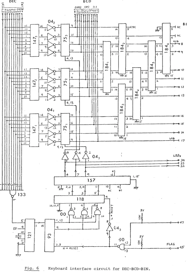
3.4 Keyboard interface circuit for DEC-BCD-BIN, BD3
BD3 has been designed to convert a 3 digit decimal number (up to 256), given on a numerical keyboard, into a binary coded decimal (BCD) number and a binary number (BIN) simultaneously. Fig. 6 shows its circuit diagram, and Fig. 14 shows the timing diagram of its essential parts. Pig. 25 shows the physical arrangement of BD3.
When a decimal number is given through the keyboard, each 147(1), 147(2) and 147(3) converts it into a BCD number simultaneously. Each of the converted BCD numbers enters into 75(1), 75(2) and 75(3) res-pectively. However, the entered code is stored in each 75 only when its control voltage (pins 4 and 13) goes into a high state. The control voltages of 75(1), 75(2) and 75(3) go high sequentially when any numerical key is activated. Consequently, the least significant BCD number is stored in 75(1), the next significant BCD number in 75(2), and the most significant number in 75(3). Then the stored 3-digit BCD number is available at the BCD output terminals.
At the same time, the BCD output is fed into a set of six 184s, so that an 8-bit binary number is available at the BIN output.
The rest of the circuit is used for generating the above-mentioned sequential control voltage for the 75s. When any key is activated, this is detected by 133, and a pulse is fed into 93 through 121. Two sets of pulses obtained from A and B of 93 are combined by 00/1-10. The combined pulses are stored in 188 (an inverted latch consists of 4 sections; 3 sections only are used), until this is reset by the
'Flag' (BD3/47) or by a correction signal ' C (BD3/45).
The output of the 118 has the required timing condition, although its polarity has to be reversed by 04(3).
157 is inserted between the 118 and 04(3) so that a similar con-version operation, but with 2-digit numbers (0 to 63), can be carried out. For a 2-digit operation, 157/1 should be kept in a high state. If this operation is not required, 157 can be omitted from BD3.
3.5 Numerical map plotting circuit, BD4
BD4 has been designed to plot a numerical map, e.g. the contours of a storm surge at a certain time. Fig. 7 shows the circuit diagram of BD4, and Fig. 8 shows its controls which are mounted on the front panel of the control cabinet. Fig. 26 shows the physical arrangement of BD4.
Since this circuit has been described in detail in a separate paper (Ref. 1), the description is omitted from this paper.
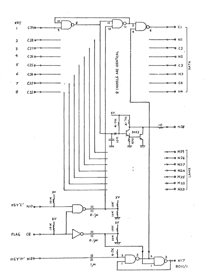
3.6 Keyboard interface circuit for arbitrary codes, BPS
BD5 has been designed to produce an arbitrary code consisting of 1 to 8 bits when the keyboard is operated appropriately. Fig. 9 shows the circuit diagram of BD5.
When any key (or keys) on the keyboard is activated, the signal is held by a flip-flop circuit connected to each key output, until the punch key (P) or the correction key CC) is activated. Each acti-vated key is indicated by a lamp on the keyboard through 3053s.
The signal from P is also held by another flip-flop circuit,
846c and B, until the 'Flag' signal from an external instrument (e.g.
a tape punch) is fed back to BD4.
3.7 Tape punch interface circuit, BD8
BDB is the interface circuit between the tape punch and other input circuits. Fig. 10 shows its circuit diagram, and Fig. 27 shows its physical arrangement.
The 8-bit input data signal is stored by 75(_1J and 75 (.2), when their control signals (Pins 4 and 131 are high, until the control signals go low. The stored data signal is fed into the tape punch data selector (a solenoid) of each 'bit channel', tkough a gate 08 and current amplifier BSY55 (operated by the +24V supply line].
A set of circuits consisting of MC19, 220nF capacitor, 220fi resistor in each output channel, and ZD33 are used for protecting the solenoid circuit from the peak voltage during the switching operation. The choice of components (including BSY55) and their values must not be modified, since they are critical in compromising the effect of protection and the maximum tape speed*.
The rest of the circuit in Fig. 10 is used for controlling the timing of operations. When START terminal (BD8/N5) is activated
(logic low), 13(2)/8 generates a pulse with a constant width. This sets two flip-flop circuits (two units of 74). ' This state is held until two external signals, CAMl (BD8/N3) and CAM2 (BD8/N4) are entered into 74/3 and 74/11 respectively. Since CAM2 is activated after CAMl, the output of 74/8 is held longer than the output of 74/6. The former controls the timing of the output current of the data signal
(8 channels simultaneously) through 00(2)/3, and also the timing of 75(1) and 75(2) through 40/8. The latter controls the timing of the tape punch clutch, by which the tape is finally punched, through 00(l)/3,
The period from the activation of START signal to the activation of CAM2 is indicated by lowering tlie 'Flag' signal (BD8/N1) which is normally high. This signal is fed back to external input circuits indicating that the given data has been punched.
SKIP signal (B D B / N2 ) is used for shifting a tape constantly without punching any data on it.
In order to control the tape punch speed, a modified signal of the 'Flag' is available at terminal BD8/C1. The pulse width of this signal is controlled by 121, so that the new data from an external input circuit cannot enter into BD8 until this signal has been completed.
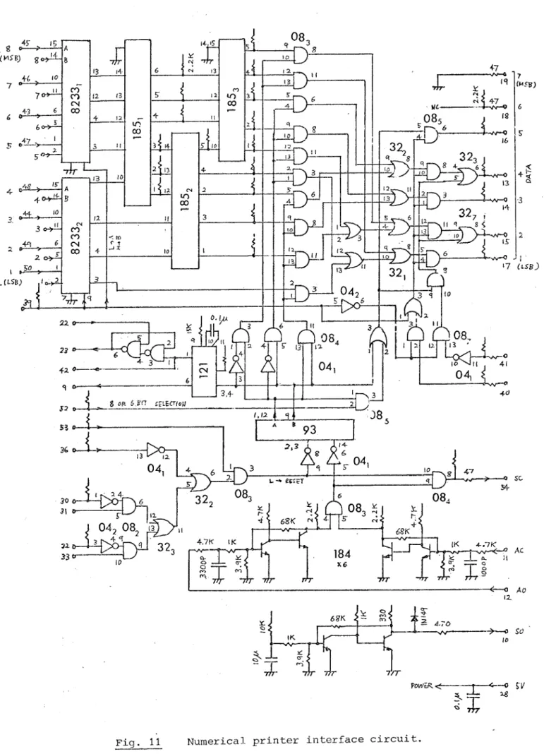
3,8 Numerical printer interface circuit, BD9
BD9 is an interface circuit between an 8-bit binary data input in the model system (e.g. the keyboard, tape reader) and the numerical printer CFACIT Model 4553) which, has an alpha-numerical character generator, driving circuit and its own interface circuit.
Fig. 11 shows the circuit diagram of BD9; Fig. 15 its timing diagram; and Fig. 28 its physical arrangement. Appendix 1 shows the block diagram of circuits contained in the numerical printer (except its character generator) and its input codes.
The top half part of Fig. 11 shows the conversion circuit for the data signal. Two sets of an 8-bit binary coded data signal are fed into 8233(1) and (2). One of them is selected by controlling their selector terminals (8233/9sl. The selected signal is converted into a 3-digit binary coded decimal number by 185(1), C2) and (3). Although the numbers of 3 digits are available simultaneously, each digit is converted into a 7-bit binary code required for the numerical printer (see Appendix II, by a specially designed conversion circuit
(the top-right part of Fig, 11) The order of the conversions of the 3 digits is controlled by 0b(4)/3, 6, 11. This circuit also generates a signal to make a space (or blank) before each set of figures.
3.9 Grid selection circuit, BDlO
BDlO has been designed to connect a set of analogue output voltages from a particular grid of the main computation network to the input terminals of the 'Output Memory' (Ref. 5). The selection of a parti-cular grid is carried out by setting a grid number on a digital numeri-cal switch (decimal 3 digit, from 000 to 999). The circuit has been designed so that the input terminals are automatically connected to this number. Fig. 12 shows the circuit diagram, and Fig. 29 shows its physical arrangement.
The output of the digital numerical switch (each digit has 10 out-put wires, but only one of them is activated at a time) is fed into the input terminals (BDlO/9-16, BDlO/25-33 and BDlO/42-50; 30 terminals in all). A signal for each digit is converted into a 4-digit binary code by 147(1) to (.3). There are three identical sets of circuits for the
3-digit figure.
There is a separate set of 3-digit binary coded decimal (BCD) signal generators consisting of 90 (.1) to 90(3). These are operated by a pulse generator consisting of 13 and BC184. The output of each digit of the generator (.3 in all)_ is compared with the output of the 147s, by comparator 20 [3 units in all), The output of the three 20s is combined by 20(4), so th.at the agreement of the number on the digital switch and the number generated by the 90s is detected. When they agree, a signal is generated which causes generation of the pulses by the 90s to stop.
The output of each of 90(1), 90(2) and 90(3) is- converted into a 7-segment numericol indicator signal by 48(1), 48(2) or 48[3), and
this is used for the LED numerical indicators on the front panel.
The output of the pulse generator, 13/6, is amplified by BFY51 and 2N3055 (operated by +24V) and used to drive the multiplexer in the main computation cabinet and the solenoid of 'Programme Tape Input" (Ref. 5) .
Instead of the above-mentioned pulse generator, a numerical pulse generating switch (SWl) has been prepared, so that a step-by-step scanning in the grid selection is possible. The automatic and manual grid selections are chosen by SW2,
In order to identify the grid no. 000 (the reference for counting), the rest of the 90(1), 90(2) and 90(3) is carried out by a 'Section Selector' (Ref. 3), through 13/8.
3.10 Switching circuit, BDll
BDll is a switching circuit by which the timing signals of the tape punch and tape reader are selected, so that their speeds match the speed of an input instrument selected by the main control switch, SW8, on the front panel of the cabinet.
BD13A PHALL EFFECT SW
I
1
3
D
9 3 6
1
o o ^ o ^ o
O
8 O
'' o 0 O
6 O
P o
t IK 1
t
r S ^
) \ }
,
) a ) 1^ '
11 ,3^ H
,a
> O ^
> > I Z LAMPS (5V, 40mA) 1 2 3 4 t i •y 6 RED o - o - o o • o - o - o - o
ttV o
FWD70 BL EL A 0 1 2 3 BL EL BL £L 936S isB MSB 5V SV 5 / Bn Or 6n Be Gy w BK Bn Bk Bo <3r Be Y Bk B n Or 6n Be Sy W Bn 4 ^ &n
COMMOW Y
Or B n
COKBECTIOK
o 6n
- + ^ LED
iKIP
9— Y
CN9
_o )
J
-O 3
4 -o E -O £
- o 7 -o 8 -0 1
-o 10 -o I I -O 12 -0 41
-o 13 —o 14 —o 15 ~Q 16 - O 17
—« 15
—o |<)
~e 20 -o 2 1
- 0 2 2
- « 2 3
- 0 2 4
-o 25 -o 26
Oi-- o 2 7
—o 2S
-A 21
- « 3 P - » 3 I ~o 3 a - 0 3 3 -9 j+ —« S'O _o 42 -o 43 -0 44
-0 3E
-o 36
-o S7
© '
0
© '
0
-©.
© -
d i
©
-© *
T
d
FWD e-TAPE READER
MODEL 26c Bwo'l
SOL
OV 2 4 /
J
C JI ~ "T" n (N
7 . 6
J J
3,-9-^ I
%
CN O I\
s:/t l
- i t y
O
D > '
-CN3 -J o I
-O 2
o
o
-« 3
\ ^ „
^ JL
04,
L 5
-0 4
-» 0 5*
U l — —
-0 6
L i
1
-0 7
—•- 0 g
0 4 ,
CK too
-A-W-i ; • n r
B D 3 0 BD31
— o 9
PH A.
—«-o 10 z © -<-o 12
r
\
sv rv
i_aj 10
2^^
471
- 3 :
220/1 RFUAY
13
H D ^
-e-« 17
-e-o 18
CN
00
FH i t
»o IF
SSS i r
' C ^ —<—I
FX -o 25
7 ^ -® 13
W-i/i
1+
> o it, cEE "iT
-<—o 14 START
:i 100
0 0
t.io - j T ion -i—SJ 1 I •jcf'
8
7
6
S
4 3 i
I
O-<S/ w
Qy Bn Y W
Bn fin VV 6n Be
INTERNAL CONNECTOR
0 e - —4 r i — ^
Or
0—rg\— 0 — — 0—rqx—
c —
0 —
0 — «—npL_
0
V
Be
Y
Bg
g
/4 15 t-6 O-17 O
Y fin
W
Bn
jul-J
t
BACK SPACE
CLUTCH
IS
19
Bn VV Y <5-n
Bo
5fCIP
f-^JC H- Be
W
Bn CARD
posnioH
10 11 12 13
Bm
)
M/ p
0 c ... ^
CAM 1
a . Be cY
:
^
Be -0V CAM 2
m g
MOTOR
KLIXOM
ll&°0 ±I0°«!
DEC
BO-CO
BCD
(100) <10} (I)
(y- o—
— rsH^fiArtcSrSNH'^ Q999Q909Q OQ <
M$5
>-t) 8
FLA 6
B I N
II
iu3
1
M-CN cn
(X
H-* RESET
TTr
Fig. 6 Keyboard interface circuit for DEC-BCD-BIN.
I 1 (LSB) 1 2 3 4-5-6 7 8 (Mis;
9 ; ^ ^ $ 9 "
CWI33 CM 13+
. &2f
ISV loK +ISI/
DG200 5 mA MAX
LED
in/75-0 (4.7V)
4 . I I
lW7fD
o
120 LBp
^ 39
t _ A J V i 2
PART OF BDq
Fig. 7 Numerical map plotting circuit.
LED
•VS/W
9 3 ( 3 ) / I , 1 2
9 3 ( 4 ) / I , 1 2
S MSB
747/12(lOOK) I A (I)
10 o
DB200/8
, — — ^ 1
747/12
9 3 ( 3 , 4 ) / 2 , 3
Common (DIG)
14 Cr
121(3)/6
00(3)/II
1 3 ( 1 ) / 1 3
IS o
17 O
0 8 / 5
0 0 ( 2 ) / I IS
o-0 4 ( 2 ) / 1 3
iq o
0 0 ( 2 )
DG200/5
20 O
747/6(100%)
+15V 35 O
rppl"' " 1
PIN ,
VIEW
L(2)
3° .3
* .2. 3° .3 1.
(H2 fHI 4—»
6 S A (H2 fHI 4—»
3 2 1
A f U
L ( l )
3 " 1' HOLD
I : 2 ' 1
Controls for the numerical map plotting circuit. Fig. 8
trEy I
3
4
S"
e
7
8
CMo-
C22<>-
C270-
C26o-C2So—4^
C 2 f f r
-
C230—>-C22fr-^
K&Y'C'
FLA 4 C8
*—»-KEY'P'
NISO—9-sv
y
O 4
/ O — I t -0. t/l
H h
i/<
<
UJ Q
09
a
> 0 CI
• > o Ml
- > 0 C2
-0 N2
- o C3
-O N3
-o
C4--O
N4--O N %
-e -o W26 -o KI27 -O N24 -0 N25" -« M22 -» 0 MZ3 J
17 8 D ! ( / |
Fig. 9 Keyboard interface circuit for arbitrary codes.
START 5 / q_3
AW?&iT
( A M I N
q - ( 3
L >
OCAM2 CH
220 1 -J
VW-J- 1 I J
FUA6-2 V O
N2°l
CLUTCH
'U WI2
S R & THE T E X T F O B Z F 3 - Q S ,
^ncl°ls AfJO^DSS.
4.13
A ' W
614/
Fiq. 10
0/ 5'/
Tape punch interface circuit.
go»:
D
— —O J A > I
17 (LSBJ
on 6 ?n jfLEcrioy
*
08,
0 8 ^
68K M I -4-1 IS"
w
30 o—
:
4.7K IK 4-.-7K
POWfcR. <-5, X "
X
-4—0 ri/ xg
Fig. 11 Numerical printer interface circuit.
10
p V 9
%
9 4 Y 9 9 4 rt
5 % s S i t S S ;
147.
20.
683 ^ n a e
13
PC
20, 6
9 0
0 4 12
B A (
VT~ '13
— o m m I ; 147 68^ 1 XI ^
84-20. 2 13
(2
10 r ^ ( =
&
Z 13
<7 6 6 Q o 9 Y ^ 60
147
68,
84,
90,
SECT/oM . , seuEcroR - <
9-O J
2 1 <•
. _ J
1-10 8 <)-i J
<3
20, 112
%
10pf
5 1 £ • /1 4 44 A
pp< H
84,
fs — M U)
90,
Z B _ d _
12 08^
5/
90,
0 4
_ %5\
13 SWI -t—9' 21 SW2 12
%
H Al-T
H 5 ^
13
sr 24/
4
BFVSI
ifzia -H
l i l i
a
^ FP6WT L ^ 0 /
ov
& R I P J E LECTORS
TIMlWfr CONTEOL SISWALI CI6,yALS FEOM SWS
I I
0-Z «
-i
o-7
tt-4 o-
ge-II o-ir 0-5
11 o-16 tf
I3e-s-5V
5
(7
0-
M-o-L | ^
0 4
0 " , ,B
i D - T
ID
o
5 4 ,
2.2K
TAPE PUUCH DEtl^E
^ ^ i = ± D n
TAPE READER MM/E
"4-lo O
, •
in o
-Fig. 13 Switching circuit.
I
I §
9 3 / 1 4
12
1 1 8 / 1
4
6
2
g '
CM T-t 1% r-O in fL4 T-H
00/12
CO EH H O H +
Q ro
K r-O lr-O PM
0 4 / 1 0
1 5 7 / 4
7
1
2
3
3
4
1
Fig. 14 Timing diagram of the keyboard interface circuit, DEC-BCD-BIN.
03 o NO
TRIGGER
DISPLAY
RECORD
C « 9 / 8 FLAG
B D 9 / 9
W COM'D
POWER
B D 9 / 1 2
10 11
5 4
9 3 / 1 4
12
BD9/16
WORD I
r
o r> ZS6/4S
WORD 2
1
iOOjUS
lis
BLAMK USD LSD BUNK MSD LSD
Fig. 15 Timing diagram of the numerical printer interface circuit.
4. POWER SUPPLY UNIT
The power supply unit provides four different voltages:
+ 2 4 v ± 7 V (5A m a x )
+ 5V ±0.25V (5A max) +15V ±0.5V (lA max) -15V ±0.5V (lA max)
The + 2 4 V supply is used for driving motors and solenoids in the
numeri-cal printer, tape punch, tape reader and grid scanners. The +5V supply is used for digital circuits, and ±15V supplies for analogue circuits such as DACs. A - 1 2 v supply required for the numerical printer is taken from the -15V supply by using a voltage divider with a zener diode.
Fig. 16 shows the circuit diagram of the power supply unit. Fixed voltage regulators in the form of integrated circuits (all in T03 cases) are used with a few discrete components.
Fig. 17 shows the physical arrangement of the components in the power supply unit. Four separate heat sinks are used for all the vol-tage regulators and rectifiers. The power switch and fuses are mounted on a small rear panel. All the reservoir capacitors are mounted on the chassis base directly.
Fig. 18 shows the printed circuit board on which two voltage regu-lators and other discrete components are mounted. The printed circuit board is surrounded by the heat sink for the voltage regulators, 7815 and 7915.
Fig, 19 shows the load regulation characteristics of each, power supply.
Also sea Fig. 21 (page 23) for the power supply unit.
The + 2 4 V supply for the numerical printer has a switch which is
FA I
I—0O0&-MIL 4610
F A 2
<—d\o—
T2 RS 207 289
FA3
>
CN ( N
z
T3 RS 196 151
psw
FILTER
[ 240vl
6 AC 6
2 4 V 7 8 H G
7 8 H 0 5 K
RC3
k " '
J
o o .
N . -4
CO
U
FD3
-cTNjo-^ 7915
(N (N
RC4
7
v:
K
N
•|5V
220
24V - I 2 V TO N U M PRINT
Gn / Be Gn/Be
Gy /Be
W B e
FILTER
78H05K 78HG
^FA3) (FA2J 1 FA
PSW
FD4) (FD3) I (FD
2 4 0 V
c=> k=r
7815 7915
with heat sink
o
o
o i
0 2
0 3
0 4
0 5 0 6
0 7
0 8
0 9
o
o 11 o 12
o 13 o 14
o o o o
n^ * 6# (y n * ^
o o o
n
10
o
=5- \
a
o cu — ^ o
\
„ ^ 'o. 1 1
te J
f
tttfrrimtrtrnrttf., m \y
/ - x w ; i •
v- x \
-•^"' ^^^^•--rrsiisvraik.iro^ \ %
y p r c s a t . .
/
^ ••"'''r-f-'^' (§;: <c> l^j
%.Q "Mfi mrnwii^mimAwr^? n <1 9
i
o
4.5
0 5 10
LOAD CURRENT (A)
Fig. 19a Load regulation characteristic of the 5V power supply.
8
i
0 5 10
LOAD CURRENT (A)
i
> 14.5
o
0.5 1.0
LOAD CURRENT (A)
Fig. 19c Load regulation characteristic of the 15V power supply.
-15-5
1
> - 1 5 . 0
ft
- 1 4 . 5 4- u.
0.5
1.0
LOAD CURRENT (A)
5. PHYSICAL CONSTRUCTION
Fig. 20 shows the control cabinet. Fig. 21 shows the rear view of the cabinet with the cover removed. The cabinet contains a circuit board rack, control panel (front), connector panel (rear), and power
supply unit including its voltage regulators. The dimensions of the cabinet are 50 x 35 x 20 (H) cm^ , and the total weight c,f the cabinet is
18 kgs.
Fig. 22 shows the details of the control panel, and Fig. 23 shows its rear view. The circuit board rack contains 9 boards, and electri-cally connected to the front panel with 5 connectors, to the rear panel with 11 groups of conductors (11 external connectors), and to the power supply with 5 groups of conductors (see Fig. 30 on page 43) .
The whole front panel can be separated, for servicing, from tha main part of the cabinet, by disconnecting the 5 connectors. Each group of controls on the front panel can also be separated from the panel without desoldering wires.
The heat sinks of the power supply unit are arranged near the rear opening of the cabinet for cooling, the 5V-supply sink (the highest temperature) being the outermost.
Figs. 24 to 29 show the physical arrangement of components cn some circuit boards (see separate papers for diagrams of board which are not shown here). These diagrams have been prepared mainly for finding the location of a particular integrated circuit on a board. The position of Pin No. 1 of each integrated circuit is shown by a small black dot in the diagrams. The location of any other component can be traced from an integrated circuit pin number.
CIRCUIT BOARD R7>CK
VOLTAGE REGULATORS
FUSE BOARD HEAT SINK
POWER UNIT
REAR PANEL
Fig. 21 Rear view of the control cabinet with the case removed.
W
G R I D N O
) S E Q G A I N
A L
r >
W i T E INT C BIP
x n
O O O
P R I N T GRID SELECT
A D R P A S ALT PLOT E XT C M O N
TPS M
r — )
A M
O
O
O
G A I N
Fig. 22 Controls on the front panel.
CN15 CN12
SW2 SW3
SW4
GRID SELECTION UNIT
NUMERICAL MAP CONTOUR
unit
5 6 7 8
2 3 4
seq
T
CN15o
Sw4 SW3 SW2 SWl BD22
ATL PAS ADR
CN13
SW6 SW8
CN14
CO
5V O
9 O 6 O
p 3 6 9 P O
3 0
BO
o 2 5 8 5 0
o o
2 0
7 0
c 1 4 7 4 O
c O
1 O
C O M O
7 8 9 o o o
866.
o o o 6 5 4
oeooooooda
0 C P
o o o
8 6 6 ,
o o o
3 2 I
9 3 6 8 9 3 6 8 9 3 6 8
Fig. 24 Keyboard internal circuit boards.
cn
• •
CO o
CK o
• •
.
o
N
lO 00
133
0
. 184,14 7,
. 04;
184,
184.
147, '^'2
n . 184,
. 04,
w) n.
184.
. 1 4 7, 1 84,
Fig. 25 Keyboard interface circuit for DEC-BCD-BIN.
D
D
D
D
D
D
O
Fig. 26 Numerical map plotting circuit.
(
)
O
(
)
O C=3
(
)
o
o
i — i
( )
c
c
O
(
o
(
o
I
!
J
c
O
BSY55J
[ = ]
CN
I 1
o
o
ro
o
oO
) )
CO I f )
o
(V.I
1
•.
0 0
o
lO
I S .o
(n
O
o
o
%
00
CZIZ3
r — 1 e z z n
Fig. 27 Tape punch interface circuit.
0 4 . 08, 08.
08,
( = 1
D
00o
o
CO CK
D
o
=
o
Q
D
o
o
m
(sD
wnT 00 wnT 00 wnT 00 wnT 00 wnT 00 wnT 00 wnT 00 wnT 00
in
CO
lo
CO
DD
O
D
(n co
•
CO
o
00
o
CO
o
o
O
u z n
[ = ]
t = ]
] O
DD
a Q
f ]
£ = = •
I 1
CM
CO
Q ] ' ,
(n co
DD
3 I )
O
t 1
CO CO cs
CO
CO CO CN CO
Fig. 28 Numerical printer interface circuit.
o
o.
48
] [
o
CO
CN
o
o
4 8
o
00
o>
3c
o
cx
4 8
o
00
o
n
<N
o
o
CN.
• • •m z i i — 1
c?
1 = 1O
r r ~ ~ i
o
CO
D
[J
cs
o
o
Fig. 29 Grid selection circuit.
6. CIRCUIT connection
The details of the whole circuit connection (except circuits within each circuit board) are shown in a series of tables in this chapter, since the use of circuit diagrams for this type of circuit (about 1000 terminals) is not practical.
Fig. 30 shows the scheme of circuit connection in the control cabinet, and this is intended to be an index to find the connection of any wire. Throughout the tables, terminal pin numbers are indicated under a circuit board number (BD ) or connector number (CN ) , with the colour of each wire.
The following abbreviation^ are
used:-Bn Brown
R Red
Or Orange
Y Yellow
Gn Green
Be Blue
V Violet
Gy Grey
W White
Bk Black Bg Beige
No wire
Example of a multi-coloured wire:
W/R White based Red stripe
Examples of combined expressions:
lo o w 0 y 1 m 0 h, % o d h-ft o 0 5 3 m n rt-•o 3 h-3 s CD o o 3 ? o n &) b: 3 O ft ^ +5V -15V +15V cnio nunel printer
cn9 keyboard
cn8 tape reader
with memory
tape punch BDll sw
cn7
bdio grid selecting
cn6 met inp data
proc system
bd9 numel print
cn5 main comput
cabinet
BD8 tape punch
O O
ext clk ext .trg •bd5 keyboard kgt
cn4 prog tape unit
BD4 nunel map
cn3 tape reader
BD3 key dec-bcd
cn2 xy plotter
bd22 output memory
cnl numel map
bd32 met inp proc s ground
4
cnl 5 CNl 2g
A
37A
50 Qi'd
hd td o h > > >71 2
s
1
i
n o >
8
h w m
h s;
I
^ s
ffi h
SW8 Main Control Switch on the Control Panel
P B 1 2 3 4 5 6 7 8 9 10 11 12
KD.T 1
Ck
1 4 / 1
Ba
1 4 / 2
R
1 4 / 3
Or
1 4 / 4
Y
1 4/ 5
Gn
14/6
Be
1 3 / 2 3
V
1 3 / 2 4 Gy
1 3 / 3 4
Or
- 1 4 / 4 5
R/Gn
KGT 2 14/7
Bn
1 4 / 8
R
1 4 / 9
Or
14/10 Y
1 4 / 1 1
Gn
1 4 / 1 2 Be
1 4/13
V
1 4/ 1 4
Gy
1 3 / 3 5
Y
— 1 4 / 4 5
R/Gn
o r 3 14/15 Ba
14/16 R
1 4 / 1 7
Or
1 4 / 1 8
Y
1 4 / 1 9
Gn
1 4 / 2 0 Be
13/27
V
1 3 / 2 8 Gy
— — — 1 4 / 4 6
R/Be
OP 4 It n ti It It It n It
T* 13/32
V/Or
1 3 / 3 3 W/Bn
1 3 / 3 1
Gn/Bn
MID 5 1 4 / 2 1
Bn 14/22 R 14/23 Or 14/24 Y
1 4 / 2 5 Gn
14/26
Be
1 4 / 2 7
V
1 4 / 2 8
Gy
13/%6 R/Bk
14/48
Or/Bn
1 5 / 3 6 Y/E
-IT 6 1 4 / 2 9 Bn
1 4 / 3 0
R
1 4 / 3 1
Or
1 4 / 3 2
Y
14/33
Gn
1 4 / 3 4 Be
1 4 / 3 5
V
1 4 / 3 6 Gy
1 3 / 2 8
Or/Gn
1 5 / 3 6 Y/R
TP6 7 It U w It It II 14/50
Gn
14/50
Gn
- 1 5 / 3 1
Bk
13/33
W/Bn
14/37
Or/R
TP8 8 M It IF II II M 1 4 / 3 5 V
1 4 / 3 6 Gy
- 1 5 / 3 1
Bk
14/37
Or/a
» 9 tt It w It II II 1 4 / 5 0
Gn
14/50
Gn
- - —
1
MAP 10 — — • • — — — ««• 1 5 / 3 0
W
1 5 / 3 3 Bn
1 3/37
Gy/Or
— 11 — " - - - - — « • — — — —
~ 12 — - - - — — - —
-Wiper 14/37
Bn 1
1 4 / 3 8
R
1 4/39
Or
1 4 / 4 0
Y
1 4 / 4 1
Gn
1 4 /4 2 Be
1 4 / 4 3
V
1 4 / 4 4
Gy
1 4 / 5 0
Gn
1 4 / 5 0 Gn
1 4 / 5 0
Gn
1 4 / 5 0
Gn
Pin No
1 Gn Common
2 W CN15/56
5 Gy CN5/8 CN6/8 CN8/8
4 V 7 7 7
5 Be 6 6 6
6 Gn 5 5 5
7 Y 4 4 4
8 Or 5 5 5
9 R 2 2 2
10 Bn 1 1 1
11 Bn CN15/21
12 a 22
15 V/Or 25 , CN5/I6
14 y 24
15 R 12
16 Be 16
17 V 17
18 Bn 11
19 Bk 20
20 Gy 18
21 w 19
22 Y 14
25 Gy CHI4/56 BD4/41
24 Y 55 42
25 Be 54 45
26 Gn 55 44
27 Y 52 45
28 Or 51 46
29 R 50 47
50 Bn 29 48
51 Gy CN5/11
52 Be +5V
Pin Wo '
N1 ¥ CNI5/9
2 Gy CNI5/27
5 . V 25
4 Be CN14/2Q
5 Gil 19
6 Y 18
7 Or 17
8 R 16
9 Bn 15
10 CN2/1
11 R 2
12 Or 5
15 Y 4
14 Gy/R B D l l / 2
15 Be CN2/5
16 V 6
1 7 - 1 8
19 Bn CNI5/2
20 R 5
2 1 Or 4
22 Y 5
25 Gy 9
24 V 8
25 Be 7
26 Gn 6
27 W/E CNI5/I8
28 W/Be 19
29 W/Gn 20 50 Be GN5/11
51 Gn 6
52 Y 7
55 Or 9
54 R 8
35 Bn 10
) 6 Gn CNI5/26
57 Y 27
3 a Or 28
39 R 10
40 Bn EXT TRI
CI Bn CNI5/I
2 E 2
5 Or 5
4 Y 4
5 Gn 5
6 Be 6
7 V 7
8 Gy 8
9 - 1 1 Gn Common
12 Bk 45V
15 R +15Y
16 Gn Common
ED55 Vector Plotting Circuit BD2 Met Input Comput Circuit
Pin No '
1 - 2 On Common
5
-4
5 a BD2/55 Via 8G4 6—9
10 • " t e ED2/31 ( x IN)
11 Y 32 ( y IN)
12 Gn 33 (% IB)
15 Be 34 (Y IN) 1 4 - 1 5
16 Or CN2'/1 (X OUT)
17 Y 2 fY OUT) 1 8 - 2 0
2 1 T5V 22 —
23 V,' DAC REF
2 4 - 2 6 —
27 Gy/Be -15V
28 —
29 R CN2'/3 (EEN LIFT)
30 P 4 (PEN LIFT) 51
Gy/a
52 Gy/a j.l5V
Pin No
1 Gy CN6/8 (LSB)
2 V 7
3 Be 6
4 5
Ga
Y ^ DATA IN
6 Or 3
7 R 2
8 Bn 1 (MSB)
9 Bk -5V
1 0 - 1 1 •M*
1 2 - 1 4 Gn Common (ANA) 15
¥
CN6/9 fFHl1 6 - 2 1
22 Gy/Be -15V
23 Gy/R + 1 5 ?
2 4 - 2 6
27 Gy SG4 28 w SG4 29 Gy SW4 30 ¥
31 Or SG4 BD33/10
32 Y SG4 11
33 Gn. SG4 12
34 Be SG4 13
3 5 - 3 8 »
3 9 - 4 1 Gn Common (DIG)
42 rnrm
43 Gn B D I I / 3 PUN COM 44
45 Be/R GN6/13 46 P 12
47 Gr-D 11 (ISB)
48 o o
49 Bn/R 18 (MSB)
50 Bk/R OUT
51 W/R
52 Y/R 15
53 Gn/R 14
54 Or C&3/17 (SG4) 55 R BD33/5 (SG4) 56 Bk SG4
Note: 'Meteorological Input-data Processing System' consists of ED52 (contained in the 'Control Cabinet'), ED53 and ED2
(both contained in external case). These are connected
10 11 12 15 14 15 16 17
1 8 - 2 0
21 22 25 24 25 26 27 28 29 50_ JL 52 55 54 55 56-58
5 9 - 4 0 4 1 - 4 5
4 1 45 46 47 ^ 49 50 51 52 55 54 55 ^ 5 l
5 8 - 6 0
V Be Gn Y Or R Bn w gy V Be Gn Y Or r Bn Bk Un Or Y un 4.5v jjri Or/Gn w Gy V Be Gn Y Or R Bn Bk cni5/24 25 CNI4/6 5 4 5 2 1 cii9/51 50 29 28 27
26
25 24 25 22 CN9/45 42 41 Common. 019/11 BD5/N10 BD5/C8 CN9/9CN9/8 BD5/C22 7 025 6 024 5 025 4 026 5 027 2 0 2 8 1 029 GN9/id
Pin No 1-2
5 Gy/R 4-15 V
4
5 Gy/Be -15 V
6
7 i.-z vV
8 —
9 Bo BD9/1 CNI6/1 10 R 2 2
11 Or 5 5
12 Y 4 4
15 Gn 5 5
14 Be 6 6
15 V 7 7 16 Gy 8 a
17 —
18 w BD9/40
19 Bk 41
20 —
21 Bk - 5 V
22 «
25 Gn Common
24 Be C N l / 4
25 V 5
26 Gy 2 27 w 1
2 8 Bk 5
29 W/R 6
:50-60
41 Gy . BD52/25 CN14/56
42 V ' 24 55
45 Be 25 54 4.4 Gn 26 55 45 Y 27 52 46 Or 28 51 47 R 29 50
48 Bn 50 29
4 9 - 5 5 —
54 W/Or B D l l / 1 5
55 Or/R CNl/7
56 V ON6/9, CN8/9, CH5/9
57 Be BD9/42
58 Or 55
-BD5 Keyboard (KGT) ED9 Numerical Printer
Pin No
N1 R CN14/8
2 Y 10
5 Be 12
4 Gy 14
5
6 w B D 2 2 / 1 4 , B 0 9 / ) l
7 Gy/R B D l l / 2
8 - 9
10 CN9/11, BD3/45
11 m 4-5V
12 Gn Common
1 5 - 1 6
17 Gy/Ba B D l l / 1
18 R GN9/12
1 4 - 2 1 —
22 V CN9/19
2) Gy 20
24 Gn 17
25 Be 18
26 Or 15
27 Y 16
28 En 15
29 R 14
50
CI Sn CN14//
2 Or 9
3 Gn 11
4 V 15
5 - 7 •ai
8 Or/Gn 2D5/47
9 - 1 0
11 Bk t5V
12 Gn Common 1 1 - 2 1 •«>
22 Gy CN9/8 BD5/49
25 V 7 50
24 Be 6 51
25 Gn 5 52
26 Y 4 55
27 Or 5 54
28 R 2 55
29 1 56
30 —
Pin
No1 Bn BD4/9
2
R •
105
Or
114
Y
125
Gn ,
156 Be 14
7
V
158 Gy 16
9
-10 R/Be,V GNlO/22 CNlO/40
11 Y/Gn 25
12
P
2115
Y
414
Or
515
R
2l6
Gn
517
Bn
118
Be
619
Y
72 0 - 2 1
22 V/Gn CN5/19 B D l l / 4 25 Gy/Be B D l l / 1 1
2 4 - 2 5 • P
26 Gjx Common
27
2 8 -5V
29
...
50 W/Or 0^15/"^
51 Gy/R BD22/14
52 Bn CN15/55
55 Or BD4/58 2 4 - 5 5 « a
26 Bk CN15/52 5 7 - 5 8
59 W GN15/51
40 w BD4/18
41 Bk 19
42 Be 57
45 Be B D 8 / a i 4 CNI4/42
44 Ox N i l 59
45
Gy
Nlo
4446 V H15 45
47 Gn N15
41
48 Y
N12
4049
R
NIO
5850 m N9 57
51 «
52 V/Be CN15/55
55 Gy/Bk
CNI5/56
Pin No 1 2 5 4 5 9 10 11 12 15 14 15 16 17 1 8 19 2 0 21 22 25 2 4 25
26
27 2a 29 50 51 33 54 55 56 57 5a 39 4 0 _41. 42 45 44. 45 46 47 4 8 49 5 ^ 51 52 55 54 55 56 ^ 58-60 Or Y Or Gy bk Gn Gy Y Y Gn Be Or r Be v Bn R Or Y Gn Gy V Y Gn Be Or R Bn w Be v m R Or Y Gn Gy v Y Gn Be Or R di w Be v bi R Or Y Gn cni5/22 21 2N5o55/Base CN5/3 +5V Gominon cl\i12/8 7 4 5 6 52
1 i_ 3 3 54 28 29 50 31 32a u 2 / i 7
16 15 14 15 12 11 10
18
40 41 55 36 57 38 39 CHI2/26 25 22 25 24 21 20 19 27_ 47 4 8 42 45 44 45 4.6DIG SW
(1)
DIG SW
(10)
DIG SW
(100)
Pin No
1 Gy/Bk BD5/N17 2 Gy/R K7
5 Gy/Gn C H 3 / I 7 ON6/I9 4 W/Gn CN5/19 BD9/22 5 R/Gn C N I 4 / 4 5
6 R/Be 46 7 Or/Bn 4 8
8
Or/GnCN13/29
9
1 0 Y/Gn BD8/k6 1 1 Gy/Be B D 9 / 2 3 12 —
15 V/Or B D 4 / 5 4 14 Bn/Be BD8/C1 15 Or/R C H I 4 / 4 7
16
Or/Be C N I 4 / 4 9 17 Gy/Or C N I 3 / 5 718
Y/R C N I 5 / 3 7 19 »2 0 W/Be C N 3 / 1 4 21
22
Gn Common25
2 4 Bk +5V
BD8 Tape Punch Drive
P i n No N1
2 R/Bk C N 7 / l 8 , C N 9 / 3 7 3 w/Be CN7/10
4 W/Or CN7/12 5
6 Y/Gn BDll/lO 7 —
8 —
9 BD9/50 c m 4 / 3 7
10 R 4 9 38
1 1 Or 4 4 39
12 Y 4 8
40
15 Gn 47 4 1 14 Be 4 3 4 2
15 V 4 6 4 3
16 Gy 4 5 4 4 17 Bk +5Y
1 8 Gn Common
19 R -24V
20
Gn Common 2 1 Gy CN7/122
V 2 2 3 Be 3 2 4 Gn 425 Y 5
26
Or6
27 R 8
2 9 R/Be 16
i 50 —
B D l l/14
CN2' (Socket) Met Input Data P S
CM} (plug) Tape Reader Pin No
1 W BD4/27
2 Gy 26
5 ¥ 25
4 Be 24
5 Bk 28
6 W/R 29
7 O r / a 55
8. Gn Common
9 - 2 5
CM2 (Socket) XY Plotter
Pin Ho
1 En BD22/10
2 R 11
5 Or 12
4 Y 15
5 Be 15
6 V 16
7 - 1 ) —
14 Gn Common
Pin No '
1 Y X axis
2 Or Y axis
5 V Z pen lift
4 R Z pen lift
5 - 1 ) —
14 Gn Common
1 5 - 2 5
Pin No
1 Bn BD52/10 CN6/1 CN8/1
2 R 9 2 2
5 Or 8 ) )
4 Y 7 4 4
5 Gn 6 5 5
6 Be 5 6 6
7 V 4 7 7
8 Gy ? 8 8
9 V BD4/56,CN6/9, CN8/9
10 Be CN8/10 11 Gy BD52/51 12 V CN8/i2
15 Gn Common.
14 W/Be B D l l / 2 0 15 Or CNI5/I5 16 V BD52/15
17 Gy/Gn CN6/19, B D l l / 5 18 R/Bk CNI5/26
19 W/Gn B D l l / 4 , BD9/22 20^24 * *
25 5V
Pin No
1 Gn Common
2 isi CNl5/10 5 R 11 4 Or 12 5 Y 15
6 Gn 14
7 Be 15 a V 16
9 Gy 17
10 y CN5/4, 5055 COL
11 R 24V
12 Gn Common
15-25 —
ON5 (Socket) Main Gompu Cab
Pin No I
1 R 24V
2 Gn Common
5 Gy BDlO/4
4 Y CN4/iO, 5055 COL
5 —
6 Gn ED22/&51
7 Y N52
8 R N54
9 Or N55
10 Ba. N55
1 1 Be BD22/N50 1 2 - 2 1 • a
22 Gy/Be -15V
25 Common
24 Gy/E 15V
25
CN6 (Socket) Met Input Data P S
Pin No
1 Ba BD52/IO CN5/1 CN8/1
2 R 9 2 2
5 Or 8 5 5
4 Y 7 4 4
5 Gn 6 5 5
6 Be 5 6 6
7 Y 4 7 7
8 Gy 3 8 8
9 w ED4/56, CN8/9,CN5/9 10 —
11 Gy CN14/28 ISB
12 V 27
15 Be 26
14 Gn 25
15 Y 2 4
16 Or 25
17 R 22
18 Bn 21
19 Gy/Gn CN5/17, B D l l / 5 2 0 - 2 1
-Gommon
GH7 (Socket) Tape Punch CN9 (Socket) Keyboard
P i n No
1 Gy BD8/N21
2 V M22
3 Be N23
• 4 Gn N24
5 Y N25
6 Or N26
7 R # 2 7
8 Bn M28
9 R +24V
10 W/Be BD8/n3 11 Gn Common 12 W/Or BD8/F4 13 Gn Cocmon 14 —
15 R +24V
16 R/Be BII8/IT29
17 R +24V
18 R/Bk BI)8/ir2, CIT9/37
19 Gn Gomnon
2 0 - 2 5
-CU8 (Socket) Tape Reader
P i n No
1 Bn B D 3 2 / 1 0 CN3/1 C # 6 / l
2 R I 9 2 2
3 Or 8 3 3
4 y 7 4 4
5 Gn 6 5 5
6 Be 5 6 6
7 V 4 7 7
8 Gy 8 8
9 W 3 D 4 / 5 6 , C N 3 / 9 , c % 6 / 9 10 Be CN3/10
11
12 V CN3/12 13 Gn Common 1 4 - 2 5
-Pin Ho
1 Bn BD5/G29 BD3/56
2 R C28 55 3 Or 0 2 7 54
4 y 0 2 6 53
5 Gn 0 2 5 52
6 Be 0 2 4 51
7 V 0 2 3 50
8 Gy 0 2 2 49 9 w BD3/48
1 0 Bk 57
1 1 Bn B B 5 / N 1 0 , BD3/45
12 R BD5/MI8
1 3 Bn BD5/H28
14 R 1T29
1 5 Or IT26
1 6 y N27
17 Gn B 2 4
1 8 $ 6 , B 2 5
•I9 V N22
20 Gy N23 21 y
2 2 Bk B&3/3O '23 Bn 2 9
24 R
28
25 Or 2726
y26
27 Gn 2 528
Be24
29 V 2 3
30 Gy 2 2
31 w 21
32 Bn Common
3 3 R Common
34 Or cmi3/34
3 5 36
37 R / B k BD8/M2,
CB7/18
38-40
—4 1 y BD3/34
4 2 Or 3 3
4 3 Gn 32
4 4 - 4 8
—49 Bk +5V
GMIO (Socket) Numerc Printer CN12 Internal Connector
Pin No
1 m BDo/17
2 R 15
5 Or 14'
4 Y 15
5 Gn 16
6 Be 18
7 V 19
8-17 —
18-2U Gn Common
21 P BD9/12
22 R/2e 10, CNlO/40
25 Y/Gn 11
24 G n A 54
25-^5
54 Gn Common
55 R +24V VIA PSW
56 Gn Common
57 Bk
58 Gn Common
59 Be Zener D (-12Y)
40 V BD9/10, CHlO/22
41-50
-Pin No 1 Plug Socket
1 Bn BDlO/15 DIG SW(1) 1
2 R 14 2
5 Or 15 5
4 Y 10 4
5 Gn 11 5
6 Ba 12 6
7 V 9 7
8 Gy 8 8
9 ¥ 16 9 10 Bn BDlO/52 DIG SW(IO) 1
11 R 51 2
12 Or 50 5
i5 Y 27 4
14 Gn 28 5
15 Be 29 6
16 V 26 7
17 Gy 25 8
18 w 55 9
19 Bn BDlO/49 DIG SW(IOO) 1
20 R 48 2
21 Or 47 5
22 Y 44 4
25 Gn 45 5
24 Be 46 6
25 V 45 7
26 Gy 42 8
27 w 50 9
28 Bn BDlO/19 IgD(l) a
29 R 20 b
50 Or 21 c
51 Y 22 d
52 Gn 25 e
55 Be 17 f
54 ¥ 18 S
55 Bn BDlO/56 lED(lO) a
56 R 57 b
57 Or 58 0
58 Y 59 d
59 Gn 40 e
40 Be 54 f
41 V 55 S
42 Bn BDlO/55 Ifn)(lOO) a
45 R 54 b
44 Or 55 c
45 Y 56 d
46 Gn 57 e
47 Be 51 f
48 V 52 g
49